E L S E V I E R Microelectronic Engineering 48 (1999) 235-238
www.elsevier.nl/iocate/mee
Characteristics of Novel Polysilicon Oxide by Anodic Oxidation
C. F. Yeh a, J. S. Liu b, and M. C. Chiang b
aDepartment of Electronics Engineering & Institute of Electronics, National Chiao-
Tung University, 1001 Ta-Hsueh Road, Hsinchu, Taiwan, R.O.C.
~,lational Nano Device Laboratories,
1001-1 Ta-Hsueh Road, Hsinchu 30050, Taiwan, R.O.C.
Abstract
For nonvolatile memory applications, a novel oxide grown on polysilicon by anodic oxidation (anodic polyoxide) is ftrst investigated. In this work, the electrical characteristics of anodic polyoxide is discussed and compared with the conventional thermal polyoxide. The results show that the anodic polyoxide exhibits considerably excellent characteristics, i.e., low leakage current, high breakdown electric field, and high reliabilities.
1. Introduction
For nonvolatile memory applications, the scaling down of device geometry requires high quality thin polyoxide in order to keep a high gate-coupling ratio and improve the data retention characteristics. However, the polyoxide films formed by high temperature oxidation still suffer from high leakage current and low dielectric strength, compared with the oxide grown on single-crystalline silicon [1-3]. These can be attributed to the non-uniform thickness of the polyoxide film and the asperity at polysilicon/polyoxide interface, which can lead to a serious enhancement of localized electric field [4-5]. In this work, anodic oxidation of polysilicon is first proposed, and anodic polyoxide is investigated and compared with conventional polyoxide prepared by furnace.
2. Experiment
40 nm-thick oxide was prepared on P-type wafers with thermal oxidation. Then, 300-nm thick in-situ doped polysilicon layer (polyl) with sheet resistance of 35 / was prepared at 550 . Anodic polyoxide was grown in 0.01wt% citric acid solution at 35 V for 3 min. For comparison, polyoxide grown by furnace at 850 was also prepared to serve as control sample (thermal polyoxide). Subsequently, a second layer of in-situ doped polysilicon (poly2) of 300-nm thick was deposited. Some anodic polyoxide samples received a post-poly2 annealing with RTP at 700 for 30 sec in N2 ambient (i.e., post-anneal samples). After defming poly2, all samples received a 500nm- thick oxide via PECVD as a passivation oxide. Contact holes were then opened, and 500nm- thick TiN/A1/TiN/Ti electrode was deposited and patterned. As shown in Fig. 1, poly2/polyoxide/poly 1 capacitors were completed. Finally, all samples were sintered at 350 for 20 min in N2 ambient. From C-V measurement, the thickness of anodic and thermal polyoxide is 7.0 nm.
3. Results and Discussion
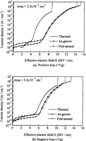
Figure 2 (a) and 2 (b) compare the current density vs electric field (J-E) characteristics under positive (+Vg) and negative (-Vg) bias for as-grown, post-annealed anodic-polyoxide samples and thermal polyoxide sample. The
236 C. Yeh et al. I Microelectronic Engineering 48 (1999) 2 3 5 - 2 3 8
Top electrode
B ~ P a s s i v a t i o n oxide
_tunnel oxide (4rim)
/
6 inch p-type wafer |
J
Fig. 1. Cross-sectional view of n+-polysilicon/
• + . .
polyoxlde/n -polyslhcon capacitors•
16 lO I 10° Area = 3.2x10"4 cm2 t w" 10" j / lO
. /
/
,,~ 10" / /= ,o
/
/
,o'
I
f
10 "6 / / '~ lO" / J ' Thermal lO • [r ~ 0 _ , . . ~ ~ • As-grown i 10 -9 ~ - ~ Post-anneal L~ lo-,O,t . . . 0 2 4 6 8 10 12 14Effective electric field E (MV / cm) (a) Positive bias (+Vg)
1 0 1 - 4 2 10 ° Area=32xlo cm ] _ ~ lO -I j J 10 .2 / f
lO-'
/ J
lO 4 / , / 7 10 4 / / / 7 101 / y , T h e r m a l 10B . ~ • As-grown 10. ~ --.~-- Post-anneal 110-0o r . . . 0 2 4 6 8 10 12 14Effective electric field E (MV / cm) (b) Negative bias (-Vg)
16
Fig. 2. J-E characteristics of anodic polyoxide compared with thermal polyoxide under (a) positive bias (+Vg) and (b) negative bias (-Vg). r..)
anodic polyoxide depicts smaller leakage current and higher onset of tunneling field than those of thermal polyoxide for both bias polarities. In addition, for anodic polyoxide the phenomenon that the onset tunneling field under bottom injection (+Vg) is lower than that under top injection (-Vg) does not appear. The higher onset of tunneling fields indicate that the enhancement of localized electric field is less severe. It implies that for anodic polyoxide the roughness at polysilicon/polyoxide interface has been reduced, compared to that of thermal polyoxide. In fact, atomic force microscopy (AFM) has verified that the roughness at polysilicon/anodic polyoxide is indeed better than that for thermal polyoxide.
Furthermore, anodic polyoxide can sustain a much higher current density near dielectric breakdown. The effective electron barrier heights under positive bias for thermal, as- grown, and post-anneal samples are 2.1, 2.7, and 2.7 ev, respectively; while those under negative bias are 2.3, 2.6, and 2.6 ev, respectively•
Figure 3 (a) and 3 (b) compare the Weibull breakdown field (Ebd) plots for as-grown, post- annealed anodic-polyoxide samples and thermal polyoxide sample under positive and negative biases, respectively• For thermal, as-grown, and post-anneal samples, the breakdown electric fields at 50% cumulative failure under positive bias are 9.1, 15.2, and 15.4 MV/cm, respectively; while under negative bias, they are 10.2, 13.9, and 14.4 MV/cm, respectively• Clearly, anodic polyoxide samples show higher breakdown field than thermal polyoxide sample under both bias polarities. This results show the anodic polyoxide has more densified film quality and more stable Si-O bond structure than thermal polyoxide.
-- 0 " 7 3 ~rea = 8x10 "5 crn 2 2 Thermal 1 = As-grown Post-anneal -2 -3 0 1
m,
~o
,L,
-2
-3
0
C. Yeh et al. / Microelectronic Engineering 48 (1999) 235-238
,+ ,+
I
//
, i . , . , . , . , . , . i " , . i . 1 2 3 4 5 6 7 8 9 10 11 12 13 14 15 16 Breakdown field (MV / cm) (a) Positive bias (+Vg)Area = 8x10 "5 cm 2
S/I
Thermal • As-grown Post-anneal ,t • ! 1 i r i . I , i . i . i . i . I . I " I " 1 2 3 4 5 6 7 8 9 10 11 12 13 14 15 16 Breakdown field (MV / cm) (b) Negative bias (-Vg)Fig. 3. W e i b u l l b r e a k d o w n field plots o f anodic p o l y o x i d e c o m p a r e d w i t h t h e r m a l p o l y o x i d e u n d e r (a) positive bias a n d (b) n e g a t i v e bias.
It is w e l l k n o w n that the h i g h e r quality oxide the less e l e c t r o n trapping. T h e W e i b u l l c h a r g e - t o - b r e a k d o w n ( Q ~ ) plots u n d e r +40 m A / c m 2 a n d -40 m A / c m 2 stress are s h o w n i n F i g u r e 4 (a) a n d 4 (b), respectively. F o r thermal, a s - g r o w n , a n d p o s t - a n n e a l samples, the Q ~ at 5 0 % c u m u l a t i v e failure u n d e r +40 m A / c m 2 stress are 0.4, 2.1, a n d 2.4 C / c m 2, respectively; w h i l e u n d e r -40 r n A / c m 2 stress, they are 0.3, 1.6, a n d 2.4 C / c m 2, respectively. A n o d i c p o l y o x i d e s a m p l e s s h o w larger Q ~ t h a n t h e r m a l p o l y o x i d e s a m p l e u n d e r b o t h c u r r e n t stresses. T h e anodic
237 p o l y o x i d e s a m p l e s i n d e e d suffer f r o m less electron t r a p p i n g a n d thus h a v e larger Q ~ t h a n t h e r m a l p o l y o x i d e sample. 2 1 - 0 -2 -3 10 "~ Area = 8x10 "5 cm 2 • J = +40mA/cm 2 , Thermal • As-grown Post-anneal ..+
/
g 10 .2 10 "1 10 ° 10 I Charge to breakdown (C / cm 2)(a) +40 mA/cm 2 stress
0 , - - 1 -2 -3 10 .3 Area = 8x10 "~ cm 2 = -40mA/cm 2 Thermal • As-grown Post-anneal
I
(
j t
S
10 .2 10 -t 10 ° 10 t Charge to breakdown (C /em 2)(b)-40 mA/cm 2 stress Fig. 4 W e i b u l l c h a r g e - t o - b r e a k d o w n plots o f a n o d i c p o l y o x i d e c o m p a r e d w i t h t h e r m a l p o l y o x i d e u n d e r (a) +40 m A / c m 2 stress a n d (b) - 40 m A / c m 2 stress. 4 . C o n c l u s i o n I n c o n c l u s i o n , a p p l i c a t i o n o f a n o d i c o x i d a t i o n
238 C. Yeh et al. / Microelectronic Engineering 48 (1999) 235-238 on polysilicon is first proposed. The anodic
polyoxide has higher effective electron barrier height, higher electric breakdown field and higher charge-to-breakdown than the conventional thermal polyoxide. A post-poly2 RTA treatment can further improve the electrical characteristics of anodic polyoxide. From these excellent characteristics, we believe that anodic polyoxide will be a highly potential candidate as high quality thin polyoxide for nonvolatile memory applications.
References
[ 1 ]
C. Cobianu, O. Popa, and D. Dascalu, "On the electrical conduction in the dielectric layers," IEEE Electron Device Lett., vol. 14, p. 213, 1993.[2] R. E. Shiner, N. R. Mielke, and R. Hag,
"Characterization and screening of SiO2 defects in EEPROM structures," Int. Reliability Phys. Syrup. IEEE Proc. pp. 248- 256, 1983.
[3] T. Ono, T. Mori, T. Ajilka, and T. Takayashiki, "Studies of thin poly-Si oxides for E and E2pROM, '' IEDM Tech. Dig., pp. 380-383, 1985.
[4] R. Anderson and D. Kerr, "Evidence for surface asperity mechanism of conductivity in oxides grown on polycrystalline silicon," J. Appl. Phys., Vol. 48, No. 11, p. 4834, Nov. 1977.
[5] H. Huff, R. Halvorson, T. Chin, and D. Guterman, "Experimental observations on conduction through polysilicon oxide," J. Electrochem. Soc., Vol. 127, No. 11, p.2482, Nov. 1980.