A 2.4-GHz Low-Flicker-Noise CMOS
Sub-Harmonic Receiver
Jin-Siang Syu, Member, IEEE, Chinchun Meng, Member, IEEE, and Chia-Ling Wang
Abstract—A 2.4-GHz low-noise sub-harmonic direct-conversion
receiver (SH-DCR) is demonstrated using standard 0.18- m CMOS technology. Deep-n-well vertical-NPN (V-NPN) bipolar junction transistors (BJTs) are employed to solve the flicker noise problem in CMOS process. Design optimization of a power-con-strained noise-impedance-matched low-noise amplifier (LNA) with the effect of lossy on-chip inductors is fully discussed in this paper. A multi-stage octet-phase polyphase filter is analyzed in detail and implemented to generate well balanced octet-phase LO signals. As a result, the demonstrated receiver achieves 51-dB voltage gain and 3-dB noise figure with flicker noise corner less than 30 kHz when GHz. The I/Q amplitude/phase mismatch is below dB/ , respectively, covering from 2.35 to 2.6 GHz. The dc current consumption is 5 mA at a 1.8-V supply.
Index Terms—Direct-conversion receiver (DCR), low-noise
am-plifier (LNA), sub-harmonic mixer (SHM), vertical-NPN (V-NPN), octet-phase.
I. INTRODUCTION
R
ECENTLY, DIRECT-CONVERSION RECEIVERs(DCRs) have been widely researched and implemented for their high integration level and low power consumption when compared with the heterodyne receivers [1]–[3]. The discrete RF image-rejection filter and the IF high-Q channel select filters of a heterodyne receiver are the two fundamental hindrances for the monolithic integration. On the contrary, the RF image-rejection filter can be eliminated in a DCR because there is no image channel. Besides, the entire CMOS DCR can be implemented alongside the baseband DSP in a single inexpensive chip. Since the DCR down-converts the RF signal directly to baseband , the power dissipation of the high-order channel-selection active filter in a DCR is lower than that in a heterodyne receiver with a higher IF frequency for the same selectivity.
However, a CMOS DCR has inherently serious flicker noise, IIP and dc offset problems because the MOS device itself has Manuscript received August 10, 2011; revised October 28, 2011; accepted March 16, 2012. Date of current version January 24, 2013. This work was sup-ported in part by the National Science Council of Taiwan under Contract NSC 99-2221-E-009-049-MY3, and Contract NSC 101-2923-E-194-003-MY3, and in part by the Ministry of Education (MoE) Aim for the Top University (ATU) Program under Contract 95W803. This paper was recommended by Associate Editor A. Tasic.
J.-S. Syu was with the Department of Electrical Engineering National Chiao Tung University, Hsinchu 30010, Taiwan. He is now with MediaTek Inc., Hsinchu 30078, Taiwan.
C. C. Meng and C.-L. Wang are with the Department of Electrical Engi-neering, National Chiao Tung University, Hsinchu 30010, Taiwan (e-mail: [email protected]).
Digital Object Identifier 10.1109/TCSI.2012.2215794
very large flicker noise and mismatch [4]. A deep-n-well ver-tical-NPN (V-NPN) bipolar junction transistor (BJT), available in a standard low-cost 0.18- m CMOS process, has low flicker noise and good device matching (beneficial for low IM and dc offset) and thus is especially suitable for a DCR [5], [6]. Further, a sub-harmonic mixer (SHM) topology is chosen in this work to achieve a low dc offset because of its additional LO rejection (LOR) [7]–[9].
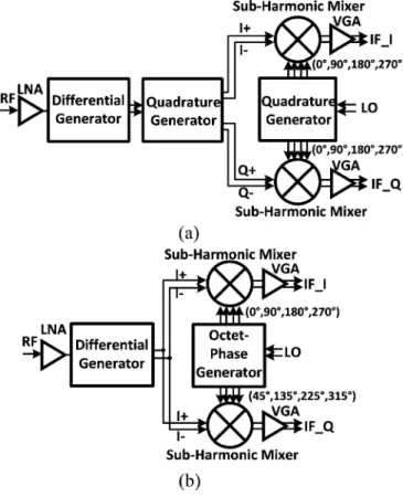
For a single-quadrature I/Q DCR, either RF or LO should be in quadrature. As a result, there are two main types of I/Q SHM topologies to achieve an I/Q SH-DCR. For the corresponding SHMs, an equivalent differential switching operation at 2LO frequency requires that the LO signal should be in quadrature as shown in Fig. 1(a) while a quadrature 2LO operation straight-forwardly requires octet-phase LO signals as shown in Fig. 1(b). Thus, Fig. 1(a) consists of both quadrature RF and LO signals [9] while Fig. 1(b) consists of differential RF but octet-phase LO signals [7], [10], [11]. The IF quadrature phase accuracy is determined by the RF quadrature generator while the quadra-ture LO signals are only used to perform a 2LO differential switching operation in the former topology. Thus, the former topology has lower loss in the LO signal generation. However, the loss of the RF quadrature generator is especially undesir-able in a high-gain low-noise receiver. On the other hand, an octet-phase LO topology can be employed to avoid the addi-tional RF loss through the gain path as long as the LO power is sufficient and balanced octet-phase LO signals can be generated. A BJT switching core requires a smaller LO power than an MOS switching core and the use of V-NPN BJT with its low cut-off frequency of 2 GHz does not cause performance degrada-tion because the LO frequency ( GHz) is only half the RF frequency for a sub-harmonic mixing operation. Thus, in this work, the latter topology incorporating a multi-stage octet-phase polyphase filter (PPF) [12] is chosen to generate well balanced octet-phase LO signals. A thorough analysis of the octet-phase polyphase filter is also described in this paper.
This paper describes the design, analysis and implementa-tion of a low-power low-noise RF receiver for 2.4-GHz-band IEEE 802.15.4 standard. Because the applications of this stan-dard are commercial, home automation, industrial, consumer electronics, personal health care, and game, these electric de-vices should operate from several months to a year on one bat-tery without changing. Thus, low cost and low power are key issues.
The block diagram of the proposed SH-DCR is shown in Fig. 1(b), including a single-ended-input LNA, I/Q SHMs with BJT switching core, I/Q variable-gain amplifiers (VGAs) and an LO octet-phase PPF. Circuit design optimizations are deeply de-scribed in Section II while Section III reports the measurement 1549-8328/$31.00 © 2012 IEEE
Fig. 1. Block diagram of an I/Q sub-harmonic direct-conversion receiver with (a) both quadrature RF and LO signals (b) differential RF and octet-phase LO signals.
results and compares with simulation results. Conclusions are given in Section IV. After detailed analysis and design optimiza-tion in each funcoptimiza-tion block, the proposed SH-DCR achieves 51-dB voltage gain and 3-dB NF at 2.4 GHz, while the total current consumption is only 5 mA. The performance is compa-rable and even better than that of other 2.4 GHz receivers based on fundamental mixing or using advanced technology.
II. CIRCUITDESIGN ANDIMPLEMENTATION
A. Low-Power LNA Design Optimization With On-Chip Low-Q Inductors at a Fixed Power Consumption
A low-noise amplifier (LNA) plays an important role in a re-ceiver and its power consumption usually dominates the whole receiver. The optimization of an LNA is urgently required. The schematic of a widely used cascode LNA with a source degen-eration inductor is shown in Fig. 2. The is used to make the optimal noise impedance and input impedance almost equal. The cascode structure provide good reverse isolation to avoid the LO leakage leaking back to the RF input and even to the an-tenna.
1) Input Matching With the Effect of Low-Q Inductors: The
input impedance of a cascode LNA, shown in Fig. 2, can be expressed as
(1)
Fig. 2. Schematic of a cascode LNA with a single-to-differential transformer connecting to the transconductance stage of the following I/Q Gilbert mixers.
where represent the series resistance of the induc-tance . Typically, is much smaller than and can
be neglected. when a parallel capacitance is
applied.
Since an on-chip planar inductor can be modeled as an in-ductor in series with a resistor when the operating fre-quency is lower than . Here, of an inductor is defined as . Generally speaking, the series resistance is propor-tional to the geometric length and thus proporpropor-tional to the series
inductance. That is, , where is close
to a constant, only relating to the geometrical shape (including metal width, spacing and metal thickness). Thus, the in (1) can be modified as
(2) To achieve impedance matching at a target resonance frequency and the target matching impedance when the device size (or ) and bias are decided,
(3) Thus
(4) and
(5) Note that, if no series resistance is considered (i.e.,
), the well-known results for impedance matching are
and .
Besides, the transconductance gain of the input transistor at resonance can be expressed as
(6)
where is
the quality factor of the input impedance.
2) PCSNIM Method With the Effect of Low-Q Inductors:
impedance matching (PCSNIM) method proposed in [13], a is applied to modify the without changing the and makes the noise and impedance matching achieved at the same time for every transistor size at a fixed when is negligible. However, when considering the extrinsic (i.e., ), the noise factor has one additional term of
when compared to the [14], i.e.,
(7) where is a constant for the channel thermal noise current, is a constant for the gate induced noise current, and is a correlation coefficient of the gate-induced noise current and the channel noise current.
Therefore, the series resistances of on-chip low-Q inductors make the NF increase dramatically and even dominate the overall NF. Instead of complicated mathematical NF deriva-tions [15], a clearer and more useful graphical method based on simulation is proposed in this paper for the NF optimization with the effect of low-Q inductors.
Here, a cascode LNA with a parallel resonance load ( at resonance) as shown in Fig. 2 is simulated for different
transistor size of , series inductance and ,
while the gate width of is 240 m and the tank is resonated at 2.4 GHz. All of the device gate lengths are kept at 0.18 m. The device model is BSIM3v3.24 provided by the foundry. Here, , and 2 /nH are simulated for both
and and the corresponding , 15, and 7.5
at 2.4 GHz. /nH is especially addressed because it is the typical value of an on-chip spiral inductor using ultra-thick metal (UTM) and metal width is 6 m while the is still higher than the operating frequency.
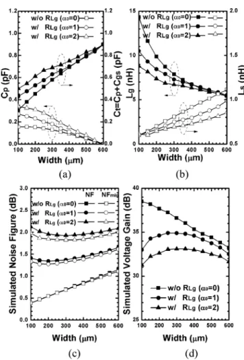
Fig. 3 shows the simulation results of the cascode LNA w/
following a PCSNIM method while mA. The
chosen for optimal noise performance and the
are drawn in Fig. 3(a). However, no is required to achieve noise matching when is larger than 600 m. The corre-sponding and are drawn in Fig. 3(b). Fig. 3(c) and (d) show the corresponding achievable NF and (voltage gain), respectively. The line with square symbols in Fig. 3(c) clearly shows the results using PCSNIM but without . When con-sidering low-Q (high- ) inductors, a higher of an inductor requires a larger to reduce the required and the corre-sponding for an optimal overall NF, as shown in Figs. 3(a) and (b). This advantage is much more significant than the reduc-tion of the device noise. As a result, when considering the , the minimum achievable NF w/ [in Fig. 3(c)] is lower than the NF w/o [in Fig. 4(b)] for a given . Note that, when
, the using PCNO decreases progressively when increases as shown in Fig. 4(c). However, when using PCSNIM with low-Q inductors, the applied degrades the overall of the LNA as shown in (6) while the device remains the same especially for a small transistor size. Thus, not only the NF but also has an optimal device size when is considered. Besides, the optimal width increases if a larger is applied as
Fig. 3. (a) and (b) and for power-constrained simultaneous noise and impedance matching at 2.4 GHz and the corresponding (c) simulated noise figure and (d) simulated voltage gain of the cascode LNA with while the supply current is 2.5 mA. The unit for is /nH.
shown in Fig. 3(c) and (d). As a result, the for minimum achievable NF is around 0.2–0.3 pF when /nH. The corresponding is around 6–7 nH, which is implementable and occupies a small die area. The minimum NF is below 2 dB and is above 33 dB when ranges from 200 to 400 m
( – A/ m).
Further, if the matching condition is not limited to a perfect 50 , i.e., a smaller matching impedance is selected, the also increases, as predicted in (6) and NF slightly decreases due to the smaller at the cost of the matching bandwidth. Thus, changing the matched impedance to around 35–40 by decreasing the results in a higher , a lower NF and allow-able matching bandwidth. Finally, the m (4- m unit width 60 fingers) is chosen to achieve both optimal NF
and .
As shown in Fig. 2, a transformer is used as the load of the cascode LNA, instead of the parallel resonance load, to transform the single-ended LNA current into differential voltage output for I/Q mixers. Thus, a 5:4 transformer is used. The line width, line spacing and the outer diameter of the implemented transformer are 9 m, 2 m and 290 m, respectively. In ad-dition, a tuning transistor is used to achieve the gain re-duction by drawing out the RF current if the gate bias of increases when a large RF signal is applied.
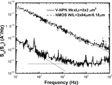
Fig. 4. Measured output noise current spectral density of the V-NPN BJT and 0.18- m NMOS device. A.
B. I/Q Sub-Harmonic Mixer Using V-NPN BJTs
The output noise current spectral density for V-NPN BJT
(with m ) and NMOS (with
m/ 0.18 m) devices is measured using an Agilent 35670A dynamic signal analyzer as shown in Fig. 4. The V-NPN BJT has roughly 400-Hz flicker noise corner at A while the NMOS device has the flicker noise corner beyond MHz at the same dc current. V-NPN BJTs can be obtained without extra cost in a deep-n-well CMOS technology [5], [6]. The source-drain diffusion functions as the emitter, the p-well as the base, and the deep-n-well as the collector.
The flicker noise of the LO switching core directly leaks to the output at the zero-crossing, while the flicker noise of the RF stage is upconverted to the odd harmonics of the LO frequency [16]. Thus, a CMOS active Gilbert mixer has a several MHz flicker noise corner and becomes an unacceptable weakness for a DCR, especially in a narrow IF band application. As a result, V-NPN BJTs are used to replace the LO core devices, directly eliminating the device flicker noise source of the LO switching core [5]. In addition, the of the V-NPN BJT are around 2 GHz, which is enough for a 2.4-GHz SHM because the LO fre-quency is only 1.2 GHz.
As shown in Fig. 5, there are three main kinds of SHMs, in-cluding stacked-LO [7], top-LO [9], [10], [17], and bottom-LO [18] topologies. A 1.8-V supply voltage, compatible to digital circuits, is not sufficient for the stacked-LO topology consisting of the cascode LO core, RF stage and IF resistive or PMOS load as shown in Fig. 5(a). Besides, if the V-NPN BJTs are applied to the LO cores in a bottom-LO SHM, as shown in Fig. 5(b), it still has severe flicker noise problem because the flicker noise of the RF transistors directly leaks to the output. However, the V-NPN BJT is not suitable for an RF stage be-cause of the low and high parasitic resistance ( , and ). On the other hand, the top-LO SHM has better 2LO-to-RF isolation than the others because the four transistors fed by the quadrature phases LO signals are connected at the emitter node, or , and thus the 2LO frequency component is inher-ently cancelled, as shown in Fig. 5(c) [19].
Fig. 5. (a) Stacked-LO sub-harmonic mixer (SHM) (b) bottom-LO SHM (c) top-LO SHM with V-NPN BJTs in LO core (d) simulated current conversion gain of the switching core for a fundamental mixer, a stacked-LO mixer and a top-LO mixer core.
As a result, the top-LO SHM as shown in Fig. 5(c) is chosen in this work to simultaneously fulfill both the supply-voltage re-quirement and the gain/noise performance. Active PMOS loads with a 2 m gate length to guarantee the flicker noise less than 10 kHz are applied in this work. The top-LO SHM requires a 3-dB larger LO power than a stacked-LO one, which is derived in Appendix B and the simulation results at GHz are drawn in Fig. 5(d) and compared to a fundamental mixer. Thus, the LO octet-phase generator should be carefully chosen and de-signed to reduce the unwanted LO loss. Although an SHM re-quires larger LO power than a fundamental mixer, there is still a flat-gain region to a certain extent and can tolerate the ampli-tude imbalance of the LO signals.
C. LO Multi-Stage Octet-Phase Polyphase Filter
A well-known multi-stage PPF is widely employed as a differential-quadrature generator [20]. However, an octet-phase PPF should be applied to generate the eight vectors required by the top-LO I/Q SHMs. As shown in Fig. 6, a single stage PPF
Fig. 6. Schematic of a multi-stage octet-phase polyphase filter.
is applied at the first stage to generate differential-quadrature
outputs (i.e., )
at the center frequency in spite of loadings [20]. The four vectors are further split into eight vectors by (8), shown at the bottom of
the page, and .
Fig. 7(a) shows the vector diagram at the second-stage output. Here, the common denominator is neglected because it only af-fects the absolute (not relative) gain and phase. Here, we define two variables to quantify the octet-phase signal accuracy
(9) and
(10)
where and .
As a result, all are the same (i.e., ) but the
PE is , which is not
acceptable in a real application.
From the third stage, the gain of each stage follows:
(11)
where and define .
Fig. 7. Phasor diagram at (a) second (b) third stage and (c) fourth stage.
Here, holds if the quadrature
signal at the first stage is perfect. The output vectors at the third stage are shown in Fig. 7(b). Thus, perfect 45 phase difference
is obtained (i.e., ) but dB.
If we extend the analysis to more stages, the results are sum-marized as follows.
1) At the even stage, the eight vectors are ,
and where is assumed. As a result, we
get (12), shown at the bottom of the page.
2) At the odd stage, the eight vectors are
, and .
Thus
(13)
Note that, following Fig. 7(a)–(c), the recursive formula can be directly obtained
(14)
and .
It is interesting that, after more stages are cascaded, perfect octet outputs with balanced amplitude/phase are achieved eventually at either the even or odd stage. The detailed deriva-tions are summarized in Appendix A. However, the voltage
(8)
Fig. 8. Die photo of the proposed 2.4-GHz sub-harmonic receiver.
loss when cascading many stages is unacceptably large. As a result, a three-stage octet-phase PPF is employed in consider-ation of both voltage loss and signal accuracy. A 0.51-dB LO amplitude imbalance is tolerable because when the LO signal is large enough for an active mixer, the mixer output amplitude imbalance is even smaller, as shown in Fig. 9(d).
Finally, an IF VGA with around 20-dB linear-in-dB tuning range is implemented using an - attenuation method [21], [22]. In addition, the V-NPN BJTs are used at the input stage because of the ultra-low flicker noise and the larger under the same dc current consumption than NMOS transistors.
III. MEASUREMENTRESULTS
The die photo of the 2.4-GHz SH-DCR is shown in Fig. 8, and the die size is 1.15 1.05 mm . On-wafer measurement facilitates the RF performance. Fig. 9 shows the conversion gain of each I/Q channel with respect to the LO power when
GHz and GHz. The CG of I/Q channel
has around 0.7-dB gain difference at low LO power. When the LO power exceeds 8 dBm, the CG of both channels is almost the same, as discussed in Section II.B. A maximum CG is 52 dB when LO power exceeds 10 dBm. However, an 8-dBm LO power is applied for all the following measurements. Note that, the simulated power loss of the LO octet-phase generator is around 8 dB.
Fig. 10(a) shows the CG and NF as a function of RF fre-quency. The peak CG is 51.2 dB at 2.35 GHz with a 1-dB band-width ranging from 2.25 to 2.45 GHz while the minimum NF is 3 dB and less than 3.5 dB within 2.3–2.55 GHz. In addition, the input return loss is better than dB from 2.0 to 2.6 GHz as shown in Fig. 10(b). Fig. 11 shows the NF with respect to IF frequency when GHz. The NF is 3 dB at the highest gain while NF is 5 or 8 dB when the LNA gain is reduced by 5 or 10 dB, respectively. Further, the NF remains around 3 dB when the IF VGA is reduced by 10 dB. The flicker corner is much less than 30 kHz, which is limited by the noise source and dc block in NF measurement.
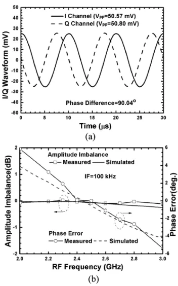
The I/Q output waveforms are shown in Fig. 12(a) with 0.04 dB gain difference and 0.04 phase error when
GHz and GHz. Fig. 12(b) shows the gain difference dB and I/Q phase error when LO frequency ranges from 2.35 to 2.6 GHz. However, the phase error increases when
Fig. 9. Conversion gain with respect to LO power of the proposed 2.4-GHz sub-harmonic receiver.
Fig. 10. (a) Conversion gain/noise figure (b) input return loss with respect to RF frequency of the proposed 2.4-GHz sub-harmonic receiver.
LO frequency is away from the designed center frequency of 1.2 GHz. Fig. 13(a) shows the CG as a function of the LNA RF tuning voltage while Fig. 13(b) indicates the CG
Fig. 11. Noise figure with respect to IF frequency of the proposed 2.4-GHz sub-harmonic receiver.
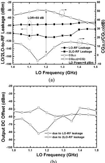
with respect to the VGA IF tuning voltage . A tuning range of around 20 dB is achieved by each RF/IF tuning scheme. Fig. 14(a) shows the and IIP at different gain condi-tions by RF gain tuning while IIP of five random chips are measured and plotted in Fig. 14(b) individually since the IIP is related to the process variations and mismatches. Thus, the mean value of the IIP is 25 dBm at highest gain with at most 2 dB variation. The LO/2LO-to-RF leakage is defined as the LO/2LO power measured at the RF input port while the re-ceiver is normally functioning with 8-dBm LO input power. Thus, the LO/2LO-to-RF leakage is less than dBm when the LO frequency ranges from 1.1 to 1.3 GHz, as shown in Fig. 15(a). The worst-case dc offset due to LO/2LO self-mixing is calculated following [11]
(14)
where represents the observed LO/2LO
leakage at the RF port and stands for the con-version gain of a mixer when input signal at LO/2LO frequency
is applied. Here, for an SH-DCR. Thus, the
dc offset due to self-mixing is strongly reduced for an SHM and 50 dB LOR at GHz is obtained, as shown in Fig. 15(a). The dc offset due to LO/2LO is drawn in Fig. 15(b). That is, an overall worst-case dc offset of 0.44 mV appears at the output. The circuit performance is summarized and compared with state-of-the-art DCRs in Table I [7], [9], [10], [23]. A MOS active mixer has typically over 1-MHz flicker noise corner [9]. Besides, even though only quadrature LO signals are required, the LO power is still high because of the MOS switching core. A separate bias of the mixer core and the RF stage is applied in [10]. PMOS devices with lower flicker noise property and a lower dc current flowing into the mixer core result in a lower flicker noise leaking to IF output [10]. On the contrary, a stage biased at a higher current can maintain sufficient linearity and noise figure of the active mixer. Passive mixer realization is an alternative for low flicker noise performance [23], [24] but the conversion loss of the passive mixer raises the NF floor if
Fig. 12. (a) I/Q waveform at GHz, GHz (b) ampli-tude imbalance and phase error of the proposed 2.4-GHz sub-harmonic receiver.
the preceding LNA does not have sufficient gain. The flicker noise problem can be avoided using SiGe HBT technology [7] or using V-NPN BJTs in low-cost CMOS process because of the device nature. However, the LO power requirement of this work is 4-dB lower than that in [7], even though the top-LO SHM in this work inherently requires 3-dB more LO power than the stacked-LO SHM in [7]. That is, the passive loss of the pro-posed octet-phase generator is very low. Table II compares the demonstrated 2.4-GHz BJT-based sub-harmonic receiver with the state-of-the-art 2.4-GHz low-power receivers based on fun-damental mixing [1]–[3], [22], [25], [26] to further manifest the excellent performance of this work.
IV. CONCLUSION
A 2.4-GHz low-noise SH-DCR is demonstrated using para-sitic V-NPN BJTs in a standard 0.18- m CMOS process. The design optimization of the LNA with the trade-offs between ex-trinsic thermal noise of low-Q inductors and intrinsic de-vice at a fixed power dissipation is fully analyzed. An octet-phase PPF is used to generate balanced octet outputs for I/Q SHMs. As a result, the maximum CG is 51 dB and minimum NF is 3 dB with the flicker noise corner less than 30 kHz when
Fig. 13. Conversion gain with respect to (a) RF tuning voltage (b) IF tuning voltage of the proposed 2.4-GHz sub-harmonic receiver.
Fig. 14. (a) and (b) of the proposed 2.4-GHz sub-harmonic receiver.
APPENDIXA
DERIVATION OFAMPLITUDE/PHASERELATIONS OF A MULTI-STAGEOCTET-PHASEPOLYPHASEFILTER For additional stages, the vector should be obtained first because both AD and PE can be formulated using it by (12) and (13). As mentioned in Section II.C,
(A1)
where .
The matrix can be eigendecomposed to where
Fig. 15. (a) LO/2LO-to-RF leakage (b) equivalent output dc offset of the pro-posed 2.4-GHz sub-harmonic receiver while the LO power is 8 dBm.
and
Thus,
(A2)
where .
When reaches infinity,
(A3) Consequently, at the stage, remains but
TABLE I
PERFORMANCECOMPARISONS OFSUB-HARMONICDIRECT-CONVERSIONRECEIVERS
TABLE II
PERFORMANCECOMPARISONS OF2.4-GHZLOW-POWERRECEIVERS
Further, at the stage, remains but
(A5) Therefore, perfect octet-phase accuracy can be obtained under any arbitrary initial condition of and . However, choosing closer and results in less necessary stages for a tolerable criterion.
APPENDIXB
DERIVATION OF SWITCHINGFUNCTION OF THE TOP-LO/STACKED-LO SUB-HARMONICMIXERS
The schematic of a BJT-based top-LO SHM is shown in Fig. 5(c). The current relationship is summarized as below while the input/output differential current are and
, respectively.
(B1)
where
On the other hand, a stacked-LO SHM consisting of two Gilbert mixing cells in cascode configuration with differential quadrature phase inputs is shown in Fig. 5(a). The switching function of a Gilbert cell is if the LO input voltage is [27]. Thus, the stacked-LO SHM has a switching function of
(B3) When compared to the switching function of a stacked-LO SHM, an additional 3-dB LO power is required for a top-LO SHM to reach the same gain level, because
(B4) and the common phase delay has no influence on the con-version gain. In addition, the mathematical expression fits the simulated results shown in Fig. 5(d) well.
REFERENCES
[1] E. Sacchi, I. Bietti, S. Erba, L. Tee, P. Vilmercati, and R. Castello, “A 15 mW, 70 kHz 1/f corner direct conversion CMOS receiver,” in Proc.
CICC, Sept. 2003, pp. 459–462.
[2] A. V. Do, C. C. Boon, M. A. Do, K. S. Yeo, and A. Cabuk, “An en-ergy-aware CMOS receiver front end for low-power 2.4-GHz applica-tions,” IEEE Trans. Circuits Syst. I, Reg. Papers, vol. 57, no. 10, pp. 2675–2684, Oct. 2010.
[3] J. A. M. Järvinen, J. Kaukovuori, J. Ryynänen, J. Jussila, K. Kivekäs, M. Honkanen, and K. A. I. Halonen, “2.4 GHz receiver for sensor ap-plications,” IEEE J. Solid-State Circuits, vol. 40, no. 7, pp. 1426–1433, July 2005.
[4] B. Razavi, RF Microelectronics. Englewood Cliffs, NJ: Prentice Hall, 1998.
[5] I. Nam, Y. J. Kim, and K. Lee, “Low 1/f noise and DC offset RF mixer for direct conversion receiver using parasitic vertical NPN bipolar tran-sistor in deep N-well CMOS technology,” in Proc. Symp. VLSI Circuits
Dig. Papers, Kyoto, Japan, Jun. 2003, pp. 223–226.
[6] I. Nam and K. Lee, “High-performance RF mixer and operational am-plifier BiCMOS circuits using parasitic vertical bipolar transistor in CMOS technology,” IEEE J. Solid-State Circuits, vol. 40, no. 2, pp. 392–405, Feb. 2005.
[7] L. Sheng, J. C. Jensen, and L. E. Larson, “A wide-bandwidth Si/SiGe HBT direct conversion sub-harmonic mixer/downconverter,” IEEE J.
Solid-State Circuits, vol. 35, no. 9, pp. 1329–1337, Sept. 2000.
[8] H.-C. Chen, T. Wang, H.-W. Chiu, Y.-C. Yang, T.-H. Kao, G.-W. Huang, and S.-S. Lu, “A 5-GHz-band CMOS receiver with low LO self-mixing front end,” IEEE Trans. Circuits Syst. I, Reg. Papers, vol. 56, no. 4, pp. 705–713, Apr. 2009.
[9] H.-C. Chen, T. Wang, and S.-S. Lu, “A 5–6 GHz 1-V CMOS direct-conversion receiver with an integrated quadrature coupler,” IEEE J.
Solid-State Circuits, vol. 42, no. 9, pp. 1963–1975, Sept. 2007.
2004.
[14] K.-J. Sun, Z.-M. Tsai, K.-Y. Lin, and H. Wang, “A noise optimization formulation for CMOS low-noise amplifiers with on-chip low-Q inductors,” IEEE Trans. Microw. Theory Tech., vol. 54, no. 4, pp. 1554–1560, Apr. 2006.
[15] L. Belostotski and J. W. Haslett, “Noise figure optimization of induc-tively degenerated CMOS LNAs with integrated gate inductors,” IEEE
Trans. Circuits Syst. I, Reg. Papers, vol. 53, no. 7, pp. 1409–1422, Jul.
2006.
[16] H. Darabi and A. A. Abidi, “Noise in RF-CMOS mixers: A simple physical model,” IEEE J. Solid-State Circuits, vol. 35, pp. 15–25, Jan. 2000.
[17] M. Goldfarb, E. Balboni, and J. Cavey, “Even harmonic double-bal-anced active mixer for use in direct conversion receivers,” IEEE J.
Solid-State Circuits, vol. 38, no. 10, pp. 1762–1766, Oct. 2003.
[18] Z. Zhang, Z. Chen, L. Tsui, and J. Lau, “A 930 MHz CMOS DC-offset-free direct-conversion 4-FSK receiver,” in Proc. IEEE Int. Solid-State
Circuits Conf., San Francisco, CA, Feb. 2001, pp. 290–291.
[19] H. Sjöland, A. Karimi-Sanjaani, and A. A. Abidi, “A merged CMOS LNA and mixer for a WCDMA receiver,” IEEE J. Solid-State Circuits, vol. 38, no. 6, pp. 1045–1050, June 2003.
[20] J.-S. Syu, C. C. Meng, Y.-H. Teng, and H.-Y. Liao, “Large improve-ment in image rejection of double-quadrature dual-conversion low-IF architectures,” IEEE Trans. Microw. Theory Tech., vol. 58, no. 7, pp. 1703–1712, Jul. 2010.
[21] Y.-S. Youn, J.-H. Choi, M.-H. Cho, S.-H. Han, and M.-Y. Park, “A CMOS IF transceiver with 90 dB linear control VGA for IMT-2000 application,” in Proc. VLSI Circuits Tech. Symp. Dig., Jun. 2003, pp. 131–134.
[22] B. G. Perumana, R. Mukhopadhyay, S. Chakraborty, C.-H. Lee, and J. Laskar, “A low-power fully monolithic subthreshold CMOS receiver with integrated LO generation for 2.4 GHz wireless PAN applications,”
IEEE J. Solid-State Circuits, vol. 43, no. 10, pp. 2229–2238, Oct. 2008.
[23] H. C. Jen, S. C. Rose, and R. G. Meyer, “A 2.2 GHz sub-harmonic mixer for direct-conversion receivers in 0.13 m CMOS,” in Proc.
IEEE Int. Solid-State Circuits Conf. Dig. Tech. Papers, Feb. 2006, pp.
1840–1849.
[24] C. Andrews and A. C. Molnar, “Implications of passive mixer trans-parency for impedance matching and noise figure in passive mixer-first receivers,” IEEE Trans. Circuits Syst. I, Reg. Papers, vol. 57, no. 12, pp. 3092–3103, Dec. 2010.
[25] A. Balankutty, S.-A. Yu, Y. Feng, and P. R. Kinget, “A 0.6-V zero-IF/ low-IF receiver with integrated fractional-N synthesizer for 2.4-GHz ISM-band applications,” IEEE J. Solid-State Circuits, vol. 45, no. 3, pp. 538–553, Mar. 2010.
[26] N. Stanic, A. Balankutty, P. Kinget, and Y. Tsividis, “A 2.4-GHz ISM band sliding-IF receiver with a 0.5-V supply,” IEEE J. Solid-State
Cir-cuits, vol. 43, no. 5, pp. 1138–1145, May 2008.
[27] P. R. Gray, P. J. Hurst, S. H. Lewis, and R. G. Meyer, Analysis and
De-sign of Analog Integrated Circuits, 4th ed. New York: Wiley, 2001,
pp. 708–712.
Jin-Siang Syu (S’09-M’12) was born in Taoyuan,
Taiwan, in 1984. He received the B.S. degree in the department of communication engineering from Na-tional Chiao Tung University, Hsinchu, Taiwan, in 2006, and the Ph.D. degree in the department of elec-trical engineering, National Chiao Tung University, Hsinchu, Taiwan, in 2011.
He is currently with MediaTek Inc., Hsinchu, Taiwan. His current research interests are in the areas of RF integrated circuits (RFICs).
Chinchun Meng (M’02) received the B.S. degree in
electrical engineering from National Taiwan Univer-sity, Taipei, Taiwan, in 1985 and the Ph.D. degree in electrical engineering from University of California, Los Angeles (UCLA), in 1992.
He is now a Full Professor with the department of Electrical Engineering, National Chiao Tung Uni-versity, Hsinchu, Taiwan. His current research inter-ests are in the areas of RFICs, microwave and mil-limeter-wave integrated circuits (ICs)
Chia-Ling Wang was born in Tainan, Taiwan, in
1986. She received the B.S. degree and M.S. degree in the department of communication engineering from National Chiao Tung University, Hsinchu, Taiwan, in 2008 and 2010, respectively. Her M.S. degree concerned low-power low-noise receiver and low-cost V-band Schottky diode in standard CMOS process.