This content has been downloaded from IOPscience. Please scroll down to see the full text.
Download details:
IP Address: 140.113.38.11
This content was downloaded on 25/04/2014 at 14:06
Please note that terms and conditions apply.
Electron emissions in InAs quantum dots containing a nitrogen incorporation induced defect
state: the influence of thermal annealing
View the table of contents for this issue, or go to the journal homepage for more 2008 Nanotechnology 19 495201
(http://iopscience.iop.org/0957-4484/19/49/495201)
Nanotechnology 19 (2008) 495201 (6pp) doi:10.1088/0957-4484/19/49/495201
Electron emissions in InAs quantum dots
containing a nitrogen incorporation
induced defect state: the influence of
thermal annealing
J F Chen, C C Yu and C H Yang
Department of Electrophysics, National Chiao Tung University, Hsinchu, Taiwan, Republic of China
E-mail:[email protected]
Received 9 July 2008, in final form 8 October 2008 Published 18 November 2008
Online atstacks.iop.org/Nano/19/495201 Abstract
With the incorporation of nitrogen (N) into InAs quantum dots (QDs), the carrier distribution near the QD displays electron emissions from a localized N-induced defect state at 0.34 eV and a weak emission at 0.15 eV from the QD. This defect state causes drastic carrier depletion in the neighboring GaAs bottom layer near the QD, which can effectively suppress tunneling emission for the QD excited states. As a result, electrons escape from the QD ground state through thermal emission to near the GaAs conduction band, rather than through thermal emission to the QD first excited state and a subsequent tunneling to the GaAs conduction band, as observed in InAs QDs without N incorporation. Thermal annealing can weaken the defect emission and enhance the QD emission, suggesting a removal of the defect state and a recovery of carriers in the QD. Increasing annealing temperature can significantly decrease the emission time and energy of the QD emission, which is explained by a weakening of tunneling suppression due to the removal of the defect state.
1. Introduction
Self-assembled quantum dots (QDs) [1–5] have recently attracted a great deal of attention due to their promising applications. One important issue is the ability to understand the electronic band structure of the QD. This can be achieved by studying the carrier emission from the QD [6–9]. Kapteyn
et al [6] have identified a two-step electron-emission process: thermal activation from the QD ground state (GS) to the first excited state (FS) and subsequent tunneling to the GaAs conduction band (CB). This study demonstrated significant tunneling emission for the QD states. Due to the strong tunneling, the electron emission from the QD displays a very short emission time [6–10]. The depletion width in the GaAs layer near the QD plays an important role on the tunneling probability. Reducing the background concentration can increase the depletion width to reduce the tunneling emission. However, the change is rather limited. In previous work [11], the presence of defects in the GaAs bottom layer was found
to significantly increase the electron-emission time from the QD. This effect was interpreted by a suppression of tunneling emission due to additional carrier depletion caused by the defects. Very recently, incorporating a high N content into InAs QDs was shown to introduce a deep defect state near the QD [12]. This paper extends this work by investigating the effect of this defect state on the electron emission of the QD before and after thermal annealing. We show that this defect state can suppress tunneling emission for the QD excited states, by causing additional carrier depletion to increase the tunneling width. Annealing can remove the defect state and recover the carriers in the QD, leading to an enhancement of electron emission from the QD. This enhancement is accompanied by a significant decrease of emission time. This is interpreted by the removal of the defect state and the alleviation of the tunneling suppression. These results demonstrate a tunneling suppression effect by introducing a defect state and using thermal annealing to reduce the density of the defect state for modifying the electron-emission time of the QD.
Nanotechnology 19 (2008) 495201 J F Chen et al
2. Experimental details and samples
Samples were grown on an n+-GaAs (100) substrate by molecular beam epitaxy in a Riber Epineat machine. An InAs QD structure, consisting of a 2.4 ML InAs layer and a 60 ˚A In0.15Ga0.85As cap layer grown at a rate of 1.86 ˚A s−1 at 480◦C, was sandwiched between two 0.3 μm thick Si-doped GaAs (∼7 × 1016 cm−3) barrier layers. The indium and gallium were supplied from Knudsen cells, and As in the form of As2 was supplied from a cracker source. N atoms were incorporated into the InAs layer using an EPI-Unibulb radio-frequency (RF) plasma source to supply active nitrogen species from ultra-pure N2gas. Assuming that the incorporated N atoms occupy the sublattice sites, the QD layer of the studied sample would have a N content of 17%, estimated simply from the growth rates of the InAs (0.26 ˚A s−1) and GaAs (2.78 ˚A s−1) layers assuming that the N incorporation efficiency is similar to that in the GaAsN layer [13]. Schottky diodes were realized by evaporating Al with a dot diameter of 1500μm.
3. Results and discussion
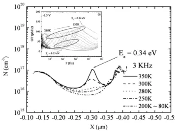
Incorporating N into the InGaAs cap layer of InAs QDs was previously shown to redshift the QD ground emission by reducing the potential barrier of the cap layer [12]. However, if a high concentration of N atoms are incorporated into the InAs QD layer, the carrier distribution in the QD changes from accumulation to depletion, suggesting the generation of a deep defect state. From cross-sectional transmission electron microscopy, lattice misfits are observed in the QD and neighboring GaAs layers. Thus, the N incorporation might lead to localized strain relaxation, and the deep defect state is tentatively assigned to be a strain-related lattice defect. Further investigation is needed to establish its detailed origin. The effect of this defect state on the carrier distribution near the QD is shown in figure1, which displays the capacitance–voltage (C–V ) depth profiles for N-incorporated InAs QDs deposited with a 2.4 ML thick InAs layer. Drastic electron depletion near the QD (at ∼0.3 μm) can be seen at T < 200 K, indicating that, at V = 0 V, the electrons in the QD are depleted by the defect state. The spatial distribution of the defect state can be probed by increasing the temperature to shorten the electron-emission time, allowing for the ac modulation of the trapped electrons on the defect state. As is seen, for T > 300 K and at a low frequency of 3 kHz, a broad peak (with a large linewidth of ∼50 nm) with long tails on both sides emerges. Because the height of the QD is only∼10 nm, the long tail suggests that the defect state extends from the QD into the neighboring GaAs layers. This temperature-dependent dispersion reflects a very long emission time, characteristic of electron emission from the defect state, rather than from the confinement states of the QDs. We obtain the emission times of the dispersion by measuring the conductance/frequency–frequency (G/F–F) spectra at the capacitance plateau corresponding to the broad peak, as shown in the inset of figure 1. A dominant peak E1 with emission energy (capture cross sectionσ) of 0.34 eV
(4.16 × 10⁻¹⁶ cm2) is obtained from typical Arrhenius plots.
Figure 1.C–V depth profiles of the N-incorporated InAs QDs,
illustrating temperature-dependent dispersion near the QD. The emission time of the dispersion is determined from the G/F–F spectra shown in the inset, illustrating two peaks at 0.34 and 0.15 eV, respectively.
These emission parameters are similar as those of the defect states associated with lattice misfits in strain-relaxed InAs QD [10,14,15] and InGaAs/GaAs heterostructures [16], and the emission energy was identified as relative to the GaAs CB [14]. Thus, N incorporation induces a localized strain-related lattice defect at 0.34 eV below the GaAs CB. This defect state lies below the QD electron GS and depletes electrons in the QD. Beside this defect, the G/F spectra in the inset of figure 1 show another weak emission E2 with emission energy (capture cross section) of 0.15 eV (σ = 1.46×10⁻¹⁸cm2). The origin of this emission is either another defect state or a QD electron state.
In order to establish its origin, we performed post-growth rapid thermal annealing on the sample. Figure 2 compares the depth profiles before and after annealing at 700◦C for 2 min, 800◦C for 3 min, and 800◦C for 5 min, respectively. Certain temperatures and frequencies were selected for the measurements in order to see the peaks clearly. For clarity, the curves are vertically shifted. For the as-grown samples, a high temperature of 350 K was selected to activate the defect emission E1 at 0.34 eV. The weak emission E2 at 0.15 eV is indicated at a depth from the voltage it is observed at in the
G/F spectra. This E2 emission is attributed to an emission
from the QD state for the following discussions. Annealing at 700◦C can weaken the defect emission E1 and enhance the QD emission E2. The emission energies are obtained to be 0.25 and 0.14 eV for E1 and E2, respectively. Both the defect and QD emission times are found to decrease after annealing. Lowering the temperature to 230 K is needed to resolve the QD emission from the defect emission. Annealing at 800◦C for 3 min further diminishes the defect emission, and after annealing at 800◦C for 5 min the defect emission becomes nearly invisible and the depth profile is left with only the QD emission with a very narrow linewidth. This evolution suggests a removal of the defect emission E1 and a recovery of the QD emission E2 after annealing. The carrier recovery in the QD 2
Figure 2. The carrier distributions of the N-incorporated InAs QDs before annealing and after annealing at 700◦C for 2 min, 800◦C for 3 min, and 800◦C for 5 min, respectively. Annealing can remove the defect state E1 and enhance the shallow emission E2.
can also be seen from the change in the valley concentration near the QD. The deepest valley concentration (at ∼250 K) increases from 7×1015cm−3before annealing to 1×1016cm−3 after annealing at 700◦C for 2 min, and to 2× 1016cm−3after annealing at 800◦C for 5 min. Since the carrier recovery in the QD is accompanied by an enhancement of E2 emission, E2 is considered as an emission from the QD state, rather than from another defect which is expected to be annealed out. The narrow linewidth (∼12 nm) of the QD emission after annealing at 800◦C for 5 min is consistent with a narrow QD layer (a typical dot height of∼10 nm).
For the as-grown samples, the emission energy (0.15 eV) of E2 is close to 0.14 eV reported by Brunkov et al [9] and 0.19 eV by Kapteyn et al [6] for the InAs QD GS with respect to the GaAs CB (emitting at∼1.0 eV). Thus, E2 is considered as an electron emission from the GS to the GaAs CB or a level close to the GaAs CB. By subtracting this emission energy (0.15 eV) and the PL emission energy (1.03 eV) of the QDs (to be shown) from the GaAs bandgap of 1.42 eV, we obtain the confinement energy of the hole ground state to be 0.24 eV. This energy is close to the reported value of 0.205 eV by Brunkov
et al [9], suggesting comparable confinement energies for the QD electron and hole ground states. We have compared our result with those obtained from capacitance spectroscopy. Let us compare to the data from optical absorption measurements.
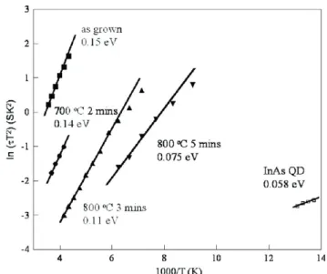
Figure 3. Arrhenius plots of the emission times of the shallow emission E2 before annealing and after annealing at 700◦C for 2 min, 800◦C for 3 min, and 800◦C for 5 min, respectively. The emission times of InAs QDs without N incorporation are also shown for comparison. Increasing the annealing temperature can decrease the emission time and energy.
Adawi et al [17] reported an energy of 0.17 eV for the transition from the QD electron GS to the wetting layer, which is very close to our value of 0.15 eV. Since the lowest-lying state in the wetting layer is about 50 meV below the GaAs CB, we cannot exclude the possibility that our obtained 0.15 eV emission is the electron emission from the QD electron GS to the wetting layer, rather than directly to the GaAs CB. If this is true, the QD electron GS is at about 0.20 eV below the GaAs CB edge, which is consistent with the data from Kapteyn
et al [6]. Furthermore, Raghavan et al [18] have reported a minimum binding energy of 0.21 eV for the QD electron GS based on an argument that the binding energy of the electron GS is higher than that of the hole GS. Accordingly, the values from the optical measurements are about 50 meV larger than our obtained value of 0.15 eV. Thus, it is possible that the observed electron emission by time-resolved capacitance spectroscopy is relative to the wetting layer, rather than the GaAs CB, leading to a reduction of about 50 meV. Further investigation is needed to make a more conclusive argument on this matter. For the time being, E2 is considered as an electron emission from the GS to the GaAs CB or to the wetting layer.
Figure3summarizes the Arrhenius plots of the emission times of the QD emission E2. In order to see the effect of the defect state on the QD emission, the emission times (indicated as ‘InAs QD 0.058 eV’) observed in the InAs QDs without N incorporation are also included (to be discussed). This emission time corresponding to the electron emission from the QD GS to the first excited state is very short and could only be resolved at a very low temperature. N incorporation significantly elongates the QD emission time. As is seen, the as-grown sample has the longest emission time. Annealing can significantly shorten the emission time. For example, the emission time (at 240 K) is 3× 10⁻⁵, 6× 10⁻⁶, and 8× 10⁻⁷s for samples as-grown, and after annealing at 700◦C for 2 min,
Nanotechnology 19 (2008) 495201 J F Chen et al
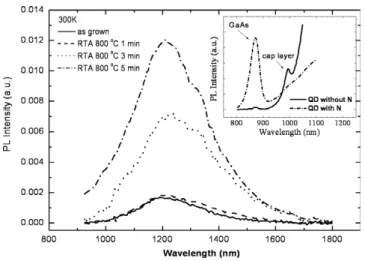
Figure 4. Room-temperature PL spectra for the as-grown
N-incorporated InAs QDs and after annealing at 800◦C for 1, 3, and 5 min, respectively. A weak broad emission from the QDs, centered at around 1200 nm, can be seen. Annealing can improve the emission without affecting the peak energy. The inset shows 300 K PL emissions (870 nm) of the GaAs layers for the N-free InAs QDs and the as-grown N-incorporated InAs QDs.
and annealing at 800◦C for 3 min, respectively. This emission time decrease is related to the decreasing emission energy from 0.15 eV for the as-grown sample, to 0.14 eV after 700◦C annealing for 2 min, to 0.11 eV (0.098–0.116 eV depending upon reverse voltage) after 800◦C annealing for 3 min, and to 0.075 eV (0.067–0.098 eV) after 800◦C annealing for 5 min. One possible reason for this decreasing emission energy is the upward energy shift of the QD state due to annealing-induced interdiffusion of atoms at the QD interface. However, no apparent blueshift which is usually attributed to the interdiffusion is observed in N-incorporated InAs QDs even after annealing up to 900◦C. Figure4shows the room-temperature PL spectra for the as-grown sample and samples after annealing at 800◦C for 1, 3 and 5 min, respectively. A weak broad PL spectra peaked at around 1200 nm originated from the QD is observed for the as-grown sample. The N incorporation significantly weakens the QD emission and causes a long low-energy tail. The degradation of the emission efficiency can be correlated with the drastic carrier depletion in the QD due to the defect state, which protrudes the conduction band near the QD and produces an energy barrier. This barrier can prevent the photo-generated carriers in the GaAs layers from falling into the QDs. This argument is supported by an observation of a rather strong emission (at 870 nm) from the GaAs layers in comparison with the N-free InAs QDs, as shown in the inset of figure 4. Annealing at 800◦C for 3 min can improve the PL emission from the QD and diminish the emission from the GaAs layers, consistent with a lowering of the energy protrusion due to the recovery of the carriers in the QD. As is seen, the peak energy of the QD PL emission displays no apparent shift (no shift is observed even after 900◦C annealing), suggesting that N incorporation may even suppress the interdiffusion. However, annealing may introduce a slight composition fluctuation since an additional weak bump at∼1330 nm can be seen. In view of the constant
Figure 5. The carrier distribution and PL spectra (in the inset) for N-free InAs/InGaAs QDs with InAs deposition thickness of 2.4 ML. The carrier distribution displays a strong peak at 0.225 μm with a right shoulder bump at 0.25 μm (indicated by an arrow). The strong peak is attributed to electrons tunneling from the QD excited states to the GaAs conduction band and the shoulder bump is attributed to a thermal excitation from the QD ground state to the first excited state and subsequent tunneling to the GaAs conduction band.
PL peak energy, we believe that the energy position of the QD state remains unchanged after annealing. From these PL spectra, the change of the observed emission energy for the QD emission cannot originate from an upward energy shift of the QD state. We attribute this change to a modification of tunneling emission in the QD excited states due to the defect state E1.
The N incorporation can significantly elongate the emission time of the QD state. This feature provides strong evidence for the effect of the defect state. To illustrate this, figure5shows the carrier profile and PL spectra (in the inset) of N-free InAs/InGaAs QDs with InAs deposition thickness of 2.4 ML. Without N incorporation, the QDs emit at 1300 nm at 300 K. The N incorporation causes a blueshift to 1200 nm. The detailed reason for this blueshift is not clear, but is suspected to be the result of strain relaxation in the QDs since lattice misfits are observed near the QD. Strain relaxation in the InAs QDs was previously shown to cause a sudden blueshift of 78 meV when the InAs deposition thickness exceeds a critical thickness of 3 ML [19]. This result shows that the N incorporation causes an upward energy shift of the QD electron state, which would reduce the emission time and energy. However, the experimental data show an opposite trend, excluding the energy shift of the QD state as the reason for the emission time elongation. Hence, the significant elongation of the emission time and energy can only be interpreted by the change of the emission process induced by the defect state.
The emission process for defect-free QDs is illustrated by the depth profile of the N-free QDs in figure5. The profile displays a strong peak at 0.225 μm with a right shoulder bump at 0.25 μm (indicated by an arrow). The shoulder bump becomes apparent at low temperatures. These depths are smaller than the depth of the QDs (0.3 μm), which is due to the fact that this sample was slightly chemically etched 4
before Schottky metal evaporation. The strong peak whose emission is too short to be resolved is attributed to electrons tunneling [9–11] from the QD excited states to the GaAs conduction band. The shoulder bump displays frequency-dependent attenuation with emission energy of∼58 meV [10]. Since this energy is comparable to the PL energy spacing between the ground and first excited peaks, the shoulder bump is attributed to a thermal excitation from the QD ground state to the first excited state and subsequent tunneling to the GaAs conduction band, in a two-stage emission process previously described [6]. This shows a marked tunneling effect for the QD excited states in the N-free QDs.
4. Conclusion
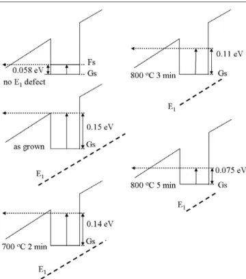
In view of the observed data, we summarize the likely emission processes in the CB schematic in figure6. Without the defect state, the electron emission is the previously identified two-step process [6]: from the GS to the FS with 0.058 eV and subsequent tunneling to the GaAs CB. The emission energy 0.058 eV corresponds to the energy separation between the GS and the FS. This emission process suggests a marked tunneling emission for the QD excited states. This emission time is very short, as indicated by ‘InAs QDs’ in figure 3. The N-induced defect state (indicated by a dashed line) can suppress the tunneling emission, presumably by inducing additional carrier depletion [11] and increasing the tunneling width (the detailed band structure is not shown). Electrons escaping out of the GS have to emit to a state near the GaAs CB, leading to a significant emission energy increase from 0.058 to 0.15 eV and several orders of magnitude increase in the emission time. The removal of the defect state by annealing would weaken the tunneling suppression, and thus electrons can escape out of the GS via a thermal emission to a state slightly lower, followed by tunneling to the GaAs CB. Increasing the annealing temperature further removes the defect state and enhances the trend. Since the QD excited states near the GaAs CB can be regarded as nearly continuous, a nearly monotonic decrease of the emission energy with increasing annealing temperature is expected. Figure 3shows that, for the cases of annealing at 800◦C for 3 and 5 min, the emission times bend toward weak temperature dependence at low temperatures, suggesting slightly decreasing emission energy at low temperature. This can be explained by a tunneling effect, and the electrons tunnel to the GaAs CB through a slightly lower QD state, further supporting the proposed tunneling suppression model.
In figure6, the dashed line we place in the QDs represents the energy at which the tunneling occurs for the electrons in the ground state out of the QDs. Except for the case of no E1 defect, this tunneling level does not represent any particular QD electron state. It is difficult to pinpoint the identity of this tunneling level. The N incorporation severely degrades the PL spectra. The PL spectra of the QD show only a very broad emission, rather than the distinguishable doublet ground and first excited transitions typically observed in N-free QDs (shown in the inset of figure 5). As already mentioned, the N incorporation might lead to strain relaxation in the QDs. The broadening of the PL spectra may be partly related to
Figure 6. Conduction-band schematic diagram for showing the emission of the electrons from the QD state. Without the N-induced defect state, electrons escaping out of the ground state (GS) occur via a thermal emission to the first excited state (FS) and subsequent tunneling to the GaAs CB, suggesting a significant tunneling for the QD excited states. With the defect state for suppressing tunneling, electrons are emitted from the GS to a state close to the GaAs CB. Annealing removes the defect state and weakens the tunneling suppression, leading to electrons escaping out of the GS via a lower state.
strain relaxation. This broadening makes it difficult to identify whether the tunneling level belongs to the QD first excited or higher states. For annealing at 800◦C for 5 min, the tunneling level is 75 meV above the QD electron GS. However, this 75 meV emission energy is obtained from the peak intensity of the G/F spectra. Actually, the emission energies are observed to be from 67 to 98 meV depending upon increasing dc voltages during the G/F measurements. Thus, the tunneling level is not a very sharp level; it consists of a band with a broadness of 31 meV. This emission energy is larger than the energy separation (58 meV) between the electron GS and first excited state observed from the N-free QDs, but is slightly smaller than the energy separation between the electron GS and the second excited state. From intraband transmission measurements, Adawi et al [17] have observed an absorption peak with 113 meV corresponding to a transition from the QD electron GS to second excited state. Thus, the 75 meV tunneling level is speculated to be either the electron first excited or second excited state. If it is the first excited state, the emission time should be close to those observed in the N-free QDs. However, figure3shows that the emission time is still much larger than those observed in the N-free QDs; thus we tend to speculate the tunneling level to be the second excited state. We have tried to increase the annealing temperature to 900◦C to see if the emission time can be further reduced
Nanotechnology 19 (2008) 495201 J F Chen et al to be close to those of the N-free QDs. Unfortunately, the
leakage current related to the annealing-induced damage on the sample surface renders electrical measurements impossible. As to other higher tunneling levels, we can not argue further about their identities, and thus, for the time being, regard them as continuous states.
Acknowledgments
The authors are grateful to Dr J Y Chi and R S Hsiao for sample preparation and to the National Science Council of the Republic of China, Taiwan for financially supporting this research under Contract No. NSC-95-2112-M-009-010. This work has also been supported by MOE, ATU program.
References
[1] Heinrichsdorff F, Mao M-H, Kirstaedter N, Krost A and Bimberg D 1997 Appl. Phys. Lett.71 22
[2] Eaglesham D J and Cerullo M 1990 Phys. Rev. Lett.64 1943 [3] Leonard D, Pond K and Petroff P M 1994 Phys. Rev. B
50 11683
[4] Guha S, Madhukar A and Rajkumar K C 1990 Appl. Phys. Lett. 57 2110
[5] Arakawa Y and Sakaki H 1982 Appl. Phys. Lett.40 939 [6] Kapteyn C M A, Heinrichsdorff F, Stier O, Heitz R,
Grundmann M and Werner P 1999 Phys. Rev. B60 14265
[7] Luyken R J, Lorke A, Govorov A O, Kotthaus J P, Medeiros-Riberro G and Petroff P M 1999 J. Appl. Phys. 74 2486
[8] Letartre X, Stievenard D and Lanoo M 1991 J. Appl. Phys. 69 7336
[9] Brunkov P N, Patane A, Levin A, Eaves L, Main P C,
Musikhin Yu G, Volovik B V, Zhukov A E, Ustinov V M and Knonnikov S G 2002 Phys. Rev. B65 085326
[10] Chen J F, Hsiao R S, Wang C K, Wang J S and Chi J Y 2005
J. Appl. Phys.98 013716
[11] Chen J F, Wang Y Z, Chiang C H, Hsiao R S, Wu Y H, Chang L, Wang J S, Chi T W and Chi J Y 2007
Nanotechnology18 355401
[12] Chen J F, Hsiao R S, Hsieh P C, Chen Y J, Chen Y P, Wang J S and Chi J Y 2005 J. Appl. Phys.98 113525 [13] Wang J S et al 2004 J. Vac. Sci. Technol. B22 2663 [14] Chen J F and Wang J S 2007 J. Appl. Phys.102 043705 [15] Chen J F, Hsiao R S, Huang W D, Wu Y H, Chang L,
Wang J S and Chi J Y 2006 Appl. Phys. Lett.88 233113 [16] Uchida Y, Kakibayashi H and Goto S 1993 J. Appl. Phys.
74 6720
[17] Adawi A M, Zibik E A, Wilson L R, Lemaitre A,
Cockburn J W, Skolnick M S, Hopkinson M and Hill G 2003
Appl. Phys. Lett.83 602
[18] Raghavan S, Rotella P, Stintz A, Fuches B, Krishna S, Morath C, Cardimora D A and Kennerly S W 2002
Appl. Phys. Lett.81 1369
[19] Chen J F, Hsiao R S, Chen Y P, Wang J S and Chi J Y 2005
Appl. Phys. Lett.87 141911