710 IEEE ELECTRON DEVICE LETTERS, VOL. 23, NO. 12, DECEMBER 2002
La
2
O
3
/Si
0:3
Ge
0:7
p-MOSFETs With High Hole
Mobility and Good Device Characteristics
C. H. Huang, S. B. Chen, and Albert Chin, Senior Member, IEEE
Abstract—We have studied the high- La2O3p-MOSFETs on Si0 3Ge0 7substrate. Nearly identical gate oxide current, capaci-tance density, and time-dependent dielectric breakdown (TDDB) are obtained for La2O3/Si and La2O3/Si0 3Ge0 7 devices that indicate the excellent Si0 3Ge0 7 quality without any side effect. The measured hole mobility in nitrided La2O3/Si p-MOSFETs is 31 cm2/V-s and comparable with published data in nitrided HfO2/Si p-MOSFETs. In sharp contrast, a higher mobility of 55 cm2/V-s is measured in La2O3/Si0 3Ge0 7p-MOSFET, which is improved by 1.8 times as compared with La2O3/Si control devices. The high mobility in Si0 3Ge0 7p-MOSFET gives another step for integrating high- gate dielectrics into VLSI process.
Index Terms—High- , hole mobility, La2O3, SiGe.
I. INTRODUCTION
A
LTHOUGH high- gate dielectrics [1]–[5] have been proposed for possibly replacing SiO or Si N , the smaller mobility in high- MOSFET is still an important con-cern that may reduce the required high on-state drive current ( ). The mobility degradation is greater in p-MOSFET than n-MOSFET because of the larger hole effective mass, which becomes more serious after surface nitridation but is needed for maintaining the small equivalent oxide thickness (EOT) during thermal cycle [2]. One method to improve the hole mobility is to use SiGe channel, but unfortunately, the conventional UHVCVD-grown SiGe faces the strain relaxation related poor surface, large junction leakage, and degraded MOSFET performance after subsequent thermal cycle [6]–[9]. Recently, we have developed a high-temperature stable SiGe process [10], and good gate oxide integrity, small silicide junction leakage current, higher hole mobility, and better p-MOSFET characteristics than Si counterparts have been demonstrated [11]–[14]. In this letter, we have further inte-grated the high-temperature stable SiGe with high- La O . We have achieved a hole mobility of 55 cm /V-s in nitrided La O /Si Ge p-MOSFET that is 1.8 times higher than the 31 cm /V-s mobility in nitrided La O /Si control p-MOSFET. The improved mobility is important to realize high- dielectric integration into VLSI technology.Manuscript received August 13, 2002; revised September 16, 2002. The re-view of this letter was arranged by Editor B. Yu.
The authors are with the Department of Electronics Engineering, Na-tional Chiao Tung University, Hsinchu 300, Taiwan, R.O.C. (e-mail: achin@cc.nctu.edu.tw).
Digital Object Identifier 10.1109/LED.2002.805749
II. EXPERIMENTAL
Standard 4-in (100) n-type Si wafers with 1 2 -cm resis-tivity (5 10 1 10 cm concentration) were used in this work. After device isolation and modified RCA clean, the amorphous Ge layer is selectively deposited on the active region. An HF-vapor passivation is used to suppress the native oxide formation before Ge deposition [10]–[14]. After rapid thermal annealing (RTA) at 900 C, a 350 Å single crystal Si Ge was formed by solid-phase epitaxy in the active region, as confirmed by X-ray diffraction, electron diffraction pattern, and cross-sectional transmission electron microscopy (TEM) [10]. The formed SiGe may be strain-relaxed, since it was formed at high temperature. Then, the source-drain p region was formed by implantation followed by a 950 C RTA [11]. The La O gate oxide of 60 Å was formed by de-positing La and oxidation and measured by ellipsometer. More detailed Si Ge and La O characterization can be found in our previous study [4], [5], [10]–[14]. Next, NH nitridation was performed at 550 C before gate electrode formation. The p-MOSFETs and MOS capacitors were fabricated using Al as gate electrode and characterized by – and – measurements. In addition to La O /Si Ge p-MOSFETs, La O /Si control devices were also fabricated as references.
III. RESULTS ANDDISCUSSION
Fig. 1(a) and (b) shows the – characteristics and cu-mulative time-dependent dielectric breakdown (TDDB) of both La O /Si Ge and La O /Si p-MOSFETs, respectively. The almost identical gate current suggests the Si Ge channel has little negative effect as compared with the Si case. The same gate current is due to nearly the same work function of Si and SiGe [15] and conduction band difference between La O and Si or SiGe. The comparable gate oxide integrity is also evidenced from the nearly identical TDDB for La O on Si or SiGe.
We have further measured the quasi-static and high-fre-quency (100 KHz) – characteristics of both La O /Si and La O /Si Ge p-MOSFETs and the results are shown in Fig. 2. The identical accumulation capacitance and the same small 10 meV hysteresis measured for both devices indicate that the using SiGe does not have any side effect. An EOT of 16 Å is measured with a leakage current of 1.5 10 A/cm at 1 V that is four orders of magnitude lower than SiO at the same EOT. The smaller flat band voltage in La O /Si Ge devices may be due to the smaller energy bandgap, which gives additional flexibility to tune .
HUANG et al.: La O /Si Ge p-MOSFETs WITH HIGH HOLE MOBILITY 711
Fig. 1. (a) Gate leakage current and (b) cumulative TDDB of La O /Si and La O /Si Ge p-MOSFETs under positive gate bias.
Fig. 2. C–V characteristics of La O /Si and La O /Si Ge MOS capacitors.
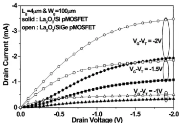
Fig. 3 shows the – characteristics of 4 m La O /Si and La O /Si Ge p-MOSFETs plotted at the same – . Al-though a relatively large junction leakage of 1 10 A/cm is measured, it can be lowered to 1 10 A/cm using Ni gemeno-silicide, which was used in our previous study [14]. In addition to the good device – characteristics, the Si Ge has 2 times higher current driving capability than the Si de-vice at the same of 2 V. Because the La O was formed
Fig. 3. I –V characteristics of La O /Si and La O /Si Ge p-MOSFETs.
Fig. 4. (a)I –V characteristics and (b) the hole mobility of La O /Si and La O /Si Ge p-MOSFETs.
on Si and Si Ge on the same lot with identical inversion capacitance in Fig. 2, the higher hole current is not due to the different gate dielectric. The significantly higher hole current is especially important for high-speed circuit application, which is the fundamental motivation for continuously scaling down.
Because the improved hole current may come from both higher mobility and threshold voltage ( ) difference, we have further measured the transfer – characteristics. Fig. 4(a)
712 IEEE ELECTRON DEVICE LETTERS, VOL. 23, NO. 12, DECEMBER 2002
and (b) shows the – and hole effective mobility for both La O /Si and La O /Si Ge p-MOSFETs, respectively, where the difference is also included for the mobility extraction. In addition to having a higher saturation hole current than La O /Si devices, the La O /Si Ge p-MOSFETs have the same off-state current ( ) and lower . The lower in the La O /Si Ge device is due to the smaller energy bandgap in Si Ge . In addition to the small difference of 0.2 V, the large hole current improvement is primary coming from the higher mobility using Si Ge . A peak hole mobility of 31 cm /V-s is obtained in the nitrided La O /Si p-MOSFET that is comparable with nitrided HfO /Si [2]. In sharp contrast, the La O /Si Ge device has a higher hole mobility of 55 cm /V-s that is 1.8 times higher than the La O /Si control devices without using SiGe. In addition to the comparable gate oxide integrity and , the higher mobility and indicate that the superior device performance can be realized in nitrided high- La O p-MOSFETs using solid-phase epitaxy formed SiGe.
IV. CONCLUSION
In addition to the almost identical gate oxide leakage current, capacitance density, TDDB, and , we have achieved a 2 times higher and high hole mobility of 55 cm /V-s in nitrided La O /Si Ge p-MOSFETs. The improved hole mobility in the La O /Si Ge p-MOSFET gives another step to realize high- gate dielectrics for VLSI integration.
ACKNOWLEDGMENT
The authors would like to thank P. Mei from GlobiTech for the help and support.
REFERENCES
[1] Y. H. Kim, C. H. Lee, T. S. Jeon, W. P. Bai, C. H. Choi, S. J. Lee, L. Xinjian, R. Clarks, D. Roberts, and D. L. Kwong, “High-quality CVD TaN gate electrode for sub-100–nm MOS devices,” in IEDM Tech. Dig., 2001, pp. 667–670.
[2] K. Oishi, C. S. Kang, R. Choi, H.-J. Cho, S. Gopalan, R. Nieh, E. Dhar-marajan, and J. C. Lee, “Reliability characteristics, including NBTI, of polysilicon gate HfO MOSFETs,” in IEDM Tech. Dig., 2001, pp. 659–662.
[3] D. A. Buchanan, E. P. Gusev, E. Cartier, H. Okorn-Schmidt, K. Rim, M. A. Gribelyuk, A. Mocuta, A. Ajmera, M. Copel, S. Guha, N. Bojarczuk, A. Callegari, C. D’Emic, P. Kozlowski, K. Chan, R. J. Fleming, P. C. Jamison, I. Brown, and R. Arndt, “80-nm polysilicon gated n-FETs with ultrathin Al O gate dielectric for ULSI applications,” in IEDM Tech. Dig., 2000, pp. 223–226.
[4] A. Chin, C. C. Liao, C. H. Lu, W. J. Chen, and C. Tsai, “Device and reliability of high-k Al O gate dielectric with good mobility and low
D ,” in Symp. VLSI Technology, 1999, pp. 135–136.
[5] A. Chin, Y. H. Wu, S. B. Chen, C. C. Liao, and W. J. Chen, “High-quality La O and Al O gate dielectrics with equivalent oxide thickness 5–10 Å,” in Symp. VLSI Technology, 2000, pp. 16–17.
[6] Y. Taur and T. K. Ning, Fundamentals of Modern VLSI De-vices. Cambridge, U.K.: Cambridge Univ. Press, 1998, p. 286. [7] S. Verdonckt-Vandebroek, E. F. Crabbe, B. S. Meyerson, D. L. Harame,
P. J. Restle, J. M. C. Stork, and J. B. Johnson, “SiGe-channel heterojunc-tion p-MOSFETs,” IEEE Trans. Electron Devices, vol. 41, pp. 90–101, Jan. 1994.
[8] R. S. Prassad, T. J. Thornton, S. Kanjanachuchai, J. Fernandez, and A. Matsumura, “Mobility degradation in gated Si: SiGe quantum wells with thermally grown oxide,” Electron. Lett., vol. 31, no. 21, pp. 1876–1878, 1995.
[9] K. Goto, J. Murota, T. Maeda, R. Schutz, K. Aizawa, R. Kircher, K. Yokoo, and S. Ono, “Fabrication of a Si Ge channel metal–oxide-semiconductor field-effect transistor (MOSFET) con-taining high Ge fraction layer by low-pressure chemical vapor deposition,” Jpn. J. Appl. Phys., vol. 32, no. 1B, pp. 438–441, 1993. [10] Y. H. Wu, W. J. Chen, A. Chin, and C. Tsai, “The effect of native oxide on
epitaxial SiGe from deposited amorphous Ge on Si,” Appl. Phys. Lett., vol. 74, no. 4, pp. 528–530, 1999.
[11] Y. H. Wu and A. Chin, “High-temperature formed SiGe p-MOSFETs with good device characteristics,” IEEE Electron Device Lett., vol. 21, pp. 350–352, July 2000.
[12] , “Gate oxide integrity of thermal oxide grown on high temperature formed Si Ge ,” IEEE Electron Device Lett., vol. 21, pp. 113–115, Mar. 2000.
[13] Y. H. Wu, A. Chin, and W. J. Chen, “Thickness-dependent gate oxide quality of thin thermal oxide grown on high-temperature formed SiGe,” IEEE Electron Device Lett., vol. 21, pp. 289–291, June 2000. [14] C. Y. Lin, W. J. Chen, C. H. Lai, A. Chin, and J. Liu, “Formation of
Ni germano-silicide on single crystalline Si Ge /Si,” IEEE Electron Device Lett., vol. 23, no. 8, pp. 464–466, 2002.
[15] C. Salm, J. H. Klootwjik, Y. Ponomarev, P. W. M. Boos, D. J. Gravestejin, and P. H. Woerlee, “Gate current and oxide reliability in p poly MOS capacitors with poly-Si and poly-Si Ge ,” IEEE Electron Device Lett., vol. 19, pp. 213–215, July 1998.