Soft breakdown enhanced hysteresis effects in ultrathin oxide silicon-on-insulator
metal-oxide-semiconductor field effect transistors
M. C. Chen, S. H. Ku, C. T. Chan, and Tahui Wang
Citation: Journal of Applied Physics 96, 2297 (2004); doi: 10.1063/1.1773384
View online: http://dx.doi.org/10.1063/1.1773384
View Table of Contents: http://scitation.aip.org/content/aip/journal/jap/96/4?ver=pdfcov Published by the AIP Publishing
Articles you may be interested in
Origin of the front-back-gate coupling in partially depleted and fully depleted silicon-on-insulator metal-oxide-semiconductor field-effect transistors with accumulated back gate
J. Appl. Phys. 98, 114506 (2005); 10.1063/1.2138380
Comparison of oxide breakdown progression in ultra-thin oxide silicon-on-insulator and bulk metal-oxide-semiconductor field effect transistors
J. Appl. Phys. 96, 3473 (2004); 10.1063/1.1776640
Electron valence-band tunneling-induced Lorentzian noise in deep submicron silicon-on-insulator metal–oxide–semiconductor field-effect transistors
J. Appl. Phys. 94, 4461 (2003); 10.1063/1.1604452
Enhanced electroluminescence in silicon-on-insulator metal–oxide–semiconductor transistors with thin silicon layer
Appl. Phys. Lett. 82, 4830 (2003); 10.1063/1.1587877
Low-frequency noise overshoot in ultrathin gate oxide silicon-on-insulator metal–oxide–semiconductor field-effect transistors
Appl. Phys. Lett. 82, 1790 (2003); 10.1063/1.1561575
silicon-on-insulator metal-oxide-semiconductor field effect transistors with an ultrathin oxide
共1.6 nm兲 is investigated. Two breakdown enhanced hysteresis modes are identified. In a drain-edge
breakdown device, excess holes result from band-to-band tunneling flow to the floating body, thus causing threshold voltage variation in drain bias switching. In contrast, in a channel breakdown device, enhanced threshold hysteresis is observed during gate bias switching because of increased valence band electron tunneling. Our findings reveal that soft breakdown enhanced hysteresis effect can be a serious reliability issue in silicon-on-insulator devices with floating body configuration. © 2004 American Institute of Physics.[DOI: 10.1063/1.1773384]
I. INTRODUCTION
Silicon-on-insulator(SOI) technology has emerged as a promising technology for system-on-a-chip applications, which require high-performance complementary metal-oxide-semiconductor field effect transistors(MOSFET), low power, embedded memory, and bipolar devices. The primary feature of a MOSFET with SOI configuration is that the local substrate of the device is floating electrically, and thus the substrate-source bias共VBS兲 is not fixed. As VBSchanges, the
device threshold voltage 共Vt兲 will change due to the body effect. This “instability” in Vt resulting from floating body configuration becomes one of the most challenging tasks in bringing SOI devices into mainstream applications.1–4 One manifestation of the Vtvariation is the hysteresis effect. The Vt hysteresis as a result of various floating body charging/ discharging mechanisms has been widely investigated.2–4In this work, the influence of gate oxide breakdown position on hysteresis effects in ultrathin oxide partially-depleted (PD) SOI MOSFETs will be explored.
Several causes of Vt hysteresis in PD SOI MOSFETs have been proposed.5–8Boudou et al.5 reported that Vt hys-teresis could be caused by positive feedback of impact ion-ization due to long time constants associated with body po-tential charging. Chen et al.6showed that at high drain biases the floating body effect can lead to hysteresis in the sub-threshold Ids– Vgscharacteristics even when the gate is biased
well below its threshold voltage. Fung et al.7 found that in ultrathin gate oxide devices the gate-to-body tunneling cur-rent modulates the body voltage and induces a hysteresis effect. All the above works investigate the hysteresis phe-nomenon in PD SOI MOSFETs without considering gate ox-ide soft breakdown(SBD). Recent studies9–13showed that in bulk CMOS the impact of gate oxide SBD is only manifested in a noticeable increase in gate leakage current without de-grading other device characteristics in operation. Crupi et al.14 showed that at high gate voltages the substrate current
steeply increases after SBD due to localized effective thin-ning of gate oxide. Chan et al.15 presented that in thinner oxides the post-SBD gate induced drain leakage(GIDL) cur-rent increases significantly because of the enhancement of band-to-band tunneling. Although the dependence of these excess substrate currents on the location of a SBD spot was widely explored, the influence of SBD location on Vt hyster-esis in SOI devices has been rarely investigated.
II. DEVICE STRUCTURE AND CHARACTERIZATION
The devices in this work were made with a 0.13m standard CMOS process on p-type PD SOI substrate. The gate oxide was grown with rapid plasma nitridation (RPN) process. The gate length is 0.13m, the gate width is 10m and the oxide thickness is 1.6 nm. The test devices have an H-gate structure with an additional contact to facilitate the measurement of the body current and voltage. In this paper, all devices were stressed at high constant gate voltage with the source and drain grounded. The stress was stopped im-mediately after the first breakdown was detected. The current compliance for breakdown detection was chosen to be 10A. After breakdown, the device on-state characteristics were checked and no difference was observed.
a)Electronic mail: [email protected]
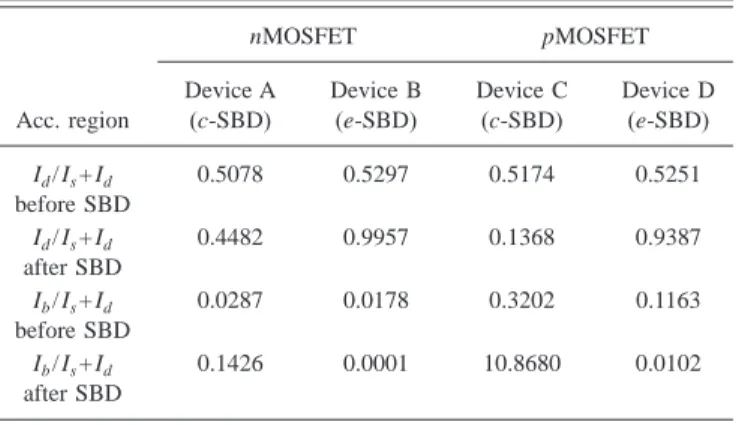
TABLE I. The ratio of Id/共Is+ Id兲 and Ib/共Is+ Id兲 before and after soft
break-down in four SOI MOSFETs. The measurement is in the accumulation re-gion and Vg=兩1.5 V兩, Vd= Vs= 0 V. Acc. region nMOSFET pMOSFET Device A (c-SBD) Device B (e-SBD) Device C (c-SBD) Device D (e-SBD) Id/ Is+ Id before SBD 0.5078 0.5297 0.5174 0.5251 Id/ Is+ Id after SBD 0.4482 0.9957 0.1368 0.9387 Ib/ Is+ Id before SBD 0.0287 0.0178 0.3202 0.1163 Ib/ Is+ Id after SBD 0.1426 0.0001 10.8680 0.0102
0021-8979/2004/96(4)/2297/4/$20.00 2297 © 2004 American Institute of Physics
The breakdown position was examined by using the method proposed by Degraeve et al.16Table I shows the ratio of Id to 共Is+ Id兲 before and after SBD in four SOI devices. The measurement is in accumulation region and兩Vg兩=1.5 V and Vd= Vs= 0 V. A significant increase of Id/共Is+ Id兲 in de-vice B and dede-vice D indicates that breakdown is located at the drain edge, while in device A and device C the moderate change in Id/共Is+ Id兲 implies that the SBD position is in the channel. Aside from Id/共Is+ Id兲, Ib/共Is+ Id兲 was measured
(also shown in Table I). In the channel SBD (c-SBD)
de-vices, the valence band tunneling leakage in the channel re-gion 共Ib兲 was enhanced, resulting in a larger Ib/共Is+ Id兲. In the case of edge SBD(e-SBD), the breakdown was above the drain edge. As a result, the tunneling leakage current in the channel region remains almost the same as in pre-SBD, and the increased edge leakage current makes Is+ Id larger and thus a smaller Ib/共Is+ Id兲. In short, the results in Table I shows that we can use the change of Id/共Is+ Id兲 or Ib/共Is + Id兲 to determine the breakdown location in the channel or in the drain edge region.
By utilizing the above technique, the device electrical behavior in c-SBD and e-SBD devices were characterized. In Fig. 1, the gate current and the substrate current as a function of Vg in a fresh, c-SBD, and an e-SBD nMOSFET were compared. The result shows that the substrate current in-creases drastically after c-SBD, but has little change after e-SBD. The substrate current at a positive gate bias is attrib-uted to valence electron tunneling from the channel to the gate. The generated holes left behind in the channel then flow to the substrate. This tunneling process is unlikely to occur in the n+drain region since the valence-band edge of
the n+drain is aligned with the band gap of the n+poly-gate.
Thus, Ibis enhanced significantly at a positive gate bias in a c-SBD device due to localized effective oxide thinning14,17,18 while Ib in an e-SBD device is nearly unchanged. Figure 2 shows the drain bias dependence of the GIDL current before and after SBD. The substrate current has an apparent in-crease after edge SBD. This is because at a high drain bias the Ib comes from electron band-to-band tunneling in the drain depletion region and the generated holes flow to the substrate. Since the electrical field in the drain region be-comes stronger after e-SBD due to effectively oxide thin-ning, the GIDL 共Ib兲 in an e-SBD device is enhanced. The same phenomena in p-MOSFETs are also observed and the result is shown in Fig. 3.
III. MODES OF SBD ENHANCED HYSTERESIS
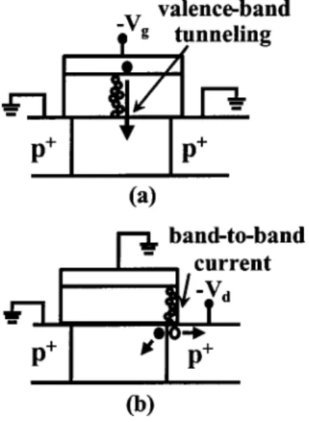
Two modes of SBD enhanced body potential alteration are proposed. Figure 4 illustrates two floating-body charging processes in c-SBD and in e-SBD SOI nMOSFETs.19,20In a c-SBD device with a positive gate bias [Fig. 4(a)], valence band electron tunneling from the channel to the gate is in-creased after SBD. The generated holes flow to the body and raise the body potential. Figure 4(b) shows the drain-induced floating-body charging in an e-SBD nMOSFET. Since the
FIG. 2. Body current versus drain bias in nMOSFETs. Solid line refers to an unstressed device and dashed line(dotted line) refers to a device after chan-nel SBD(drain edge SBD).
FIG. 1. Gate current and substrate current versus gate bias in nMOSFETs. Solid line refers to an unstressed device and dashed line(dotted line) refers
to a device after channel SBD(drain edge SBD).
FIG. 3. Gate current and substrate current versus gate bias in pMOSFETs. Solid line refers to an unstressed device and dashed line(dotted line) refers to a device after channel SBD(drain edge SBD).
FIG. 4. Illustration of two soft-breakdown enhanced floating-body charging processes in SOI nMOSFETs.(a) Soft breakdown in the channel region and hole creation due to valence band electron tunneling;(b) soft breakdown in the drain region and enhanced GIDL current.
2298 J. Appl. Phys., Vol. 96, No. 4, 15 August 2004 Chenet al.
breakdown path is in the drain edge, the GIDL current in-creases due to a stronger band bending in the n+drain region,
thus raising the body potential at a high drain bias. On the contrary, the GIDL current does not change in a c-SBD de-vice. Likewise, Fig. 5 shows two possible floating-body charging processes in pMOSFETs. Due to the above two charging processes, we conclude that the body potential of both nMOSFET and pMOSFET can be modified either dur-ing gate switchdur-ing or durdur-ing drain switchdur-ing dependdur-ing on the location of a SBD spot.
IV. RESULTS AND DISCUSSION
Figure 6 shows the Ids– Vgs hysteresis in a PD SOI
nMOSFET before and after c-SBD. The measurement drain bias is 0.1 V. The gate bias is swept from 0 V to 1.3 V and then is reversely swept from 1.3 to 0 V. Note that (i) the subthreshold hysteresis before SBD is insignificant and (ii) the post-SBD hysteresis is induced by gate bias sweep in this device. The corresponding body potential fluctuation in gate bias sweep is shown in Fig. 6. The arrow in the figure indi-cates the direction of bias sweep. After c-SBD, the body potential begins to rise when the Vg amplitude is above 0.8 V. The gate switching induced body potential variation
can be as large as 0.3 V in this case. The pre-SBD body potential hysteresis at the same switching amplitude is less than a few tens of millivolts. The c-SBD induced Vt hyster-esis is also observed in a pMOSFET. The measurement data are not shown here.
In an e-SBD device, although gate enhanced hysteresis is not observed, drain sweep induced hysteresis in subthresh-old leakage current is remarkable(Fig. 7). In this figure, the measurement Vgs is 0 V and the drain bias is swept from
0 V to 1.3 V and then reversely swept back. The body po-tential variation is shown in Fig. 7, too. The e-SBD enhanced hysteresis effect is clearly shown in this figure. It should be noted these breakdown-induced hysteresis effects occurs in off-state rather than in on-state where hot carrier impact ion-ization has been reported as a responsible charging mechanism.5
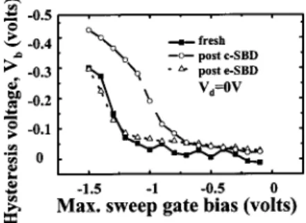
The relationship between the magnitude of sweep volt-age and the body potential hysteresis in the two SBD modes is investigated. In nMOSFETS, the degree of hysteresis in terms of the body potential variation versus the amplitude of the sweep voltage is shown in Fig. 8 for gate bias sweep and FIG. 7. Hysteresis in subthreshold current and corresponding floating-body potential in an e-SBD SOI nMOSFETs. Measurement is performed with forward and then reverse drain sweeps from 0 V to 1.3 V.
FIG. 8. The variation of body voltage Vbas a function of the amplitude of
gate bias sweep in SOI nMOSFETs. Vd= 0 V.
FIG. 9. The variation of body voltage Vbas a function of the amplitude of
drain bias sweep in SOI nMOSFETs. Vg= 0 V.
FIG. 5. Illustration of two soft-breakdown enhanced floating-body charging processes in SOI pMOSFETs.(a) Soft breakdown in the channel region and valence band electron tunneling from poly-gate to the floating body;(b) soft
breakdown in the drain region and enhanced GIDL current.
FIG. 6. Hysteresis in Idsand corresponding floating-body potential versus Vg
in a c-SBD SOI nMOSFETs. Measurement is performed with forward and then reverse drain sweeps from 0 V to 1.3 V.
in Fig. 9 for drain bias sweep. The hysteresis voltage is de-fined as the maximum substrate charging voltage during the sweep. In gate bias sweep(Fig. 8), the c-SBD device shows an increased hysteresis voltage while the hysteresis voltage of the e-SBD device is almost unchanged. In contrast, the e-SBD device shows a larger hysteresis voltage in drain bias sweep (Fig. 9). Similar results in pMOSFETs are presented in Fig. 10 for gate bias sweep and in Fig. 11 for drain bias sweep. From our characterization, we found SBD induced hysteresis effect may become appreciable even when the supply voltage is below 0.8 V.
The impact of SBD enhanced body charging effect in CMOS operation is described as follows. Figure 12 illus-trates the dominant Vt hysteresis modes in a SOI CMOS inverter. Hot carrier (HC) induced floating body charging occurs in on-state1,5 and it is dominant only when the in-verter is during switching. On the other hand, floating body charging takes place in c-SBD (e-SBD) nMOSFETs and e-SBD(c-SBD) pMOSFETs when the input signal is at high
(low) state. Since the soft breakdown induced body charging
is in the off-state, the time for charging can be much longer than the on-state HC caused body charging. Our study re-veals that SBD in PD SOI MOSFETs not only increases leakage current but also affects circuit stability.
V. CONCLUSIONS
The significance of soft breakdown position to Vt hyster-esis in PD SOI CMOS devices has been evaluated. Two SBD enhanced hysteresis modes in off-state CMOS are identified. The dominant floating body charging mechanism is valence band tunneling in c-SBD devices and band-to-band tunneling
in e-SBD devices. The SBD enhanced hysteresis effect may occur even with supply voltage less than 1.0 V and would be a serious reliability concern in ultrathin oxide PD SOI cir-cuits.
ACKNOWLEDGMENTS
The authors would like to acknowledge financial support from NSC, Taiwan under Contract No. NSC92-2215-E009-024. Device preparation by UMC is gratefully acknowl-edged.
1
T. Ouisse, G. Ghibaudo, J. Brini, S. Cristoloveanu, and G. Borel, J. Appl. Phys. 70, 3912(1991).
2
A. Wei, M.J. Sherony, and D.A. Antoniadis, IEEE Trans. Electron Devices
45, 430(1998).
3
J. Pretet, N. Subba, Dimitris Ioannou, Sorin Cristoloveanu, W. Maszara, and C. Raynaud, IEEE Electron Device Lett. 23, 300(2002).
4
T. Poiroux, O. Faynot, C. Tabone, H. Tigelaar, H. Mogul, N. Bresson, and S. Cristoloveanu, IEEE International SOI Conference 99(2002).
5
Alain Boudou and Brian Doyle, IEEE Electron Device Lett. 8, 300
(1987).
6
C.-E. Daniel Chen, Mishel Matloubian, and R. Sundaresan, IEEE Electron Device Lett. 9, 636(1988).
7
S.K. H. Fung, N. Zamdmer, P.J. Oldiges, J. Sleight, A. Mocuta, M. Sherony, S-H. Lo, R. Joshi, C.T. Chuang, I. Yang, S. Crowder, T.C. Chen, F. Assaderaghi, and G. Shahidi, Tech. Dig. - Int. Electron Devices Meet.
2001, 231. 8
Ruchir Puri, C.T. Chang, Mark B. Ketchen, Mario M. Pelella, and Michael G. Rosenfield, IEEE J. Solid-State Circuits 36, 290(2001).
9
Eli Harari, J. Appl. Phys. 49, 2478(1978).
10
I.C. Chen, S. Holland, K.K. Young, C. Chang, and C. Hu, Appl. Phys. Lett. 49, 669(1986).
11
M. Houssa, T. Nigam, P.W. Mertens, and M.M. Heyns, J. Appl. Phys. 84, 4351(1998).
12
E. Miranda, J. Sune, R. Rodriguez, M. Nafria, and X. Aymerich, Appl. Phys. Lett. 73, 490(1998).
13
B.E. Weir, P.L. Silverman, D. Monroe, K.S. Krisch, M.A. Alam, G.B. Alers, T.W. Sorsch, G.L. Timp, F. Baumann, C.T. Liu, Y. Ma, and D. Hwang, Tech. Dig. - Int. Electron Devices Meet. 1997, 73.
14
Felice Crupi, Giuseppe Iannaccone, Isodiana Crupi, Robin Degraeve, Guido Groeseneken, and Herman E. Mase, IEEE Trans. Electron Devices
48, 1109(2001).
15
T.Y. Chan, J. Chen, P.K. Ko, and C. Hu, Tech. Dig. - Int. Electron Devices Meet. 1987, 718.
16
Robin Degraeve, Ben Kaczer, An De Keersgieter, and Guido Groe-seneken, Proc. Int. Reliab. Phys. Symp. 360(2001).
17
J.H. Stathis, J. Appl. Phys. 86, 5757(1999).
18
Enrique Miranda and Jordi Sune, Appl. Phys. Lett. 78, 225(2001).
19
E. Wu, E. Nowak, J. Aitken, W. Abadeer, L.K. Han, and S. Lo, Tech. Dig. - Int. Electron Devices Meet. 1998 187.
20
M.C. Chen, C.W. Tsai, S.H. Gu, Tahui Wang, S. Huang Lu, S.W. Lin, G.S. Yang, J.K. Chen, S.C. Chien, Y.T. Loh, and F.T. Liu, Proc. Int. Reliab. Phys. Symp. 404(2002).
FIG. 12. Illustration of dominant Vthysteresis modes in the switching of an
SOI CMOS inverter. FIG. 10. The variation of body voltage Vbas a function of the amplitude of
gate bias sweep in SOI pMOSFETs. Vd= 0 V.
FIG. 11. The variation of body voltage Vbas a function of the amplitude of
drain bias sweep in SOI pMOSFETs. Vg= 0 V.
2300 J. Appl. Phys., Vol. 96, No. 4, 15 August 2004 Chenet al.