國 立 交 通 大 學
材料科學與工程學系
碩 士 論 文
以陽離子交換法合成硒化物奈米棒
Synthesis of Selenide Nanorods through Cation Exchange Reaction
研 究 生:Thi An Nguyen
指導教授:徐雍鎣 博士
Synthesis of Selenide Nanorods through Cation Exchange
Reaction
Student: Thi An Nguyen Advisor: Dr. Yung-Jung Hsu National Chiao Tung University
Department of Materials Science and Engineering
ABSTRACT:
In the present work, we have successfully synthesized a variety of selenides nanorods including CdSe, ZnSe and some Cd1-xZnxSe alloys through a
cation exchange approach. The growth mechanism for these selenide nanorods was also studied, compared, and discussed. In the typical process, single crystalline nanorods of Se were first synthesized through a carboxylmethyl cellulose-assisted chemical reduction approach. A direct incorporation of Ag+ into Se nanorods was then conducted by the addition of AgNO3 into the Se
nanorods solution, resulting in the formation of Ag2Se nanorods. Further
replacement of Ag+ of Ag2Se nanorods with Cd2+ and Zn2+can be achieved by
the cation exchange reactions, leading to the growth of single-crystalline CdSe, and ZnSe nanorods, respectively. The as-synthesized selenides nanorods have diameters of 50-70 nm and lengths varying from 500-800 nm, similar to those
of the starting Se nanorods. By using this method in our experiment, we may further obtain ternary alloyed selenide nanorods, for example, Cd1-xZnxSe, to
study the effect of cation composition on the resulting in optical properties of nanorods. The present synthetic approach can be readily applied to prepare other selenide- and sulfide-based nanostructures.
以陽離子交換法合成硒化物奈米棒
學生:Thi An Nguyen 指導教授:徐雍鎣 博士 國立交通大學 材料科學與工程學系 中文摘要: 在此篇論文中我們成功地合成出多種不同成分之單晶硒化物奈米棒,例 如:CdSe、ZnSe,且利用陽離子交換法合成出 Cd1-xZnxSe 奈米棒。而在此也 將討論研究和比較各種奈米棒之成長機制。透過一個典型的製程可以成功 利用纖維素輔助之化學還原法合成出單晶硒奈米棒,且將 Ag+ 離子直接加 入硒奈米棒水溶液中,即可直接獲得高產率之 Ag2Se 奈米棒。接著透過陽 離子置換法可將 Ag2Se 中之 Ag+ 離子分別地換成 Zn2+ 離子和 Cd2+ 離子,而 得到單晶結構之 ZnSe 和 CdSe 奈米棒。利用此法合成出之硒化物奈米棒直 徑約 50-70nm 且長度分佈在 500-800,非常相近於起始之硒奈米棒。更進 一 步 的 利 用 陽 離 子 交 換 法 可 以 合 成 出 三 元 之 硒 化 物 奈 米 棒 , 如 Cd 1-xZnxSe,且其成分之控制和其光學性質也在此篇論文被探討研究。此合成 之方法可以簡單應用在製備各類之硒化物和硫化物之奈米結構。ACKNOWLEDGMENT
The completion of the Master’s degree and of the Master’s thesis was not done without the support of others. I needed guidance, ideas, challenges and encouragement of many to be successful. I was lucky enough to receive this kind of aid from many sources.
First of all, I would like to express my deepest gratitude to my advisor, Dr. Hsu Yung-Jung, who helped me a lot for completing the thesis and showed me again that encouragement and pushes can be fantastic motivating tools. He has offered me valuable ideas, suggestions and criticisms in rich research experience. His patience and kindness are greatly appreciated.
Secondly, I wish to extend my thanks to the Department of Materials and Engineering, for their support of this study, especially those who helped me on the journey toward the completion of my thesis.
Thirdly, I appreciate all the input that I received from my lab-mates. I learned a lot from everyone that I worked with during the program. Thanks are also due to my graduate friends, who never failed to give me great encouragement and suggestions.
Finally, I would like to thank my family for their support all the way from the very beginning of my postgraduate study. I am thankful to all my family members for their thoughtfulness and encouragement.
Those experiences enriched my life. I will try to take knowledge and the friendships with me wherever I go. Thank you for all your help and guidance.
Table of Content
Abstract (in English) ...I
Abstract (in Chinese) ... III
Acknowledgment ... IV
Table of Content ... V
Figure Captions ... VIII
I. INTRODUCTION ... 1
1. Properties of CdSe, ZnSe II-VI Semiconductor ... 1
2. Studies of CdSe, ZnSe 1-D Semiconductor Nanocrystals ... 2
3. Studies of Cd1-xZnxSe Alloyed Nanocrystals ... 4
4. Cation Exchange Reaction ... 8
II. METHOD AND ANALYSIS ... 15
2. Instruments ... 15
2.1. X-Ray Diffractometer ... 16
2.2. Scanning Electron Microscope (SEM) ... 16
2.3. Transmission Electron Microscope (TEM) ... 17
2.4. Ultraviolet–visible Spectroscopy ... 17
3. Preparation of Se and Ag2Se Nanorods ... 18
3.1. Preparation of Se Nanorods ... 18
3.2. Preparation of Ag2Se Nanorods ... 18
4. Preparation of CdSe, ZnSe and Cd1-xZnxSe alloyed Nanorods ... 19
5. Photoelectrochemical Measurement ... 22
6. Characterizations ... 23
III. RESULTS AND DISCUSSION ... 24
1. Formation of Se and Ag2Se Nanorods ... 24
2. Transformation of Ag2Se Nanorods into CdSe, ZnSe and Cd1-xZnxSe alloyed Nanorods via Cation Exchange Reactions ... 27
2.1. Morphology of Cd1-xZnxSe Nanocrystals ... 27
2.2. Crystallographic Structures of Cd1-xZnxSe Nanorods ... 33
3. The Growth Mechanism of CdSe, ZnSe and Cd1-xZnxSe Nanorods . 37 4. Photoconductivity of Cd1-xZnxSe Nanorods ... 43
4.1. UV-vis Spectra ... 43
4.2. Photoelectrochemistry ... 47
IV. CONCLUSIONS AND PERSPECTIVE ... 50
Figures and Captions
Figure 1.1: Absorption (top) and PL spectra with λex=365 nm (bottom) for the Cd
1-xZnxSe nanocrystals with Zn mole fractions of (a) 0, (b) 0.28, (c) 0.44, (d) 0.55, and (e)
0.67.[27] ...6 Figure 1.2: X-ray powder diffraction patterns of Cd1-xZnx Se nanocrystals with different
Zn molar fractions of (a) 0, (b) 0.28, (c) 0.44, (d) 0.55, and (e) 0.67. [27] ...7 Figure 1.3: TEM images of CdSe nanorods of different sizes (A, C, E, G, and I) and their transformed Ag2Se crystals (B, D, F, H, and J). As the nanorods become thicker
from (A) to (I), the shape change during the cation exchange reaction is suppressed
[29]
… ...11 Figure 1.4: TEM and HR-TEM images of (A,B) CdTe, (C,D) ZnTe, and (E,F) PbTe nanowires derived from Ag2Te nanowires.
[30]
...13 Figure 3.1: a) FESEM image of Se nanorods; b), d) Typical FESEM and a high-magnification FESEM image of Ag2Se nanorods derived from Se nanorods, respectively;
c) XRD patterns of Se and Ag2Se nanorods; e) SEM-EDX result for Ag2Se nanorods; f)
TEM image of a single Ag2Se nanorod.. ... 26
Figure 3.2: FESEM images of a) CdSe, b) Cd0.65Zn0.35Se, c) Cd0.46Zn0.54Se, d)
Cd0.39Zn0.61Se, e) ZnSe nanorods. The CdSe, ZnSe and Cd1-xZnxSe alloyed nanorods
were derived from Ag2Se nanorods via cation-exchange process. The morphology of
nanorods remained unchanged after the reactions...29 Figure 3.3: a) and b) TEM images at different magnifications of ZnSe nanorods, c) TEM image of CdSe nanorods, d) and e) HRTEM images and electron diffraction pattern (see the inset) of ZnSe and CdSe nanorods, respectively ...31
Figure 3.4: a) and b) TEM images at different magnifications, c) HRTEM image and electron diffraction pattern (see the inset), d) EDX spectrum, e) and f) Line-scan EDX profiles of Cd0.65Zn0.35Se alloyed nanorods for cadmium (red signal), zinc (green signal),
selenium (blue signal). ...32 Figure 3.5: XRD patterns of CdxZn1-xSe nanorods with different Zn mole fractions of a)
0, b) 0.35, c) 0.54, d) 0.61, and e) 1. The peaks shift toward to the higher angle with the increase of zinc molar ratio from 0 to 1. ...34 Figure 3.6: EDX spectra taken from a) CdSe, b) Cd0.65Zn0.35Se, c) Cd0.46Zn0.54Se, d)
Cd0.39Zn0.61Se, e) ZnSe nanorods. ...36
Figure 3.7: Photograph of water suspensions of Se, Ag2Se, and Cd1-xZnxSe nanorods
obtained in this study. ...38 Figure 3.8: Plots of the change in molar ratios of Ag/Cd, Ag/“Cd +Zn”, Ag/Zn for nanorods with the increase of reaction times. ...39 Figure 3.9: FESEM images of CdSe nanorods obtained by cation exchange reaction with different reaction times from 0.5 hr to 20 hrs. Ag+ precursors were completely replaced by Cd2+ precursors after long reaction time (about 20 hours). The morphology of nanorods remained unchanged. ...40 Figure 3.10: FESEM images of ZnSe nanorods obtained by cation exchange reaction with different reaction times from 0.5 hr to 20 hrs. Ag+ precursors were completely replaced by Zn2+ precursors after long reaction time (about 20 hours). The morphology of nanorods remained unchanged. ...41 Figure 3.11: Absorption spectra of Cd1-xZnxSe nanorods with different Zn/Cd molar
ratios. Bandgap values were obtained by extrapolating the linear region in plots of (αhυ)2 vs. photon energy (see inset of the figure). ...45
Figure 3.12: a) Photocurrent generation of CdSe, Cd0.65Zn0.35Se, Cd0.46Zn0.54Se,
Cd0.39Zn0.61Se, and ZnSe nanorods. b) Plots of on/off ratio as a function of time for the
five nanorod samples. ...49 Table 3.1: Experimental conditions in the synthesis of Cd1-xZnxSe nanorods ...28
Table 3.2: The variation in molar ratios of Ag/M (M = Cd; Zn; “Cd+Zn”) for nanorods with the increase of the reaction times. ...39 Table 3.3: The band gaps for Cd1-xZnxSe nanorods calculated by different approaches ...
...46 Scheme 1: Summary of the transformations investigated in this study. ...14 Scheme 2: Ilustration of the procedures to synthesize (a) Se nanorods; (b) Ag2Se
I. INTRODUCTION
1. Properties of CdSe, ZnSe II-VI Semiconductor
Cadmium Selenide (CdSe) is a semiconducting material with a direct
bandgap of about 1.74 eV. This material is transparent to infra-red (IR) light, and has been widely used in windows for instruments utilizing IR light. Researchers are concentrating on developing controlled syntheses of CdSe nanocrystals. In addition to synthesis, scientists have been working to understand the properties of CdSe, as well as apply these materials in useful ways.[1, 2]
Three crystalline forms of CdSe are known: wurtzite (hexagonal), sphalerite (cubic) and rock-salt (cubic). The sphalerite CdSe structure is unstable and converts to the wurtzite form upon moderate heating. The rock-salt structure is only observed under high pressure. CdSe in its wurtzite crystal structure is an important II-VI semiconductor. CdSe is an n-type semiconductor, which is difficult to be doped to become p-type. CdSe is being developed for use in opto-electronic devices, laser diodes, nanosensing, and biomedical imaging.[3-7] They are also tested for use in high-efficiency solar cells. CdSe nanorods are interesting for photovoltaic applications since the long axis of the
rod provides a continuous channel for transporting electrons. To use nanorods in a practical application, surface functionalization is usually explored to control their lateral distribution and positional orientation. [8, 9]
Zinc Selenide (ZnSe) is a light yellow binary solid compound. It is an
intrinsic semiconductor with a band gap of about 2.70 eV at 25 °C and it emits blue light. ZnSe is used to form II-VI light-emitting diodes and diode lasers. It is susceptible to n-type after doped with, for example, halogen elements. P-type doping is more difficult, but can be achieved by introducing nitrogen. In daily life, it can be found as the entrance optic in the new range of "in-ear" clinical thermometers and can be just seen as a small yellow window. ZnSe can slowly react with atmospheric moisture, but this is not generally a serious problem. Panda et al described a chemical route for the synthesis of size-, shape-, and phase-controlled ZnSe nanocrystals with dimensions below the Bohr radius. [10] ZnSe nanorods and nanowires can be synthesized in a hot-injection process by varying the ratios of ligand solvents, TOPO and ODA at relatively low temperature.
2. Studies of CdSe and ZnSe 1-D Nanocrystals
The unique optical and electrical properties of one-dimensional (1-D) semiconductor nanostructures, such as nanorods and nanowires, can be
exploited for use in a number of applications, including solar cells, photonic crystals, lasers, transistors, and sensors. Quantum dots are attractive for both electronic materials applications, for example, as light-emitting diodes,[6, 13] and for biotechnology, for examples, as fluorescence tags in diagnostics.[14] Nanorods may be more advantageous, as the long axis of the nanorods provides a continues pathway for electron transport. One-dimensional nanostructures have received ever-growing interest because of their fascinating properties and unique applications that cannot be obtained from nanoparticles or bulk solids. The various 1-D nanostructures (nanorods, nanowires, nanobells, nanotubes) thus represent ideal systems for dimension-dependent optical, electrical, and mechanical properties and are expected to play an important role as building blocks in relevant devices and processes.[3-5, 7-8, 11, 15]
Lots of synthetic methods for preparing controlled size and shape of 1-D nanostructures based on physical and chemical approaches have been developed, including hydrothermal methods, microwave irradiation, sequential reactant injection, solvothermal methods, self-assembly, template-assisted, and seeded-type approaches.[16-21] Talapin et al successfully synthesized layered colloidal crystals of CdSe nanorods by slow destabilization of a nanocrystal solution upon allowing the diffusion of a nonsolvent into the colloidal solution of
nanocrystals.[19] The organization of semiconductor nanorods into ordered 3-D superstructures were observed for the first time. The proposed self-assembly technique is shown to be applicable to arrange nanorod materials in large scale.
3. Studies of Cd1-xZnxSe Alloyed Nanocrystals
The development in the field of synthesis of semiconductor nanocrystals aims at the use of easy-to-manipulate and inexpensive methods that can even be applied to industrial scaling. Such methods have been reported recently, for example, for the preparation of CdSe, CdS, CdTe, ZnSe nanocrystals. However, some drawbacks exist in these binary nanocrystals, for example, low quantum yield and limitation of emission region. Therefore, alloying two materials to form ternary nanocrystals such as Cd1-xZnxSe (E = Se, or S) become the subject
of this field. The ternary semiconductor nanocrystals may emit colors with
tunable wavelength via the variation of the compositions.[22-27] The
luminescence properties of the ternary alloyed nanocrystals are comparable to or even better than their binary counterparts.
Cd1-xZnxSe alloyed nanocrystals are attractive materials for
luminescence since their emission color can be tuned from the UV/blue region (ZnSe) to the visible (CdSe) by changing the composition, that is, the Cd:Zn ratio, without changing the nanocrystal size. Most of the Cd Zn Se alloyed
quantum dots reported in literature were prepared through the organometallic method and exhibited quantum yields above 45%.[26] In the previous study, Cd 1-xZnxSe alloyed nanocrystals were prepared via the direct incorporation of Zn2+
and Se2- ions into the pre-synthesized CdSe nanocrystals at high temperature.[37] As the starting CdSe nanocrystals have the large size, the resulting alloyed nanocrystals were with the emission wavelength longer than 490 nm. The use of very small ZnSe and CdSe particles as initial seeds can result in the formation of alloyed nanocrystals with shorter emission wavelength.
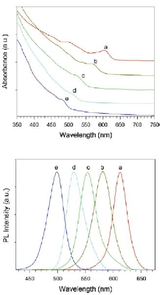
Figure 1.1 shows the PL and absorption spectra for the Cd1-xZnxSe
nanocrystals with various Zn molar fractions of 0, 0.28, 0.44, 0.55, and 0.67. In the absorption spectra, the first excitonic absorption wavelength of CdSe was quenched with the incorporation of ZnSe, while the overall shape remained similar. With the increase of the Zn fraction from 0 to 0.67, a significant blue-shift of about 110-120 nm was observed for both the first excitonic absorption onset and the band-edge luminescence peak of the nanocrystals.
Figure 1.1: Absorption (top) and PL spectra with λex=365 nm (bottom)
for the Cd1-xZnxSe nanocrystals with Zn fractions of (a) 0, (b) 0.28, (c)
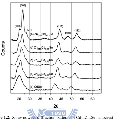
The X-ray diffraction analysis may provide us with useful information to confirm the alloy composition in the nanocrystals. As shown in Figure 1.2, the diffraction peaks of nanocrystals gradually shifted toward high 2θ regions as the Zn content was increased. This phenomenon can be realized by the fact that the replacement of Cd with Zn of smaller atomic size in alloyed nanocrystals may lead to the shrinkage in unit cell and thus the decrease in lattice spacing. As a
Figure 1.2: X-ray powder diffraction patterns of Cd1-xZnxSe nanocrystals
result, the alloyed Cd1-xZnxSe nanocrystals showed diffraction peaks at higher
2θ regions as compared to the pure CdSe.
4. Cation Exchange Reaction
Ion exchange is an exchange of ions between two electrolytes or between an electrolyte solution and a complex. Ion exchangers are either cation exchangers that exchange positively charged ions (cations) or anion exchangers that exchange negatively charged ions (anions). Cation exchange reactions have been demonstrated as useful and simple methods for preparing thin films and nanocrystals with specific composition.[29-36] The conversion reaction is kinetically prohibited at ambient conditions in the bulk due to the high activation energy required for the diffusion of ions in the solid lattice framework. Nevertheless, the activation energy decreases as particle size decreases, enabling exchange to occur within seconds for nanoparticles. Cation exchange provides a facile method for systematically varying the proportion of two chemical compositions within a single nanocrystal and studying its effect. In the present work, we successfully demonstrated that cation exchange can be used to completely convert Ag2Se nanorods to CdSe, ZnSe and Cd1-xZnxSe
alloyed nanorods. More importantly, the conversion process could be reversibly performed.
The large difference in solubility product (Ksp) is a key factor toward
direct replacement between two kinds of cations. Nanocrystals can spontaneously be converted into the other composition with smaller Ksp. For
instance, several cations including Cu+, Ag+, Sb3+, and Bi3+ have been used to replace Zn2+ in ZnS nanotubes to produce the corresponding sulfides with the preservation of the tubular shape.[28] This approach opens up a new access to design and prepare nanostructures that are difficult to be obtained through the general methods.
For the synthesis of chalcogenide semiconductors, the cation exchange has been used in most studies, whose crystal structures are determined by frameworks of the chalcogen anions (S2-, Se2-, Te2-).[30-36] The metal cations are relatively mobile in the anionic framework, making it possible to replace the cations under moderate reaction conditions. It is believed that this chemical transformation is different from the Kirkendall effect caused by the difference in diffusion flux between two chemical species.
In 2004 Alivisatos et al first reported a research about the cation exchange reaction for nanocrystal synthesis.[29] They found some interesting phenomena about the reversible transformation between CdSe and Ag2Se
Ag+ due to thermodynamically favorable regime. Note that the reverse transformation (from Ag2Se to CdSe) was thermodynamically forbidden. Such
conversion however can be achieved through a kinetically controlled approach, in which a large amount of Cd2+ and the reaction initiator (TBP, tri-butyl phosphate) were necessarily added in the growth.
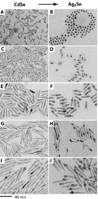
Figure 1.3 shows TEM images of the initial CdSe nanorods of different sizes and their transformed Ag2Se nanocrystals. It is apparent that thinner
nanorods (Figure 1.3A) reorganized to spherical shape during the forward reaction, which indicates that the anion sublattice was completely disrupted during the reaction (Figure 1.3B). The dependence of width and the length of initial nanorods on the morphology of the product suggested that nanorod thickness is more relevant to the shape change in the resulting product.
Figure 1.3: TEM images of CdSe nanorods of different sizes (A, C, E, G, and I) and
their transformed Ag2Se crystals (B, D, F, H, and J). As the nanorods become thicker
Besides the result reported by Alivisatos, Moon and co-workers succeeded in synthesizing various ultrathin metal telluride nanowires of MxTey
(M = Ag, Cd, Zn, Pb, and Pt).[30] The Ag2Te nanowires were converted into
CdTe, ZnTe, and PbTe using cation-exchange reactions, and the CdTe nanowires were further transformed into PtTe2 nanotubes. Figure 1.4 shows the
TEM images of the transformed metal telluride nanowires. All of the nanowires were found to preserve the initial morphology of the Ag2Te nanowires. The
crystal lattices of the nanowires obtained from HRTEM micrographs can be indexed as zinc blende for CdTe, ZnTe, and NaCl-type cubic structure for PbTe nanowires.
The governing factors for proper transformations should be considered as the follows: (1) the thermodynamic parameters that determine the transformation direction (forward and backward), (2) the kinetics of a transformation (activation barrier), (3) the effect of mechanical stress on retaining the initial shape, and (4) the mechanisms of transformations (the way of diffusion for foreign cations). When an ionic solid crystal has lower solubility than a reactant in the reaction medium, a forward reaction of ion exchange may occur. If the condition is satisfied, the kinetics can be controlled by adjusting reaction temperature to overcome the activation energy.
The chemical transformations in our study are illustrated in Scheme 1. The as-synthesized Se nanorods were first prepared and then transformed into Ag2Se nanorods. After that, the Ag2Se nanorods were converted into CdSe,
ZnSe, and Cd1-xZnxSe alloyed nanorods via cation exchange approach. We
showed that cation exchange reactions can occur completely in ionic nanocrystals at ambient pressure.
Figure 1.4: TEM and HRTEM images of (A,B) CdTe, (C,D) ZnTe, and (E,F) PbTe
Se Ag2Se CdSe
ZnSe Cd1-xZnxSe
Scheme 1: Summary of the transformations investigated in this study. The as-synthesized Se nanorods were transformed into Ag2Se nanorods by direct
incorporation of Ag+ into Se nanorods. After that, the Ag2Se nanorods were
converted into CdSe, ZnSe, and Cd1-xZnxSe alloyed nanorods through cation
II. METHOD AND ANALYSIS
1. Chemicals
All chemicals were used without further purification. 1. Selenium (IV) oxide (SeO2), 98%, Aldrich
2. Sodium borohydride (NaBH4), 96%, Fluka
3. Sodium hydroxide (NaOH), 98%, Mallinckrodt
4. Carboxymethyl cellulose (CMC), Sodium salt, 98%, Sigma 5. Silver nitrate (AgNO3), 99.9%, J.T.Baker
6. Zinc nitrate tetrahydrate (N2O6.4H2O), 98%, Riedel-deHaën
7. Cadmium nitrate hexahydrate (CdN2O6.6H2O), 98%, Fluka
8. Tri-Butyl Phosphate (TBP), 96%, Kanko Chemical
9. Polyvinylpyrrolidone (PVP), M.W. = 10000, 99%, Sigma Aldrich 10. Absolute Methanol (CH3OH), Mallinckrodt
2. Instruments and Principles
1. X-Ray Diffractometer (XRD): MAC Science, MXP18, operated at 40kV and 30mA
2. Field-Emission Scanning Electron Microscope (FESEM): JEOL, JSM-6500F, operated at 15 kV
3. Transmission Electron Microscope (TEM): Philips Tecnai, F20G2, operated at 200kV
4. UV-Visible Spectrophotometer: Hitachi, U-3900H
2.1. X-Ray Diffractometer
In XRD, a constructive interference is produced through the interaction of the incident X-ray with the sample under the regime of Bragg's Law (nλ = 2d sin θ). This law correlates the wavelength of X-ray (λ) with the diffraction angle (2θ) and the lattice spacing of crystal (d) of the sample. By scanning the sample through a wide 2θ range to collect primary diffraction peaks, one may identify the crystal structure of sample by referring to the standard reference patterns.
2.2. Scanning Electron Microscope (SEM)
The kinetic energy of accelerated electrons in SEM is dissipated as many different signals when hitting the sample surfaces. These signals mainly include secondary and backscattered electrons. Secondary and backscattered electrons are then collected and used for imaging the morphology and compositional
2.3. Transmission Electron Microscope (TEM)
In TEM, the electrons are focused with electromagnetic lenses and transmitted through the sample to image and analyze the microstructure. The electron beams are basically accelerated at several hundred kV, producing wavelength much smaller than that of light. For example, 200 kV of acceleration voltage produces electron beam with a wavelength of 0.025Å. The resolution of TEM is however limited by aberrations inherent in electromagnetic lenses, which is about 1-2 Å.
2.4. Ultraviolet–visible Spectroscopy
Absorption of incident radiation by the electrons in materials usually leads to a high frequency, i.e. low wavelength, absorption band that can be observed in the range of 200 to 800 nm. For a solution containing an absorbing substance, the absorptivity ratio at a fixed wavelength is defined as Io/I, which is logarithmically related to the concentration of solute (c) and the optical path length of sample cell (b) according to the Beer Lambert law: Absorbance (A) = log10 (Io/I) = α b c, where α is a constant named absorption coefficient.
3. Preparation of Se and Ag2Se Nanorods
3.1. Preparation of Se Nanorods:
Following a procedure developed by our group, firstly, 0.082g of SeO2
(0.74 mmole) was dissolved in 9ml of CMC solution (4.0wt%), 1ml of NaOH solution (CM = 1M) was then added with vigorous stirring at room temperature
in water-bath until the solution turned to transparent. After that, 0.03g (0.79 mmole) of NaBH4 dissolved in 1ml deionized water was added into the above
solution with the rate of 100μl/sec. The mixed solution color changed quickly from transparent to brick red, then to brown after 4 hours stirring at room temperature. This brown solution was then centrifuged at 8000 rpm for 20 min and washed with deionized water and ethanol to remove remaining ions and impurities. The washed powder (Se nanorods) was finally dried at 60oC in vacuum for 6 hours.
3.2. Preparation of Ag2Se Nanorods:
The procedure also followed the one done by our group. First of all, 0.0395g of Se (0.5 mmole) nanorods were re-dispersed in 10ml of deionized water (A solution). After that, 1.25 mmol of AgNO3 dissolved in 10 ml water
room temperature. When the color of solution turned to black after 5 hours, the experiment was stopped. The product (Ag2Se nanorods) was collected by
centrifugation at 8000 rpm for 10 min and washing with distilled water and ethanol for several times, then drying at 60oC in vacuum for 6 hours.
4. Preparation of CdSe, ZnSe and Cd1-xZnxSe Alloyed Nanorods
CdSe, and ZnSe and alloyed Cd1-xZnxSe nanorods were produced by
using the cation exchange approach from the as-synthesized Ag2Se nanorods.
0.0147g of Ag2Se nanorods (0.5×10⁻⁴ mole) were re-dispersed in 10ml of
methanol and put into a three-neck round bottom flask (solution A). Cd(NO3)2
and Zn(NO3)2 was then dissolved in 40ml of methanol contained 0.5g of PVP
(solution B). The molar ratios of Cd2+/Zn2+ used in this work are 1:0, 1:1, 1:2, 1:4, 0:1. After that, the solution B was added into the solution A at the temperature of 650C. 500μl of TBP solution was injected into the above mixed solution to proceed with the cation exchange reaction. The experiments were carried out using reflux system to make sure that the volume of the mixture solution would not change during the reaction. After the reaction time of 20 hours under vigorously stirring condition, Ag2Se was converted into CdSe
alloyed Cd1-xZnxSe) were collected by centrifugation at 8000 rpm for 5 minutes
and washed with distilled water and methanol for several times.
Scheme 2 illustrates the procedures to synthesize Se, Ag2Se, CdSe, ZnSe
0.5 mmol of Se nanorods 10 ml of H2O
Stirring at 25oC, f = 600, t = 5h
Washed with H2O, ethanol
1 mmol of AgNO3 10 ml of H2O Ag2Se (b) Synthesis of Ag2Se nanorods A solution: 0.05 mmole of Ag2Se 10 mL of methanol B solution: a mmol M(NO3)2 0.5 g PVP 40mL of methanol Adding 0.5 mL TBP At 65oC; 600rpm; t = (0.5; 1; 3; 5; 10; 15; 20) hours CdSe ZnSe Cd1-xZnxSe
(c) Synthesis of CdSe, ZnSe and alloyed Cd1-xZnxSe nanorods
Scheme 2: Illustration of the procedures to synthesize (a) Se nanorods; (b) Ag2Se nanorods; (c)
CdSe, ZnSe and Cd1-xZnxSe alloyed nanorods.
0.03g NaBH4 +1mL H2O Se 0.082g of SeO2 (0.739 mmole) 1.0 ml 1M NaOH 9mL of 4% CMC solution 0.1mL
per 5s Washed with H2O, ethanol
At 25oC; 600rpm; 4 hrs
5. Photocurrent Measurement:
A mercury-xenon lamp was used as a light source. The light intensity was calibrated with a power meter (Rapitech Enterprise Co., Ltd), but no correction was made for the reflections. The electrochemical cell was under a flowing nitrogen atmosphere (but without bubbling) to eliminate the influence of oxygen. Before measurement, the electrolyte solution was bubbled with N2
for 10 min. Photocurrent measurement were carried out in a three-armed cell with a Pt-gauze counter electrode and an Ag/AgCl electrode as a reference. An
aqueous 0.1 M Na2S solution was used as an electrolyte in all of the
measurement reported here. FTO substrates that contained various nanorods were used as working electrodes. Prior to the deposition of nanorods, the FTO-coated glass (10×10 mm2) was cleaned with ethanol for 15 min sequentially in an ultrasonic bath. The working electrode was prepared by dropping 10 μL of 5mg/mL of nanorod solution onto FTO-coated glass substrate, respectively. All measurements were carried out under ambient conditions.
6. Characterization
The morphology of the products was examined by a FESEM (Jeol, JSM-6500F) and a TEM. The crystallographic structure of the samples was investigated with XRD (MAC Science, MXP18) and HRTEM (Philips Tecnai, F20 G2) operated at 200kV. The composition of the products was obtained by the energy dispersive X-ray (EDX) Spectrometer from FESEM and TEM. The photocurrent measurement of nanorods was carried out using photoelectrochemical approach as described above. UV-visible absorption spectra were recorded using a Hitachi U-3900H at room temperature under ambient atmosphere.
III. RESULTS AND DICUSSION
1. Synthesis of Se and Ag2Se Nanorods
Se Nanorods: The FESEM image from Figure 3.1a shows the morphology of
Se nanorods prepared from the reduction of SeO2 by NaBH4 in the presence of
CMC. The dimension of the as-prepared Se nanorods was about 50-70 nm in diameter and 500-800 nm in length. The compositional information of nanorods was then studied by XRD. The corresponding XRD pattern as shown in Figure 3.1c confirms the formation of elemental Se. All the diffraction peaks in this spectrum can be indexed as the hexagonal phase of Se by referring to the reference (JCPDS, NO. 65-3404). SEM and XRD results confirm the success in synthesizing Se nanorods with considerably uniform dimensions.
Direct Introduction of Ag+ into Se Nanorods: It should be pointed out that
Ag2Se can be formed through a direct introduction of Ag+ onto Se crystals at
room temperature. The reaction in this process can be shown as follows: 3Se(s) + 6Ag+(aq) + 3H2O 2Ag2Se (s) + Ag2SeO3(aq) + 6H+[40]
A molar ratio of 2:1 of Ag+ to Se nanorods produced pure Ag2Se
nanocrystals. The EDX analysis from Figure 3.1e displays that the chemical component of the sample consists of Ag and Se. The corresponding atomic
percentages of Ag and Se are 34.46% and 16.54%, respectively. In addition, all the XRD peaks taken from Ag2Se sample are in good agreement with the
corresponding reference data of orthorhombic Ag2Se, with the lattice constants
being a = 4.33 Ao, b = 7.06 Ao, and c = 7.76 Ao (JCPDS 24-1041).
On the other hand, the SEM and TEM results in Figures 3.1b, d, f confirmed that Ag2Se nanocrystals derived from Se nanorods had rod-like
morphology. The diameter and length of Ag2Se nanorods remained unchanged
compared to those from Se nanorods.
a) b)
d)
Figure 3.1: a) FESEM image of Se nanorods; b), d) Typical FESEM and a
high-magnification FESEM image of Ag2Se nanorods derived from Se nanorods,
respectively; c) XRD patterns of Se and Ag2Se nanorods; e) SEM-EDX result for
Ag2Se nanorods; f) TEM image of a single Ag2Se nanorod. e)
c)
2. Transformation of Ag2Se Nanorods into CdSe, ZnSe and Cd1-xZnxSe
alloyed Nanorods via Cation Exchange Reactions.
2.1. Morphology of Cd1-xZnxSe Nanocrystals
After placing Ag2Se into the solvent, the reaction could be carried out in
three ways: (1) Simultaneous injection of both precursors; (2) injection of cadmium precursor followed by injection of zinc precursor; (3) injection in the reverse order. By using method (1) in our experiment, we showed that the morphology of the reaction products can be preserved as that of the initial sample. The prototypical semiconductor nanocrystal system of Ag2Se reacts
with Cd2+, Zn2+ ions to yield CdSe, and ZnSe and alloyed Cd1-xZnxSe
nanocrystals by the cation exchange reaction. Figure 3.2 shows the SEM images of a series of Cd1-xZnxSe nanorods obtained with varying amounts of zinc and
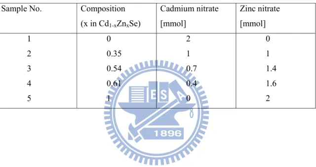
cadmium precursors, as indicated in Table 3.1. This table also contains the composition of final products determined by EDX analysis. It is very clear that the morphology of these alloyed nanorods is similar to that of initial Ag2Se. The
nanorods have diameters of 50-70 nm and lengths can be varied from 500 to 800 nm. Furthermore, we observed in all experiments that the composition of the Cd1-xZnxSe nanorods is mainly dependent on the amount of Zn2+ and Cd2+
mentioning that the Zn2+ precursor has lower reactivity, compared to Cd2+ precursor (as inferred in Table 3.1).
Table 3.1: Experimental conditions in the synthesis of Cd1-xZnxSe nanorods
Sample No. Composition (x in Cd1-xZnxSe) Cadmium nitrate [mmol] Zinc nitrate [mmol] 1 2 3 4 5 0 0.35 0.54 0.61 1 2 1 0.7 0.4 0 0 1 1.4 1.6 2
Figure 3.2: FESEM images of a) CdSe, b) Cd0.65Zn0.35Se, c) Cd0.46Zn0.54Se, d)
Cd0.39Zn0.61Se, e) ZnSe nanorods. The CdSe, ZnSe and alloyed Cd1-xZnxSe nanorods were
derived from Ag2Se nanorods via cation exchange process. The morphology of nanorods
remained unchanged after the reactions.
e)
d) c)
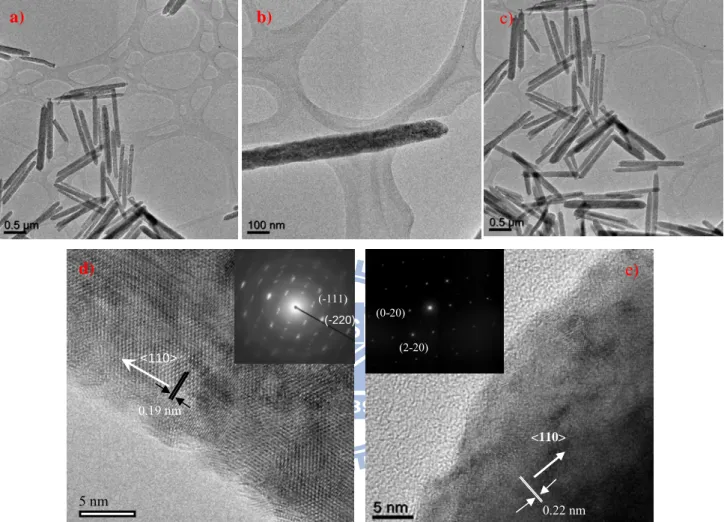
To obtain more details about structures of Cd1-xZnxSe nanorods, HRTEM
and SAED measurements were exploited. Figures 3.3 and 3.4 show the TEM images of the CdSe, ZnSe and Cd0.65Zn0.35Se nanorods. All of the nanorods
turned out to preserve the initial morphology of the Ag2Se nanorods. The
crystal lattices of the nanorods obtained from HRTEM micrographs can be indexed as wurtzite structure for both CdSe and ZnSe nanorods. HRTEM images in Figure 3.3d shows that ZnSe nanorods have interplanar spacing of 0.19 nm, which corresponds to the separation between (110) of the hexagonal crystal structure. The interplanar spacing of CdSe nanorods is 0.22 nm, indicating the separation between (110) (see Figure 3.3d). For the alloyed nanorods of Cd0.65Zn0.35Se, the interplanar spacing was observed as 0.21 nm,
also indicating the separation between (110), as shown in Figure 3.4c.
The HRTEM images in Figures 3.3d, 3.3e and 3.4c show a growth direction of [110] observed for CdSe, ZnSe and alloyed Cd0.65Zn0.35Se nanorods.
In addition, the dot-pattern of SAED (see the insets of Figures 3.3d, 3.3e and 3.4c) reveals the poly-crystallinity of ZnSe nanorods and single-crystallinity of both CdSe and alloyed Cd0.65Zn0.35Se nanorods, respectively.
Figure 3.3: a) and b) TEM images at different magnifications of ZnSe nanorods, c) TEM
image of CdSe nanorods, d) and e) HRTEM images and electron diffraction pattern (see the inset) of ZnSe and CdSe nanorods, respectively.
a) b) (-220) (-111) 5 nm d) <110> 0.19 nm <110> 0.22 nm e) (2-20) (0-20) c)
d)
Figure 3.4: a) and b) TEM images at different magnifications, c) HRTEM image and
electron diffraction pattern (see the inset), d) EDX spectrum, e) and f) Line-scan EDX profiles of Cd0.65Zn0.35Se alloyed nanorods for cadmium (red signal), zinc (green signal),
a) b) (-111) (-220) c) d) e) f) 0.21 nm
2.2. Crystallographic Structures of Cd1-xZnxSe Nanorods
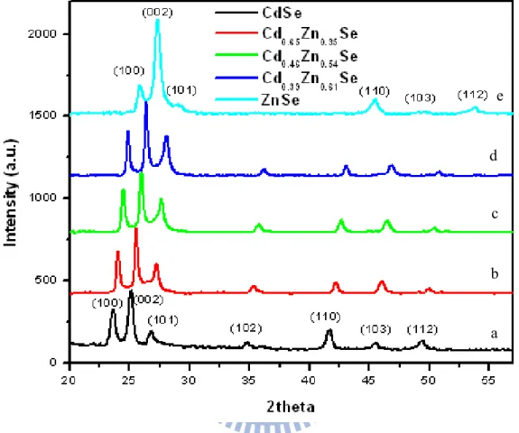
The XRD patterns of the Cd1-xZnxSe nanorods (x = 0, 0.35, 0.54, 0.61)
shown in Figure 3.5 indicate a complete cation exchange between Ag+ and Cd2+ and Zn2+. In addition, the three alloyed nanorods all exhibited the hexagonal crystal structures. The peak positions of three alloyed nanorods are in between the ones of the corresponding peaks of CdSe and ZnSe. As the composition of Zn increases, the diffraction peaks gradually shift toward higher 2θ regions, which is indicative of the transformation from the CdSe to the ZnSe lattice.
The CdSe nanorods were crystallized in the wurtzite structure with a = 4.31 Ao, c = 7.02 Ao (JCPDS 65-3415). For ZnSe case, the XRD pattern can also be indexed to the hexagonal phase (wurtzite structure). The lattice constants are a = 3.99 Ao, c = 6.27 Ao (JCPDS 89-2940).
A gradual increase in lattice spacing along the axial direction is observed with the decrease of Zn content in the nanorods (1.9 Ao for ZnSe, 2.1 Ao for Cd0.65Zn0.35Se, and 2.2 Ao for CdSe, as determined from HRTEM). This trend
confirms the formation of alloys with homogeneous distribution of ZnSe inside the CdSe matrix.
The chemical transformations were also characterized using SEM-EDX, as shown in Figure 3.6. The EDX results indicate a complete replacement of Ag+ by Cd2+ and Zn2+ ions in the cation exchange reactions. All peaks indexed
Figure 3.5: XRD patterns of CdxZn1-xSe nanorods with different Zn mole
fractions of a) 0, b) 0.35, c) 0.54, d) 0.61 and e) 1. The peaks shift toward the higher angle with the increase of zinc molar ratio from 0 to 1.
d
a c
b e
to Ag in Ag2Se nanorods disappeared after the cation exchange reaction, while
peaks assigned to Zn or Cd. The atomic percentages obtained from EDX data for CdSe were Cd = 17.3% and Se = 17.4%. For ZnSe, the atomic percentages of Zn and Se were 9.11% and 8.98%, respectively. The atomic ratios of Cd (or Zn) and Se are almost 1:1. These results are in good accordance with the XRD analyses mentioned above.
Besides, Figures 3.6 b, c, and d show the atomic percentages of Cd, Zn and Se of the three Cd1-xZnxSe alloyed nanorods. Determination of Cd:Zn ratio
yields x = 0.35, 0. 54, 0.61 with the increase of initial zinc molar ratio as shown in Table 3.1.
Furthermore, the TEM-EDX analyses shown in Figures 3.4e and 3.4f are evidences to prove that the Cd0.65Zn0.35Se nanorods are alloyed, neither
core-shell structure nor the separation of CdSe and ZnSe nanocrystals. Zinc composition distributes randomly on the rod.
Figure 3.6: EDX spectra taken from a) CdSe, b) Cd0.65Zn0.35Se, c) Cd0.46Zn0.54Se, d)
Cd0.39Zn0.61Se, e) ZnSe nanorods.
Energy (KeV)
a)
e)
c) d) b)
3. The Growth Mechanism of CdSe, ZnSe and Cd1-xZnxSe Nanorods
In order to perform the cation exchange reactions, the Ag2Se nanorods
were redispersed in methanol, and PVP was added as a stabilizer to prevent any possible agglomeration during the cation exchange process. We used nitrate salts as the precursors because they are highly soluble in methanol, the solvent used for all cation exchange reactions.
In our research, TBP also played an important role because no cation exchange was observed without TBP. TBP is believed to be able to bind to both Ag+ ions in the nanorods and Cd2+ (or Zn2+) ions in solution, forming intermediate complexes. Methanol may act as a ligand, together with TBP, to form intermediate complexes. [30]
In our experiment, the reaction took place right after the injection of TBP. The color of the resulting solutions was brown for CdSe, yellow for ZnSe, and brownish yellow for alloyed samples (see Figure 3.7). Furthermore, the
morphology of Cd1-xZnxSe nanorods kept unchanged during the cation
exchange reaction. This is confirmed by FESEM images of CdSe and ZnSe nanocrystals with different reaction times, as indicated in Figure 3.9 and Figure 3.10, respectively.
As mentioned above, the Zn2+ precursor has lower reactivity than Cd2+ precursor. This is also inferred from the change in Ag:Cd molar ratio (in synthesis of CdSe), Ag:“Cd+Zn” molar ratio (in preparation of three alloyed nanocrystals), and Ag:Zn molar ratio (for ZnSe case) when the reaction time increased from 0 to 20 hours (see Figure 3.8 and Table 3.2). In the synthesis of Cd1-xZnxSe nanorods, the reaction rate increases with the increase of cadmium
molar ratio. Besides, the reaction rate in preparation of CdSe is higher than that of ZnSe and three alloyed nanocrystals.
Cd0.39Zn0.61Se
Se Ag2Se CdSe Cd0.65Zn0.35Se Cd0.46Zn0.54Se ZnSe
Figure 3.7: Photograph of water suspensions of Se, Ag2Se, and Cd1-xZnxSe
Table 3.2: The variation in molar ratios of Ag/M (M = Cd; Zn; “Cd+Zn”) for nanorods with
the increase of the reaction times.
Ag/Cd
(CdSe) (Ag/”Cd+Zn” Cd0.65Zn0.35Se)
Ag/”Cd+Zn” (Cd0.46Zn0.54Se) Ag/”Cd+Zn” (Cd0.39Zn0.61Se) Ag/Zn (ZnSe) 0.5 1.87 7.37 5.89 7.7 5.15 1 0.97 2.09 2.37 4.35 4.29 3 0.19 0.16 0.27 1.18 1.98 5 0.09 0.12 0.12 0.21 0.94 10 0.06 0.09 0.09 0.14 0.16 20 0 0 0 0 0
Figure 3.8: Plots of the change in molar ratios of Ag/Cd, Ag/“Cd +Zn”, Ag/Zn for Reaction times
0.5
3 5
10 20
1
Figure 3.9: FESEM images of CdSe nanorods obtained by cation exchange reaction with
different reaction times from 0.5 hr to 20 hrs. Ag+ was completely replaced by Cd2+ precursors after long reaction time (about 20 hours). The morphology of nanorods remained unchanged.
Figure 3.10: FESEM images of ZnSe nanorods obtained by cation exchange reaction
with different reaction times from 0.5 hr to 20 hrs. Ag+ was completely replaced by Zn2+ precursors after long reaction time (about 20 hours). The morphology of nanorods remained unchanged. 0.5 20 5 10 3 1
It has been reported that the effectiveness in cation exchange between Ag+ and Cd2+ can be explained based on the crystal structures of Ag2Se and
CdSe. The anion sublattice in Ag2Se (orthorhombic) and CdSe (wurzite) have a
topotactic relationship. The a and b axes of Ag2Se are almost the same as the a
and c axes of CdSe (a = 4.33 Ao, b = 7.06 Ao in Ag2Se case, while the lattice
constants of CdSe are a = 4.31 Ao, c = 7.02 Ao). This results in matching of anion positions that further facilitates the in and out diffusion of Ag+ and Cd2+ through the lattice, leading to the formation of CdSe without substantial rearrangement for the Se2- sublattice. However, such topotactic relationship between the anion sublattices is not necessarily required in the present nanorod systems, since ZnSe (wurzite) does not show any topotactic relationship with either Ag2Se or CdSe.
In this context, the stronger interaction between TBP and Ag+ allows the association of Cd2+ with the anion sublattice, leading to the replacement of Ag+ by Cd2+. The reverse reaction, that is, the replacement of Cd2+ by Ag+, is spontaneous due to the large difference in solubility between Ag2Se and CdSe
(Ksp = 1×10-54 mol/L for Ag2Se and 4×10-35 mol/L for CdSe). [30]
Similarly, ZnSe has Ksp = 1.9 × 10⁻²⁷ which is higher than that of Ag2Se.
Zn2+ will not be spontaneous at room temperature, similar to the replacement of Ag+ by Cd2+. Therefore, for the synthesis Cd1-xZnxSe nanorods, we had to
employ more delicate experimental conditions (i.e., a small amount of TBP together with heating to 65 °C). The difference in solubility between CdSe and ZnSe nanocrystal is another factor that affects the result of cation exchange reaction.
4. Optical Properties of Cd1-xZnxSe Nanorods
4.1. UV-vis spectra
The room temperature UV absorption spectra of CdSe, ZnSe and Cd 1-xZnxSe nanorods in water are shown in Figure 3.11. For semiconductor
nanocrystals, the bandgap (Eg) is an important value for electron transportation.
Generally, the bandgap of semiconductor nanocrystals could be modulated by controlling the particle size, which has been widely reported. In our research, the optical absorption edge was determined by the optical absorption method [38,
39] and was derived based on the following equation:
Where α is the absorption coefficient, Eg is the bandgap, and A is a constant. The variation of (αhυ)2 with photon energy for nanorods is shown and
discussed (see inset of Figure 3.11). Bandgap values were obtained by
extrapolating the intercepts of the plots (straight lines) on the energy axis. For CdSe and ZnSe nanorods, the bandgap values are 1.75 and 2.58 eV, respectively, which match well with the literature report. The bandgap energy of Cd1-xZnxSe nanorods increases from 1.75 to 2.58 eV with the increase in Zn
concentration from 0 to 1, as shown in Table 3.3 (Eg3).
This general trend is in agreement with that obtained by Kolomiets and Ling [23] who established an empirical second-order function to describe the nonlinear evolution of the bandgap with composition in the bulk alloy.
Eg,bulk(x) = 1.74 + (0.89 – 0.75)x + 0.75x2 (1)
On the other hand, in bulk materials, the dependence of Eg on x is also
determined by equation 2, where Eig,∞ is the bulk band gap for i = ZnSe, Cd 1-xZnxSe or CdSe and b is the bowing parameter (for Cd1-xZnxSe, b = 0.35). [24]
As anticipated, the bandgap energies (Eg) of the Cd1-xZnxSe nanorods in
both cases are between those of the CdSe and ZnSe. The bandgap values based on eq. 1 and eq. 2 are Eg1 and Eg2 as revealed in Table 3.3, respectively.
Figure 3.11: Absorption spectra of Cd1-xZnxSe nanorods with different Zn/Cd molar
ratios. Bandgap values were obtained by extrapolating the linear region in plots of (αhυ)2 vs. photon energy (see inset of the figure).
Table 3.3: The bandgaps for Cd1-xZnxSe nanorods calculated by different methods I InniittiiaallCCdd22++//ZZnn22++mmoollaarrrraattiio o FFiinnaallpprroodduucctts s EEgg11[[eeVV]]((11)) EEgg22[[eeVV]]((22)) EEgg33[[eeVV]]((33)) 1 1::00 CCddSSee 11..7744 11..7744 11..7755 1 1::1 1 CCdd00..6655ZZnn00..3355SSee 11..8888 11..9966 11..9999 1 1::2 2 CCdd00..4466ZZnn00..5544SSee 22..003 3 22..1122 22..0077 1 1::4 4 CCdd00..3399ZZnn00..6611SSee 22..11 22..1199 22..1188 0 0::1 1 ZZnnSSe e 22..661 1 22..6611 22..5555
4.2. Photoconductivity
Figure 3.12a shows the photocurrent generation of Cd1-xZnxSe (x = 0,
0.35, 0.54, 0.61, 1) nanorods subjected to the on/off cycle of white light illumination. One can see that the nanorods can be reversibly switched between the low and the high conductivity state. As shown in the Figure 3.12a, a steady photocurrent was produced in CdSe, ZnSe and three Cd1-xZnxSe samples when
the irradiation was switched on and the current returned approximately to the baseline when the light was switched off.
The on/off ratio, which is defined as the current under the irradiation over the dark current, is also presented in the Figure 3.12b as a function of the illuminated time. CdSe sample shows the highest on/off ratio (approximately 7.12), the next come to Cd0.65Zn0.35Se, Cd0.46Zn0.54Se, Cd0.39Zn0.61Se samples
with the on/off ratio of about 5.74, 2.20, 2.04, respectively; and the lowest one belongs to ZnSe (~1.46). As we know, the photocurrent derives mainly from electron-hole pair excited by incident light with energy larger than the bandgap, that is, only light with enough energy is able to induce a significant increase in current. In addition, energy of a phonon in excess of the semiconductor’s bandgap (hυ > Eg) is efficiently converted to heat through electron and hole
mobility and contributing a higher conductivity. In our experiment, the wavelength of the incident light is from 400 to 800 nm. The electron-hole pair of CdSe (bandgap of 1.74 eV) can be excited by the light with the wavelength less than 710 nm. It means that most of the incident light can be used to excite and mobilize electron and hole in CdSe nanorods, resulting in higher photoconductivity as compared to alloyed Cd1-xZnxSe (x = 0.35, 0.54, 0.61, 1.74
eV <bandgap< 2.61 eV) and ZnSe (bandgap of 2.61 eV).
On the other hand, the reaction rate in CdSe case is higher than three alloys and ZnSe as mentioned above. This produced more defects in CdSe nanorods which lead to the retardation of electron-hole recombination. Therefore, the photocurrent in CdSe is higher than the alloys and ZnSe.
Figure 3.12: a) Photocurrent generation of CdSe, Cd0.65Zn0.35Se, Cd0.46Zn0.54Se, Cd0.39Zn0.61Se,
and ZnSe nanorods. b) Plots of on/off ratio as a function of time for the five nanorod samples. a)
IV. CONCLUSIONS AND PERSPECTIVE
Overall, we have demonstrated the use of cation exchange as a general and effective approach to synthesize Cd1-xZnxSe nanorods. The mechanism of
their formation were studied and discussed.
This work focused on the synthesis of Cd1-xZnxSe nanorods via the
cation exchange between the Ag+ in Ag2Se and the M2+ (M = Cd, or Zn) in
solution. All the products showed monodispersity in size, smooth surface, and rod-like shape. In these systems, the reaction of Ag2Se Cd1-xZnxSe is
intrinsically non-spontaneous at room temperature because of the large difference in solubility. As a result, the cation replacement relied on the use of TBP as a catalyst and elevation of temperature. Our results show that a topotactic relationiship between the anion sublattices was not a prerequisite for cation replacement, since ZnSe does not show any topotactic relationship with Ag2Se.
Cd1-xZnxSe nanorods were synthesized and their photoconducting
capability was demonstrated. Cd1-xZnxSe nanorods were found to be perfectly
alloyed in the entire range of Zn composition we applied. Photocurrents dramatically decreased when the zinc composition increases in alloyed samples. In on-off switching operations, the CdSe sample was found to have better
photoresponse than ZnSe and the alloyed ones. The present results demonstrate that Cd1-xZnxSe alloyed nanorods can be practically applicable to relevant
photodetectors that may cover almost full range of visible spectrum of light extending from blue to red.
As a final note, it is feasible to use cation exchange reactions to significantly expand the scope of II-VI semiconductor nanorods, for example, PbSe nanorods. We expect that this method can be extended to synthesize high-quality alloyed nanorods of other materials.
V. REFERENCES
[1]. Mathew C. Beard and Randy J. Ellingson Laser & Photonics Review 2008, 2, 377-399. [2]. Unyong Jeong, Jong-Uk Kim, and Youman Xia Nano lett. 2005, 5, 937-942.
[3]. Sasanka Deka, Alessandra Quarta, Maria Grazia Lupo, Andrea Falqui, Simona Boninelli, Cinzia Giannini, Giovanni Morello, Milena De Giorgi, Guglielmo Lanzazi, Corrado Spinella, Roberto Cingolani, Teresa Pellegrino, and Liberato Manna J. Am. Chem. Soc. 2009, 131, 2948-2958.
[4]. Ken-Tye Yong, Jun Qian, Indrajit Roy, Hoon Hi Lee, Earl J. Bergey, Kenneth M. Tramposch, Sailing He, Mark T. Swihart, Anirban Maitra, and Paras N. Prasad Nano Lett.
2007, 7, 761-765.
[5]. Ken-Tye Yong, Indrajit Roy, Haridas E. Pudavar, Earl J. Bergey, Kenneth M. Tramposch, Mark T. Swihart, and Paras N. Prasad Adv. Matter. 2008, 20, 1412-1417.
[6]. Polina O. Anikeeva, Jonathan E. Halpert, Moungi G. Bawendi, and Vladimir Bulovic
Nano Lett. 2009, 9, 2532-2536.
[7]. Chao Xu and Eric Bakker Anal. Chem. 2007, 79, 3716-3723.
[8]. Qingling Zhang, Suresh Gupta, Todd Emrick, and Thomas P. Russell J. Am. Chem. Soc.
2006, 128, 3898-3899.
[9]. Qingling Zhang, Thomas P. Russell, and Todd Emrick Chem. Mater. 2007, 19, 3712-3716.
[10]. Asit Baran Panda, Somobrata Acharya, Shlomo Efrima, and Yuval Golan Langmuir
2007, 23, 765-770.
[11]. Donghuan Qin, Hong Tao, Yun Zhao, Linfeng Lan, Keith Chan and Yong Cao
Nanotechnology 2008, 19, 355201.
[13]. LeeAnn Kim, Polina O. Anikeeva, Seth A. Coe-Sullivan, Jonathan S. Steckel, Moungi G. Bawendi, and Vladimir Bulovic Nano Lett. 2008, 8, 4513-4517.
[14]. Wenhao Liu, Hak Soo Choi, John P. Zimmer, Eiichi Tanaka, John V. Frangioni, and Moungi Bawendi J. Am. Chem. Soc. 2007, 129, 14530-14531.
[15]. Hsiao-Sheng Chen, Chih-Wei Chen, Chun-Hsiung Wang, Feng-Ching Chu, Chih-Yu Chao, Chia-Cheng Kang, Pi-Tai Chou, and Yang-Fang Chen J. Phys. Chem. C 2010, 114, 7995-7998.
[16]. Asit Baran Panda, Garry Glaspell, and M. Samy El-Shall J. Am. Chem. Soc. 2006, 128, 2790-2791.
[17]. Qing Peng, Yajie Dong, Zhaoxiang Deng, and Yadong Li Inorg. Chem. 2002, 41, 5249-5254.
[18]. Bonil Koo and Brian A. Korgel Nano Lett. 2008, 8, 2490-2496.
[19]. Dmitri V. Talapin, Elena V. Shevchenko, Christopher B. Murray, Andreas Kornowski, Stephan Forster, and Horst Weller J. Am. Chem. Soc. 2004, 126, 12984-12988.
[20]. Dmitri V. Talapin, James H. Nelson, Elena V. Shevchenko, Shaul Aloni, Bryce Sadtler, and A. Paul Alivisatos Nano Lett. 2007, 7, 2951-2959.
[21]. Nishshanka N. Hewa-Kasakarage, Maria Kirsanova, Alexander Nemchinov, Nickolas Schmall, Patrick Z. El-Khoury, Alexander N. Tarnovsky, and Mikhail Zamkov J. Am. Chem.
Soc. 2009, 131, 1328-1334.
[22]. Jian-Ping Ge, Sheng Xu, Jing Zhuang, Xun Wang, Qing Peng, and Ya-Dong Li Inorg.
Chem. 2006, 45, 4922-4927.
[23]. Myriam Protière and Peter Reiss Small 2007, 3, 399-403.
[24]. Steven A. Santangelo, Eric A. Hinds, Vladimir A. Vlaskin, Paul l. Archer, and Daniel R. Gamelin J. Am. Chem. Soc. 2007, 129, 3973-3978.
[25]. Xinhua Zhong, Zhihua Zhang, Shuhua Liu, Mingyong Han, and Wolfgang Knoll J.
Phys. Chem. B 2004, 108, 15552-15559.
[26]. Fang-Chen Liu, Tian-Lu Cheng, Chien-Chih Shen, Wei-Lung Tseng, and Michael Y. Chiang Langmuir 2008, 24, 2162-2167.
[27]. Xinhua Zhong, Mingyong-Han, Zhili Dong, Timothy J. White, and Wolfgang Knoll J.
Am. Chem. Soc. 2003, 125, 8589-8594.
[28]. LarissaDloczik; Rolf Könenkamp Nano Lett. 2003, 3, 651.
[29]. Dong Hee Son, Steven M. Hughes, Yadong Yin, A. Paul Alivisatos Sciences 2004, 306, 1009-1012.
[30]. Geon Dae Moon, Sungwook Ko, Younan Xia, and Unyong Jeong ACS NANO 2010, XXX, 000-000.
[31]. Unyong Jeong, Pedro H. C. Camargo, Young Hwan Lee, and Younam Xia J. Matter.
Chem. 2006, 16, 3893-3897.
[32]. Yungwon Park, Jaimei Zheng, Young-wook Jun, and A. Paul Alivisatos J. Am. Chem.
Soc. 2009, 131, 13943-13945.
[33]. Wei Zhu, Wenzhong Wang, and Jianlin Shi J. Phys. Chem. B 2006, 110, 9785-9790. [34]. Richard D. Robinson, Bryce Sadtler, Denis O. Demchenko, Can K. Erdonmez, Lin-Wang Lin-Wang, A. Paul Alivisatos Science 2007, 317, 355-358.
[35]. Joseph M. Luther, Haimei Zheng, Bryce Sadtler, and A. Paul Alivisatos J. Am. Chem.
Soc. 2009, 131, 16851-16857.
[36]. Unyoung Jeong, Younan Xia, Yadong Yin Chemical Physics Letters 2005, 416, 246-250.
[37]. Xinhua Zhong,Mingyong Han, Zhili Dong,Timothy J. White,and Wolfgang Knoll J.
Am. Chem. Soc. 2003, 125, 8589.
[38]. Y. S. Wang, P. John Thomas, and P. O’Brien J. Phys. Chem. B 2006.
[39]. Saliha Ilican, Muhsin Zor, Yasemin Caglar, Mujdat Caglar Optica Applicata 2006, XXXVI, 29-37.
[40]. Byron Gates, Yiying Wu, Yadong Yin, Peidong Yang, and Youman Xia J. Am. Chem.