348 /
CLEO
2001/ WEDNESDAY AFTERNOON
cw15 5 3 0 pm
Uitrahlgh bandwidth MSM travellngwave photodetectors
Jin-Wei Shi, Kian-Giap Gan,* Yi-Jen Chiu,* Chi- Kuang Sun,** Yin-Jay Yang,’ John. E Bowers:
Graduate Institute of Electro-Optical Engineering, National Taiwan University, Taipei, TAIWAN, R.O.C.; *Department ofElech-ical and Computer Engineering, University of California, Santa Barbara, CA 93106, USA; **Graduate Institute of Electro-Optical Engineering and Department of Electrical Engineering, National Taiwan University, Taipei, T N W m , R.O.C.; E-mail: [email protected]; +Department of Electrical Engineering, National Taiwan University, Taipei, T A I W m , R.O.C.; *Department of Electrical and Computer Engineering, University of California, Santa Barbara, CA 93106, USA
Traveling-wave photodetector (TWPD) at - tracts attentions due to its high bandwidth-effi- ciency product by replacing the traditional R-C bandwidth limitation by velocity mismatch be- tween optical/electrical waves in a waveguide structure. A bandwidth-efficiency product of 76 GHz (with 180 GHz bandwidth) at 800 nm wavelength was demonstrated with GaAs-based p-i-n TWPD structures.’ Recently a record band- width of 560GHz was achieved in the same wave- length regime using low-temperature-grown (LTG) GaAs as the photo-absorption la ye^ of a p-i-n TWPD, utilizing the sub-picosecond carri- er trapping time of the LTG-GaAs at the expense of internal quantum efficiency. Even though high bandwidth performance was already demon- strated, due to the slow microwave propagation mode in a p-i-n structure, further bandwidth im- provement was limited by the velocity mismatch bandwidth. In this paper we demonstrate a new type of ultra-high speed photodetector: MSM TWPD. By utilizing LTG-GaAs as the absorption layer, this device structure provides quasi-TEM microwave mode with a velocity close to or even higher than the optical velocity with an extreme- ly wide velocity matched bandwidth. MSM TWPD structure has a better bandwidth perfor- mance than p-i-n TWPD owing to its lower mi-
S. I. GaAs substrate
I
Y
“Self9lign”Photbabsorptianregion
Flared out CPW mglon for m‘oowave probe (b)
C W 5 Fig. 1. (a) Device cross sectional dia- gram and (b) top view.
crowave loss, higher microwave velocity, and bet- ter impedance matching between the electrical transmission line of TWPDs and external electric load. With a preliminary device fabrication using self-aligned structures, the measured impulse re- sponse exhibits 0.8 ps pulsewidth with a corre- sponding 3 dB bandwidth over 570 GHz even under high power excitation. Even wider band- width performance was obtained for low power excitation. These side-pumped MSM TWPDs also have a better efficiency (>5%) compared with LTG-GaAs based MSM vertically-illuminat- ed photodetectors.’ Without complex isolation process or E-beam lithography, this novel device is easily fabricated and offers a better way than p- i-n TWPD or MSM VPD to be integrated as TWPD array for high power THz emitters.
The cross section and top view of the demon- strated MSM TWF’D device are shown in Fig. 1. 3pm-thick &.,Ga&s layer is designed for opti- cal isolation. Qm-thick Alo.3,G~.a& and 500nm-thick LTG-GaAs are for waveguiding and photo;absorption purposes. Utilizing only semi- insulating LTG-GaAs and high resistive undoped semiconductor layers, this device has much lower microwave loss, higher microwave velocity, and better impedance matching between TWPDs and external electrical load or transmission line than p-i-n based TWPDs, implying that MSM-TWPD has a wider bandwidth than p-i-n based TWPD especially for long-length device with high satu- ration current. Three metal strips act as CPW to collect the photo-generated microwave signal. The center strip is naturally separated with ground planes by the depth and under-cut pro- file of etched ridge-mesa, and 200
-
300 nm dis- tance between metal strips was easily achieved without complex E-beam lithography. This nar- row-gap CPW can not only increase the respon- sivity of TWPD due to short carrier transport time but reduce microwave radiation loss when it operates near THz regime.-0.2
-
,.
, , ,.
,.
-2 0 2 4 6 Time (psec) 3dB Electrical Bgndwidth 0.0.
’ . ’ . ” ’ .’
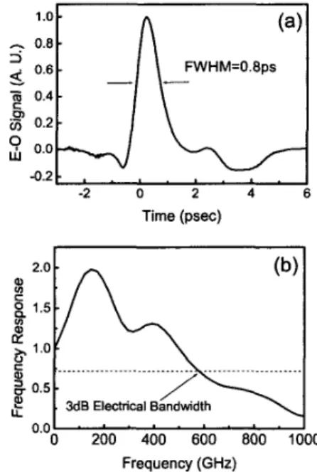
0 200 400 600 800 1000 Frequency (GHz)CWI5 Fig. 2. (a) E O response of a MSM TWPD under 800 nm excitation and (b) its cor- responding Fourier transform.
Figure 2 shows an example of the device im- pulse response under 2.3 mW average power ex- citation with an 80 MHz 150fs Tisapphire laser at 800 nm. 0.8 ps pulsewidth with a transformed 3dB bandwidth of 570 GHz (fig. 2b) was ob- tained. With lower power excitation, pulsewidth will drop down to the order of 0.5 ps with an even higher 3 dB bandwidth. The total quantum efficiency is -5% under high bias. More bias-de- pendent and annealing-temperature-dependent performances will be discussed in our presenta- tion.
Reference
K.S. Giboney, M.J.W. Rodwell, and J.E. Bow- ers, “Traveling-Wave Photodetector Design and Measurements,” IEEE Journal Of Selected Topics In Quantum Electronics, 2, 622-629
(1996).
Y.J. Chiu, S.B. Fleischer, and J.E. Bowers, “High-speed Low-Temperature-Grown GaAs p-i-n Traveling-Wave Photodetector,”
IEEE Photon. Technol. Lett. 10, 1012-1014
(1998).
S.Y Chou and M.Y. Liu, “Nanoscale Tera- Hertz Metal-Semiconductor-Metal Pho- todetectors,” IEEE Journal of Quantum Elec- tronics, 28,2358-2368 (1992).
CW16 6:OO pm
Ultrafast ail+ptlcal switching using a frequency shift accompanied by cross- phase modulation in a semiconductor optical amplifier
Shigeru Nakamura, Yoshiyasu Ueno, Kazuhito Tajima, System Devices and Fundamental Research, NEC Corporation, 34 Miyukigaoka, Tsukuba, Ibaraki 305-8501, Japan; E-mail: s-
All-optical switches are quite attractive for opti- cal demultiplexing and for other various optical signal processing in future optical-time-division- multiplexing (OTDM) networks. Optical demul- tiplexers will likely require switching operation for more than 100-Gbps signals at a repetition rate of 1 0 4 0 GHz with low control-light power.’ A promising approach for such applications is a transient cross-phase modulation (T-WM) all- optical switch?’ which features not only ultrafast switching with low control-light power but also a quite simple configuration. The simple configu- ration leads to many advantages such as com- pactness, stability, and polarization-insensitivity. In this report, we present ultrafast (correspon- ding to 168-Gbps demultiplexing) and high-rep- etition (10 GHz) operations of the T-XPM all-
optical switch with a control-pulse energy of less than 1 pJ. These operations have been achieved by using a semiconductor optical amplifier (SOA) as a nonlinear waveguide and setting the control pulse duration shorter than the signal pulse duration.
The T-XF’M all-optical switch is composed of a semiconductor nonlinear waveguide and a filter (Fig. l(a)). In the nonlinear waveguide, an ultra- short control pulse excites a carrier density change and thus causes a nonlinear phase shift for the signal light. This nonlinear phase shift rapidly rises nearly within the control-pulse du- ration and then slowly relaxes. Ultrafast switch- ing with the T-XPM switch is made possible by