國 立 交 通 大 學
電子工程學系 電子研究所碩士班
碩 士 論 文
高介電氧化層
MOSFET元件之低漏電
電荷幫浦量測技術
A Low Leakage Charge Pumping Measurement Technique
for High-K MOSFET’s
研 究 生 :朱益輝
指導教授 :莊紹勳 博士
高介電氧化層
MOSFET 元件之低漏電電荷幫浦量測技術
A Low Leakage Charge Pumping Measurement Technique
for High-K MOSFET’s
研
究 生 : 朱益輝 Student : Yi - Huei Ju
指導教授
: 莊紹勳 博士 Advisor : Dr. Steve S. Chung
國立交通大學
電子工程學系
電子研究所碩士班
碩士論文
A Thesis
Submitted to Department of Electronics Engineering & Institute of
Electronics College of Electrical Engineering and Computer Science
National Chiao Tung University
in Partial Fulfillment of the Requirements
for the Degree of
Master of Science
in
Electronics Engineering
July 2005
Hsinchu, Taiwan, Republic of China.
高介電氧化層
MOSFET 元件之低漏電電荷幫浦量測技術
學生:朱益輝
指導教授:莊紹勳
博士
國立交通大學
電子工程學系﹙研究所﹚碩士班
摘
要
當元件氧化層持續微縮時,以二氧化矽為基底做為 CMOS 元件的氧化層會有其物 理極限上的限制,故以高介電係數材料當作元件氧化層是一個重要的課題。然而,除了 移動率降低與臨界電壓漂移的問題之外,因為高介電係數氧化層本身具有相當多的缺 陷,造成電荷快速的捕捉與釋放,而形成臨界電壓的不穩定亦是另一個可靠性的問題。 所以,發展一套簡單、快速且適用於高介電係數氧化層結構的方法去分析電荷捕捉的特 性顯得相當重要。而不僅僅是使用高介電係數氧化層,利用環狀離子佈植去改善短通道 效應也是不可或缺的。然而,不同的環狀離子佈植也會造成元件不同的退化情形。
本論文將著重在利用差頻電荷幫浦法(IFCP, Incremental Frequency Charge Pumping)
去分析90 奈米 N 型高介電係數氧化層 MOSFET 元件。我們結合 IFCP 方法和陷阱到矽 基板傳導帶的穿遂時間常數來得知缺陷在高介電係數氧化層的位置。一開始,透過這個 量測方法,我們可以發現缺陷的產生和閘極偏壓的條件有相當密切的關係。在基板注入 時,它對高介電係數氧化層造成的傷害較大,而介面傷害程度較大是發生在閘極注入。 在本文的後半,對於N 通道 MOSFET 元件,我們透過高溫正偏壓的操作下來加速 元件的衰退現象。由於高溫正偏壓不穩定性的測試對於使用環狀離子植入製程所成的邊 緣傷害並不明顯,所以,我們利用高溫時的熱載子效應測試,來有效的觀測閘極邊緣傷
害的程度。藉由實驗的結果,我們可以發現藉由較大質量環狀離子佈植,它臨界電壓的 不穩性或介面陷阱的產生會來的比較少。
A Low Leakage Charge Pumping Measurement Technique
for High-K MOSFET’s
Student:Yi - Huei Ju
Advisors:Dr. Steve S. Chung
Department of Electrical Engineering & Institute of Electronics
National Chiao Tung University
ABSTRACT
The aggressive scaling of CMOS devices has driven SiO2-based gate dielectrics to its
physical limits, as a result, high-K materials as a gate stack has attracted a lot of interests. However, apart from mobility degradation and threshold voltage (VT) shifts, VT instability
caused by trapping and detrapping of pre-existing defects is another reliability concern. Therefore, it becomes important to develop a simple and fast method to quantitatively characterize charge traps in high-k dielectrics. Not only high K gate stack is needed, but also halo implant process with short channel effect control is inevitable. However, various degradations of the devices with different halo implant species incurred.
This thesis has been focused on utilizing IFCP(Incremental Frequency Charge Pumping) method for the measurement of high gate dielectrics 90nm nMOSFET’s. By combining IFCP method and trap-to-band tunneling time constant, the calculation of trap position in the HfSiON has been implemented. By using this technique, it was found that the correlation
damage in HfSiON during substrate injection. While, during gate injection, it induces more traps in the Si/IL (interfacial layer) interface.
We have also studied the n-MOSFET device degradation through PBTI(Positive Bias Temperature Instability) stress in the later half of this thesis. Since PBTI is not a sensitive test to distinguish the effect of different halo implant species from the gate edge, PBTI-like stress has been employed to provide an understanding of the degradation at the gate edge. From the experimental results, we can find that the VT instability and interface trap generation are
誌 謝
在兩年碩士研究生涯中,首先要向我的指導教授莊紹勳老師表達深摯的謝意。尤其 是老師對於事物的嚴謹態度,使我在處理事情的態度上有所成長。除此之外,他對於學 生的默默關懷,我必須在此表達感謝之意。 兩年的實驗室生活是精采豐富的,但同時也充滿了艱辛與汗水。在此同時我也要感 謝學長們的指導與提攜,他們使我建立了研究應有的態度,尤其是紹弘學長、前泰學長 與旻政學長,當我在學業上遇到挫折時,你們總是不斷的給予支持與鼓勵,使我能在研 究上無後顧之憂。而在日常生活上,感謝那些和我一起嚐遍酸甜苦辣的同學,包括又仁、 靖泓、冠德與書人,還有汪研究群的同學們:晉輝、小馬、智維、晉豪,希望未來的日 子裡,大家除了可以共患難外亦可共享福。總歸一句,感念所有的夥伴,因為你們的陪 伴,使我兩年研究生活豐富,即使艱辛,仍充滿歡笑。 最後要感謝是我的家人和女友雅君,你們是我精神上最大的支柱,所有的壓力在回 家和你們閒聊中得以解脫。沒有你們默默的支持和關愛,我無法堅持到最後。 謹將這份榮耀獻給培養我多年的父母親。Contents
Chinese Abstract
iEnglish Abstract
iiiAcknowledgements
vContents
viFigure Captions
viiChapter 1 Introduction
11.1 The Motivation of This Work 1
1.2 Organization of This Thesis 2
Chapter 2 Device Fabrication and Experimental Measurements
32.1 Introduction
3
2.2 Device Fabrication 4 2.3 The Low Leakage IFCP Technique 4 2.3.1 Basic Experimental Setup 4 2.3.2 Experimental Setup of Charge Pumping Measurement 7 2.3.3 Principle of the Low Leakage IFCP Method 7
2.3.4 Principle of the IFCP Measurement for High–K Dielectrics 11 2.4 Extraction of the Traps in High-K Dielectrics 15 2.5 Summary 17
Chapter 3 Investigation of the Properties in HfSiON Film
18 3.1 Introduction 183.2 Device Fabrication 18
3.3 The Analysis of Reliability in nMOSFET Devices 19
3.3.1 Theoretical Calculations 19
3.3.2 IFCP for High-K Devices 20 3.4 Results and Discussion 22 3.5 Summary 37
Chapter 4
The Analysis of PBTI and PBTI-like Reliabilities in Different Halo Implant High–K N-MOSFET’s 38 4.1 Introduction 38 4.2 Results and Discussion 38 4.2.1 The Devices Under Test 39 4.2.2 PBTI Stress 394.2.3 PBTI-like Stress 43
4.3 Summary 48
Chapter 5 Summary and Conclusion
49Figure Captions
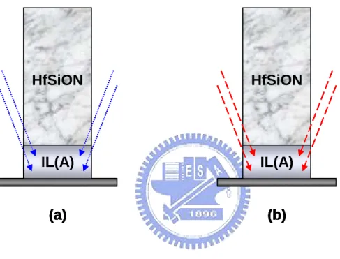
Fig. 2.1 Schematic illustration of device with different Halo implant species. (a) using light atomic mass unit implant in Halo(1);(b) using heavy atomic mass unit implant in Halo(2).
Fig. 2.2 The experiment setup for the current-voltage measurement. An automatic controlled characterization system is set up based on the PC controlled instrument environment.
Fig. 2.3 Basic experimental setup for the charge pumping measurement.
Fig. 2.4 The schematic of charge pumping (CP) for (a) nMOSFET measurement. (b) pMOSFET measurement. Induced leakage current(IG) occurs when tox< 20A.
Fig. 2.5 Measured ICP at two different frequencies. The low leakage IFCP method is
achieved by subtracting ICP current at two successive frequencies.
Fig. 2.6 Measured ICP at two frequencies. We can find the inconsistency of the results
using IFCP method.
Fig. 2.7 This figure shows ICP,200 KHz correct = 2.ICP,100 KHz correct, and we can apply IFCP
to high-K devices.
Fig. 2.8 The recombined charge per cycle (Qcp) for the high-k device. The charge
pumping current is seen to increase for lower frequencies indicating that the charge pumping current is the sum of an interface trap component and a bulk trap in high-k dielectric.
Fig. 3.1 Bandgap diagram of the high-k dielectric in the excess electron state, showing trap-to-band tunneling (T-B).
Fig. 3.2 Comparison of the trap density in HfSiON for two different halo implant species, where halo(2) causes more damage in HfSiON close to the interfacial layer.
Fig. 3.3 The measurement flow used to monitor the trap generation. Before each set of charge-pumping measurements, a short non-stressing negative voltage is applied.
Fig. 3.4 The correlation between the shift of threshold voltage and time dependence. It seems not to cause the obvious damage using the discharging voltage.
Fig. 3.5 Comparison of the trap density in HfSiON in halo(1) during negative gate voltage stress.
Fig. 3.6 Comparison of the trap density in HfSiON in halo(2) during negative gate voltage stress.
Fig. 3.7 Comparison of the trap density in HfSiON in halo(1) during positive gate voltage stress.
Fig. 3.8 Comparison of the trap density in HfSiON in halo(2) during positive gate voltage stress.
Fig. 3.9 Comparison of the interface trap density in halo(1) for two different stress voltages. The interface trap generation is faster, during negative voltage stress. Fig. 3.10 Comparison of the interface trap density in halo(2) for two different stress
voltages. The interface trap generation is faster, during negative voltage stress. Fig. 3.11 Comparison of the bulk trap density in halo(1) for two different stress voltages.
The bulk trap in HfSiON generation is faster, during positive voltage stress. Fig. 3.12 Comparison of the bulk trap density in halo(2) for two different stress voltages.
The bulk trap in HfSiON generation is faster, during positive voltage stress. Fig. 3.13 Schematic band diagram of a SiO2/HfSiON gate stack for substrate injection.
High energetic electrons arrive at the anode and generate electron-hole pair. Fig. 3.14 Schematic band diagram of a SiO2/HfSiON gate stack for gate injection. High
energetic electrons arrive at the anode and hole injection leads to interface degradation.
Fig. 4.1 Comparison of the trap density in HfSiON in halo(1) pre-PBTI stress and post-PBTI stress.
Fig. 4.2 Comparison of the trap density in HfSiON in halo(2) pre-PBTI stress and post-PBTI stress.
Fig. 4.3 Comparison of the interface trap density in different halo implant species during pre-PBTI stress and post-PBTI stress.
Fig. 4.4 Comparison of the trap density in HfSiON in halo(1) pre-PBTI-like stress and post-PBTI-like stress.
Fig. 4.5 Comparison of the trap density in HfSiON in halo(2) pre-PBTI-like stress and post-PBTI-like stress.
Fig. 4.6 The threshold voltage shift for different halo implant species.
Fig. 4.7 Comparison of the interface trap density in different halo implant species during pre-PBTI-like stress and post-PBTI-like stress.
Chapter 1
Introduction
1.1 The Motivation of This Work
The physical limitation of the conventional silicon dioxide as gate dielectric has reached the point where films thickness is only a few atomic layers thick. With the scaling of CMOS devices, the gate leakage current will increase exponentially with the reducing gate oxide thickness. High dielectric constant (high-k) materials implemented in CMOS technologies as gate dielectrics will eventually be needed to relieve the rapid gate current increase associated with the aggressive oxide thickness scaling. The increasing dielectric constant allows for increased physical thickness at similar driving capability. Among the many potential high-k materials under investigation, hafnium-based dielectrics has been a good candidate and be a good replacement for SiO2 gate insulator [1], [2].
The most promising candidate with sufficient high k-value is currently HfO2. Recently,
HfSiON has been successfully integrated into CMOS as gate dielectrics for low power applications, with good reliability, comparable mobility (as SiO2) and significantly reduced
gate leakage [3]. With the demands for high-K gate dielectrics to replace conventional SiO2/SiOxNy, it turns out to be inevitable for continuous device scaling, integrating high-K
materials and polysilicon gate electrode into deep sub-micron CMOS technology without significant device degradation has become one of the most challenging task [4], [5]. Apart from mobility degradation and threshold voltage (Vt) shifts, Vt instability is caused by
develop a simple and fast method to quantitatively characterize charge traps in high-k dielectrics.
Also, during measurement, we need to overcome the induced leakage current using any of the above methods. In [8], it has been demonstrated successfully an IFCP (Incremental Frequency Charge Pumping) method for the interface characterization.
In this thesis, traps at various location of a stacked dielectric have been characterized by charge-pumping (CP) technique combined with multiple frequency measurement. The excellent correlation of all types of traps to process conditions makes this method very promising for the applications in high-k dielectrics development.
1.2 Organization of this thesis
This thesis has been divided into five chapters. Chapter 2 describes the devices used in this work and experimental setup. The low leakage IFCP method for high-K dielectrics will be used to determine interface traps and the traps in high-K dielectrics. At the same time, the evaluation will be described. In Chapter 3, we will use the method of Chapter 2 to discuss stress polarity dependent Constant Voltage Stress (CVS) on NMOSFETs with a polysilicon gate and HfSiON gate dielectric. In Chapter 4, we also use the same method to investigate the effect of halo implants species under PBTI(Positive Bias Temperature Instability) and PBTI-like stress conditions. Finally, a summary and conclusion will be given in Chapter 5.
Chapter 2
Device Fabrication and Experimental Measurements
2.1 Introduction
To reduce the high gate leakage, current major efforts are focused on replacing SiO2 and
SiON with high-k gate dielectrics. If a material with a dielectric constant larger than 3.9 of SiO2 is used, the same equivalent oxide thickness ( EOT ) can be reached with a physically
thicker layer. This ultimately leads to a reduction of the gate leakage current and allows further scaling of the gate oxide. The most promising candidate with sufficient high k-value is currently HfO2, but unfortunately there is an interaction with the poly-Si gate, leading to
Fermi level pinning, and large defect densities as well as VT instabilities are reported [9].
Only when metal gate electrodes are used, most of the unwanted effects disappear and the poly-Si depletion can be eliminated. From the integration point of view, poly-Si electrodes are still preferred and be used to speed up the introducing of high-k dielectrics. Hf-silicates (HfSiON) most likely will be the first to be introduced in integrated CMOS. Hf-silicates proved compatibility with poly-Si gate processing while maintaining good electrical characteristics. HfSiON can only be introduced if reliability is guaranteed [10]. However, the direct tunneling leakage is still large under EOT scaling down to below 16Å.
In order to analyze the reliability property of NMOSFET’s in thin HfSiON in the following chapters, we use a simple charge pumping method. As a result, the measurement setup and basic theory used are listed here. This chapter is divided into several sections. In the first section, the devices used in this study are examined. Then, the experimental analysis
methods used in thesis will be introduced, including the low leakage IFCP method for high-k dielectrics.
2.2 Device Fabrication
MOS devices were fabricated based on advanced 90nm CMOS technology. The high K film deposited by ALD ( atomic layer deposition ) is HfSiON, while HfSiON films received post-deposition NH3 annealing. A given interfacial layer film was formed on a Si(100)
wafer prior to high K film deposition. Interfacial layer film used in this work is nitrogen-incorporated SiO2. All wafers received HF cleaning prior to growing interfacial layer
film. Halo(1) and halo(2) are two different implant species for light AMU and heavy AMU, respectively. Fig. 2.1 shows the device fabrication process.
2.3 The Low Leakage IFCP Technique
2.3.1 Basic Experimental Setup
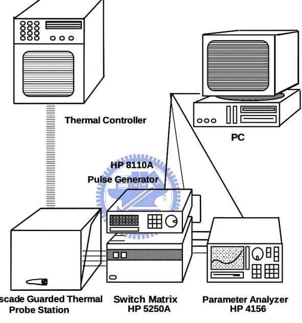
The experimental setup for the I-V measurement of MOS device is illustrated in Fig. 2.2. Based on the PC controlled instrument environment, the complicated and long-term characterization procedures for analyzing the intrinsic and degradation behavior in MOSFET’s can be easily achieved. As shown in Fig. 2.2, the characterization equipment, including the semiconductor parameter analyzer (HP4156c), the dual channel pulse generator (HP8110A), low leakage switch mainframe (HP E5250A), the cascade guarded thermal probe station and thermal controller, provides an adequate capability for measuring the device I-V characteristics.
Light Atomic Mass Unit
Heavy Atomic Mass Unit
IL(A)
(a)
HfSiON
IL(A)
(b)
HfSiON
Light Atomic Mass Unit
Heavy Atomic Mass Unit
Light Atomic Mass Unit
Heavy Atomic Mass Unit
IL(A)
(a)
HfSiON
IL(A)
(b)
HfSiON
IL(A)
(a)
HfSiON
IL(A)
(a)
IL(A)
(a)
HfSiON
IL(A)
(b)
HfSiON
IL(A)
(b)
IL(A)
(b)
HfSiON
Fig. 2.1 Schematic illustration of device with different Halo implant species. (a) using light atomic mass unit implant in Halo(1);(b) using heavy atomic mass unit implant in Halo(2).
HP 8110A Pulse Generator
Cascade Guarded Thermal Probe Station Switch Matrix HP 5250A Parameter Analyzer HP 4156 PC Thermal Controller
Fig. 2.2 The experiment setup for the current- voltage measurement. An automatic
controlled characterization system is set up based on the PC controlled instrument environment.
HP 8110A Pulse Generator
Cascade Guarded Thermal Probe Station Switch Matrix HP 5250A Parameter Analyzer HP 4156 PC Thermal Controller HP 8110A Pulse Generator
Cascade Guarded Thermal Probe Station Switch Matrix HP 5250A Parameter Analyzer HP 4156 PC Thermal Controller
Fig. 2.2 The experiment setup for the current- voltage measurement. An automatic
controlled characterization system is set up based on the PC controlled instrument environment.
2.3.2 Experimental Setup of Charge Pumping Measurement
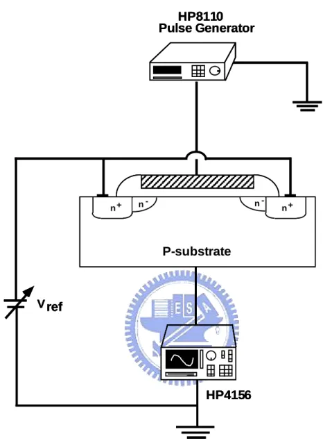
The basic setup of charge pumping measurement is shown in Fig. 2.3. The source, drain and bulk electrodes of tested devices are grounded. A 1MHz square pulse waveform provided by HP8110A with fixed base level (Vgl) is applied to NMOS gate, or with fixed top level (Vgh)
is applied to PMOS gate. We keep Vgl at –1.0V while increase Vgh from –1.0V to 1.0V by
step 0.1V, or keep Vgh at 1.0V while decrease Vgl from 1.0V to –1.0V by step –0.1V.
With a smaller voltage step, we get a higher profiling resolution. The parameter analyzer HP4156C is used to measure the charge pumping current (ICP).
2.3.3 Principle of the Low Leakage IFCP Method
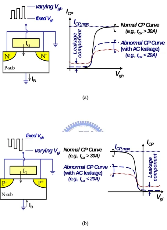
Figures 2.4 (a) and (b) show the schematic of a low leakage IFCP measurement for CMOS developed by [8]. With both S/D grounded and by applying a gate pulse with a fixed base level (Vgl) and a varying high level voltage (Vgh) for NMOS, the channel will operate between
accumulation and inversion. This gives rise to the charge pumping current ICP (=IB) measured
from the bulk. However, leakage current IG is unavoidable, as we see from Fig. 2.4 (a), the
leakage of ICP is very small when tox >30Å. However, it was revealed in Fig. 2.5 that the
leakage current increases, curves (1) and curves (2), for tested sample. From the measured ICP
at two frequencies, ƒ1 and ƒ 2, can be expressed as :
ICP,ƒ 1 with-leakage= ICP,ƒ 1 correct + ICP,leakage@ƒ1 (2.1)
and
Pulse GeneratorHP8110
n + n - n - n +
P-substrate
Vref
HP4156
Fig. 2.3 Basic experimental setup for the charge pumping measurement. Pulse GeneratorHP8110 n + n - n - n + P-substrate Vref HP4156 Pulse GeneratorHP8110 n + n - n - n + P-substrate Vref HP4156
Fig. 2.4 The schematic of charge pumping (CP) for
(a) nMOSFET measurement. (b) pMOSFET measurement. Induced leakage current(IG) occurs when tox< 20A.
Normal CP Curve Abnormal CP Curve (with AC leakage) (e.g., tox> 30A) (e.g., tox< 20A)
V
glI
CPI
CP,max Le ak ag e co mpo n en t varying Vgl fixed Vgh IBP
+P
+ N-sub IG Normal CP Curve Abnormal CP Curve (with AC leakage) (e.g., tox> 30A) (e.g., tox< 20A)V
ghI
CPI
CP,max Leakage component varying Vgh fixed Vgl IBN
+N
+ P-sub IG (a) (b)Fig. 2.4 The schematic of charge pumping (CP) for
(a) nMOSFET measurement. (b) pMOSFET measurement. Induced leakage current(IG) occurs when tox< 20A.
Normal CP Curve Abnormal CP Curve (with AC leakage) (e.g., tox> 30A) (e.g., tox< 20A)
V
glI
CPI
CP,max Le ak ag e co mpo n en t varying Vgl fixed Vgh IBP
+P
+ N-sub IG Normal CP Curve Abnormal CP Curve (with AC leakage) (e.g., tox> 30A) (e.g., tox< 20A)V
ghI
CPI
CP,max Leakage component varying Vgh fixed Vgl IBN
+N
+ P-sub IG (a) (b)
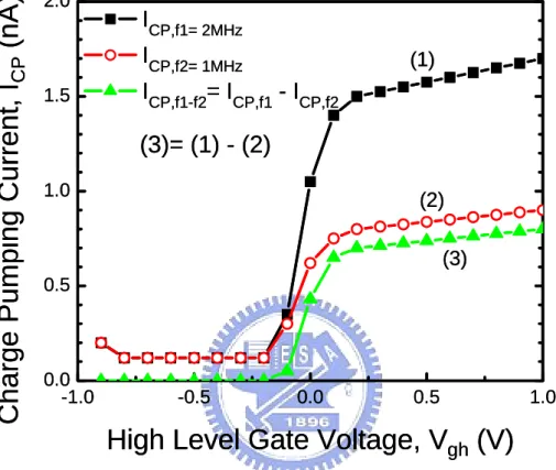
Fig. 2.5 Measurement ICP at two different frequencies. The low leakage
IFCP method is achieved by substracting ICPat two successive frequencies -1.0 -0.5 0.0 0.5 1.0 0.0 0.5 1.0 1.5 2.0
(3)= (1) - (2)
Charge Pumping Current
, I
CP(n
A)
High Level Gate Voltage, V
gh(V)
I
CP,f1= 2MHzI
CP,f2= 1MHzI
CP,f1-f2= I
CP,f1- I
CP,f2 (1) (2) (3)Fig. 2.5 Measurement ICP at two different frequencies. The low leakage
IFCP method is achieved by substracting ICPat two successive frequencies -1.0 -0.5 0.0 0.5 1.0 0.0 0.5 1.0 1.5 2.0
(3)= (1) - (2)
Charge Pumping Current
, I
CP(n
A)
High Level Gate Voltage, V
gh(V)
I
CP,f1= 2MHzI
CP,f2= 1MHzI
CP,f1-f2= I
CP,f1- I
CP,f2 (1) (2) (3)When the frequency is sufficiently high, the leakage components in these two frequencies are almost the same (ICP,leakage@ƒ1 ≈ ICP, leakage@ƒ2 ). We then take the difference of
ICP (∆ICP, ƒ 1- ƒ 2) between two frequencies. From equations (2.1) and (2.2), the difference of
these two CP curves gives :
∆ICP,ƒ 1-ƒ 2 = ICP,ƒ 1 with-leakage - ICP,ƒ 2 with-leakage. (2.3)
Since the correct CP curve is directly proportional to the frequency, it will be equal to the difference of two CP curves. Therefore, in the IFCP method, the correct CP curve at frequency (ƒ1- ƒ2) can be given by
ICP,ƒ 1-ƒ 2 = ∆ICP,ƒ 1-ƒ 2. (2.4)
For example, ICP(2MHz) - ICP(1MHz) is regarded as the ICP at their difference frequency,
1MHz. The correct result is shown in curve (3).
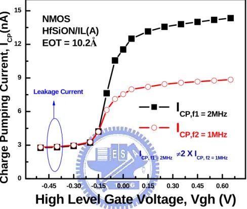
2.3.4 Principle of the IFCP Measurement for High–K Dielectrics
We mentioned that low leakage IFCP measurement can reduce the leakage component and extract interface state density accurately. Unfortunately this excellent method can not be applied to high K devices due to fast oxide traps. When a low frequency is applied to the gate, the ICP includes two component which are ICP,Nit and ICP,Not. On the other hand, a high
phenomenon has already been described by R. Degraeve and A. Kerber [11]. Fig. 2.6 shows the charge pumping measurement at 1MHz and 2MHZ. We could find unreasonable results since ICP has two components at low frequency, if we applied the IFCP measurement to high
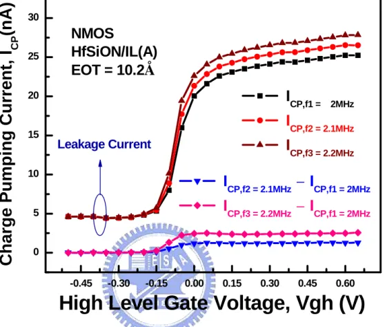
K device. In the meanwhile, we also find that high frequency CP measurement is more sensitive in gauging the interface state density. Using this characteristic, we improve IFCP for high K device. Eqs. (2.5), (2.6), and (2.7) show the ICP that measured for high K device, i.e.,
ICP,ƒ1=2MHz with-leakage= ICP,ƒ 1=2MHz,Nit + ICP,ƒ 1=2MHz,Not + ICP,leakage@ƒ 1 (2.5)
and
ICP,ƒ 2=2.1MHz with-leakage= ICP,ƒ2=2.1MHz,Nit + ICP,ƒ 2=2.1MHz,Not + ICP,leakage@ƒ2 (2.6)
and
ICP,ƒ 3=2.2MHz with-leakage= ICP,ƒ 3=2.2MHz,Nit + ICP,ƒ 3=2.2MHz,Not + ICP,leakage@ƒ 3. (2.7)
Since the DC leakage currents are the same, we will take out leakage current by IFCP method. IFCP for high K can expressed as :
ICP,100KHzcorrect= ICP,ƒ 2=2.1MHz,Nit - ICP,ƒ 1=2MHz,Nit (2.8)
and
ICP,200 KHz correct= ICP,ƒ 3=2.2MHz,Nit - ICP,ƒ 1=2MHz,Nit. (2.9)
If the correct CP curve is directly proportional to the frequency, it will be equal to the difference of two CP curves. Furthermore, we show evidences to prove that IFCP can be applied to high K devices, shown in Eq. (2.10) and Fig. 2.7
-0.45 -0.30 -0.15 0.00 0.15 0.30 0.45 0.60 0 3 6 9 12 15 ICP, f1 = 2MHz ≠2 X ICP, f2 = 1MHz
I
CP,f1 = 2MHzI
CP,f2 = 1MHzCharge P
u
mpi
ng Curre
n
t,
I
CP(n
A)
High Level Gate Voltage, Vgh (V)
Leakage Current
NMOS
HfSiON/IL(A) EOT = 10.2Å
Fig. 2.6 Measured ICP at two frequencies. We can find the inconsistency
-0.45 -0.30 -0.15 0.00 0.15 0.30 0.45 0.60 0 5 10 15 20 25 30
NMOS
HfSiON/IL(A)
EOT = 10.2Å
I
CP,f2 = 2.1MHz-
I
CP,f1 = 2MHzI
CP,f3 = 2.2MHz-
I
CP,f1 = 2MHzI
CP,f1 = 0.2MHzI
CP,f2 = 2.1MHzI
CP,f3 = 2.2MHzCharge Pumpi
ng Current
, I
CP(nA)
High Level Gate Voltage, Vgh (V)
Leakage CurrentFig. 2.7 This figure shows ICP,200 KHz correct = 2.ICP,100 KHz correct, and we can apply IFCP to
As aforementioned, we can monitor the charge pumping current by observing the interface trap density for high K devices.
2.4 Extraction of the Traps in High-K Dielectrics
The technique of charge pumping is frequently used in the study of interface traps by applying a square wave to the gate of the device and measuring the resulting current through the source and drain. The interface traps charge and discharge with a charge pumping current (ICP) directly proportional to frequency f; however, the charge recombined per cycle (QCP =
ICP/f remains the same irrespective of the measurement frequency [12]. In a device, with traps
located spatially near Si/IL (interfacial layer) interface, is held in inversion for a period of time longer than the tunneling time constant, then communication may occur between the interface traps and traps in the high-K film. This results in an additional current component and gives rise to an increase of the charge recombined per cycle. In this work, devices fabricated with the HfSiON film are characterized by a high concentration of traps in the high-k film with a well-defined trapping distance, corresponding to the interfacial layer.
Fig. 2.8 shows that at low frequency, nMOS exhibits significantly higher Nt. Such
charge trapping in nMOS not only reduces the amount of free carriers in the channel but also serves as additional coulomb scattering centers to lower the electron mobility. Nt of nMOS
can be divided into two parts based on its dependence on frequency: one is frequency independent part named as interface traps (Nit), which locates at Si/IL interface next to
channel with very short time constant. Another is frequency dependent part, which is referred to as oxide traps (Not) of the HfSiON layer. In this thesis, we will separate the influence of the
Fig. 2.8 The recombined charge per cycle (Qcp) for the high-k device. The charge pumping
current is seen to increase for lower frequencies indicating that the charge pumping current is the sum of an interface trap component and a bulk trap in high-k dielectric..
2000000 4000000 6000000 8 9 10 11 12 13 14 15
Charge Recombi
ned per Cycle(10
-1 0
)
Frequency (Hz)
nMOSFET Halo(1) W/L= 10/0.09µm EOT=10.2Åcharge-pumping experiment. Since, by varying the charge-pumping frequency we can sense different fractions of the trap density. Therefore, using the above skill and the time constant of the electron trap-to-band tunneling detrapping process, it will help us to obtain the trap density in the HfSiON away from the interfacial layer.
2.5 Summary
In this chapter, experimental analysis methods have been described. In the latter discussions, we will use these experimental techniques to discuss the traps in the gate dielectrics and interface trap in Si/IL (interfacial layer) for nMOSFET under CVS (constant voltage stress). By using the IFCP method and the method of separating Nit and Not, the
Chapter 3
Investigation of the Properties in HfSiON Film
3.1 Introduction
Device scaling is a driving force of semiconductor industry in productivity and performance as predicted by Moor’s law. Nano-scale MOSFET transistor and MOS capacitor have reached their fundamental limits and the introduction of new gate dielectric materials has been surveyed and investigated for a continued scaling. As a trade-off for very short channel device length, ultra-thin and high quality gate oxide is strongly needed. Among them, high-K materials as a gate stack has attracted great interest. Recently, HfSiON has been successfully integrated into CMOS as gate dielectrics for low power applications, with good reliability and comparable mobility.
Although, high-k dielectrics increase the physical thickness, the direct tunneling leakage still exists with EOT (equivalent oxide thickness) scaling down to below 16Å. Therefore, the leakage current will induce measurement error for ultra-thin gate dielectrics CMOS devices. To investigate the properties of HfSiON correctly, we need to eliminate the leakage current during the measurement by the IFCP method. The traps in the HfSiON and interface will be evaluated.
The devices used in this work were fabricated using 0.09µm CMOS technology. Test samples is nMOSFET which has halo implant with SiO2 and the effective oxide thickness is
10.2Å. Furthermore, both of the high-k films is HfSiON with different halo implant species including light AMU and heavy AMU.
3.3 The Analysis of Reliability in nMOSFET Devices
3.3.1 Theoretical calculations
Figure 2.8 shows that an abrupt increase of the charge recombined per cycle is observed for frequency less than 5MHz. This is due to traps in HfSiON within a tunneling distance of the interface which was filled and empty along with the interface traps resulting in an increase in the charge recombined per cycle. As the frequency is lowered the applied gate voltage drives the device into inversion for a longer time, it allows trap-to-band tunneling to take place where not only the interface traps are filled but also the traps within a tunneling distance appropriate for that particular frequency.
The time constant of the electron trap-to-band tunneling detrapping process has been derived by Lundkvist et al.[13]with a WKB analysis, and is given by
) exp( ) exp( ) exp( ) , ( * 0 X x x x T T B oxe ot ne T B ne B T
φ
τ
α
α
τ
α
τ
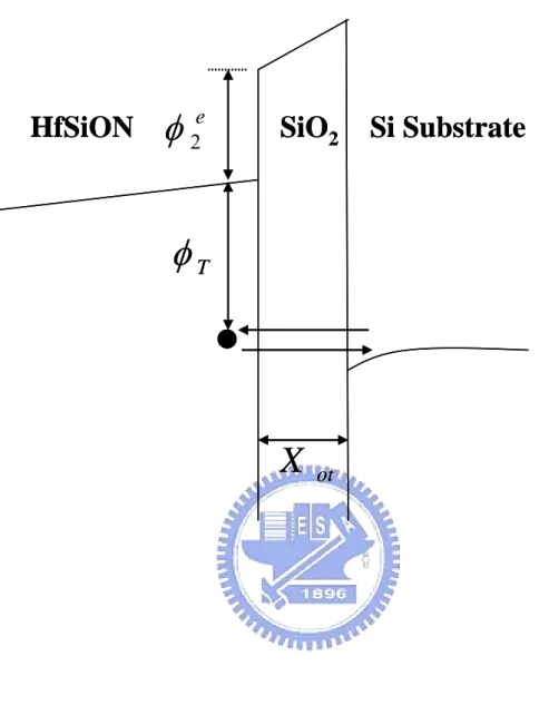
− = − = − (3.1)where τT−Bo is a time constant for the traps studied [14], φT is the normalized trap energy
(V) (qφT is the trap energy (eV) referenced to the conduction band edge in the HfSiON. And, q is the absolute electron charge), Xot is the thickness of the interfacial layer, and x is the
tunneling distance inside the HfSiON, as shown in Fig 3.1. The coefficients e ox
α and e n α depends weakly on the electric field across the gate dielectrics. Under a weak internal electric field, they can be approximated as
) ( 2 2 ) ( * 2 , T e e ox T e ox φ m qφ φ α = + h (3.2) and T e n T e n φ m qφ α * , 2 2 ) ( h = . (3.3)
Here, h is the reduced Plank’s constant, * ,e
ox
m and m*n,e are the electron effective mass in
the oxide and nitride respectively, e
2
φ is the normalized conduction band offset (V) of the interfacial layer and the HfSiON as shown in Fig 3.1.
3.3.2 IFCP for High-K Devices
Charge-pumping is commonly used to measure the interface trap density, but based on previous section, it can also sense traps in HfSiON defect band. By varying the charge-pumping frequency, we can sense the different component of the trap density in HfSiON away from the interfacial layer.
The Icp current has three components, Nit, Not and leakage current, respectively. From
IFCP, we can eliminate the contribution of Nit and leakage current and the remaining part is
Fig. 3.1 Bandgap diagram of the high-k dielectric in the excess electron state, showing trap-to-band tunneling (T-B). e 2
φ
Tφ
otX
Si Substrate
HfSiON
φ
2eSiO
2 Tφ
otX
Si Substrate
HfSiON
SiO
21. First, we can obtain the Icp,100K from the subtraction Icp,5M from Icp,5.1M. At these
high frequencies, the Icp,100K can only be treated as the contribution of Nit.
2. Then, we choose two frequencies which correspond to the particular position. Using the above method, we could eliminate the contribution of Nit from the two
frequencies we choose.
3. Later, we take the difference of ICP’S at two close frequencies. By this way, it can
remove the DC leakage. The remainder is only the Not component.
4. Because it does not sense the same trap in HfSiON every time, so that the low frequency Icp is unstable. In order to solve this problem, we examined five times
and tale an average of these values.
3.4 Results and Discussion
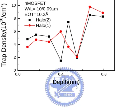
The trap density of vertical direction in HfSiON by halo implants with different halo implant species is plotted in Fig. 3.2. It seems that the sample with halo(2) causes more damage in the HfSiON near the interfacial layer, while does not affect the remaining part of the high-k layer. The higher trap density near the interfacial layer in halo(2) may be caused by using heavier atoms of the implant. And, it seems that it does not have influence on the location of the films away from the interfacial layer.
In order to measure the trap generation during electrical stress, a constant voltage stress is interrupted at regular intervals and a non-stressing voltage is applied before evaluation with charge-pumping. A schematic diagram of the stress and measurement sequence is shown in
Fig. 3.2 Comparison of the trap density in HfSiON for two different halo implant species, where halo(2) causes more damage in HfSiON close to the interfacial layer.
0.0 0.4 0.8 0 2 4 6 8 10
Trap Density(10
10/c
m
2)
Depth(nm)
nMOSFET W/L= 10/0.09µm EOT=10.2Å Halo(2) Halo(1)Fig. 3.3 The measurement flow used to monitor the trap generation. Before each set of charge-pumping measurements, a short non-stressing negative voltage is applied.
Fresh Device
Charge Pumping
V
amp= 1 V
V
base= - 1 V
at Various Frequency
Stress @ V
G
>0
Discharge
- 1 V for 15 sec
Fresh Device
Charge Pumping
V
amp= 1 V
V
base= - 1 V
at Various Frequency
Stress @ V
G
>0
Discharge
- 1 V for 15 sec
HfSiON. And, it does not cause damage to the device as can be seen in Fig. 3.4. The increase of the bulk HfSiON trap density with different halo implant species during positive and negative gate voltage stress is plotted in Fig. 3.5, Fig. 3.6, Fig. 3.7, and Fig. 3.8. It can be found that, for VG < 0V, the variation of bulk trap is not obvious. On the contrary, we can see
clearly the increase of bulk trap during the positive gate voltage stress.
In order to explain this phenomenon further, we see the trap generation versus stress time at fixed certain depth clearly. Fig. 3.9, Fig. 3.10, Fig. 3.11, and Fig. 3.12 show the increase of the interface trap density and the bulk trap density versus time during positive and negative gate voltage stresses. We can see that the interface trap generation is larger during gate injection than that for substrate injection. While, the bulk trap generation is just the reverse compared to the interface trap generation in that the bulk trap generation is larger during positive gate voltage stress. We can utilize Fig. 3.13 and Fig. 3.14 to explain the phenomenon. During substrate injection, the electron will be attracted toward the gate dielectric. Then, it generates electron-hole pairs at the anode. The generated hot hole moves toward cathode and causes the injury on the gate dielectric. So, for positive stress polarity, trap creation occurs mainly in high-k dielectric. During negative gate voltage stress, trap generation is located at the interface. In case of gate injection, high energetic electrons arrive at the anode and hole injection leads to interface degradation. Because of the large difference in k-value between SiO2 and HfSiON, the voltage drop occurs mainly in the interfacial layer and electrons can
enter the anode with energy with respect to the Si conduction band. This is why it produces more interface traps during negative gate voltage stress.
Fig. 3.4 The correlation between the shift of threshold voltage and time dependence. It seems not to cause the obvious damage using the discharging voltage.
10 100 1000 0.00018 0.00020 0.00022 0.00024 0.00026 0.00028 0.00030
Delta Thresholde Voltage,
∆
V
thstress time(s)
nMOSFET halo(1) W/L= 10/0.09µm EOT=10.2Å stress@V G=-1VFig. 3.5 Comparison of the trap density in HfSiON in halo(1) during negative gate voltage stress. 0.0 0.2 0.4 0.6 0.8 0 5 10 15 20
T
rap
s Den
s
ity(
10
10/cm
2)
Depth (nm)
nMOSFET Halo(1) W/L= 10/0.09µm EOT=10.2Å Stress@V G=-2V fresh stressedFig. 3.6 Comparison of the trap density in HfSiON in halo(2) during negative gate voltage stress. 0 2 4 6 8 1 2 3 4 5 6 7 8 9 10
Traps Densi
ty(10
10/cm
2)
Depth (nm)
nMOSFET Halo(2) W/L= 10/0.09µm EOT=10.2Å Stress@V G=-2V 1000s fresh stressedFig. 3.7 Comparison of the trap density in HfSiON in halo(1) during positive gate voltage stress. 0.0 0.2 0.4 0.6 0.8 0 5 10 15 20 25 30
Traps Density(10
10/cm
2)
Detpth (nm)
nMOSFET Halo(1) W/L=10/0.09µm EOT=10.2Å stress@VG=+2V 1000s fresh stressedFig. 3.8 Comparison of the trap density in HfSiON in halo(2) during positive gate voltage stress. 0.0 0.2 0.4 0.6 0.8 2 4 6 8 10 12 14
Tarp Density(10
10/c
m
2)
Depth, (nm)
nMOSFET Halo(2) W/L=10/0.09µm EOT=10.2Å fresh stress@V G=2V 1000sFig. 3.9 Comparison of the interface trap density in halo(1) for two different stress voltages. The interface trap generation is faster, during negative voltage stress.
10 100 1000 2.7 2.8 2.9 3.0 3.1 3.2 3.3
Interface Trap, D
it(10
11/cm
2)
stress time (S)
nMOSFET Halo(1) W/L= 10/0.09µm EOT=10.2Å stress@V G=2V 1000s stress@-2VgFig. 3.10 Comparison of the interface trap density in halo(2) for two different stress voltages. The interface trap generation is faster, during negative voltage stress.
10 100 1000 2.6 2.7 2.8 2.9 3.0 3.1 3.2 3.3
Interface Trap, D
it(10
11/cm
2)
stress time (S)
nMOSFET Halo(2) W/L= 10/0.09µm EOT=10.2Å stress@V G=+2V stress@VG=-2VFig. 3.11 Comparison of the bulk trap density in halo(1) for two different stress voltages. The bulk trap in HfSiON generation is faster, during positive voltage stress.
10 100 1000 2.0 2.2 2.4 2.6 2.8 3.0 3.2 3.4 3.6
Trap Density
(10
10/cm
2)
stress time (S)
nMOSFET Halo(1) W/L= 10/0.09µm EOT=10.2Å stress@VG=+2V stress@VG=-2VFig. 3.12 Comparison of the bulk trap density in halo(2) for two different stress voltages. The bulk trap in HfSiON generation is faster, during positive voltage stress.
10 100 1000 2.0 2.5 3.0 3.5 4.0 4.5
Trap Density
(10
10/cm
2)
stress time (S)
nMOSFET Halo(2) W/L= 10/0.09µm EOT=10.2Å stress@VG=+2V stress@VG=-2VFig. 3.13 Schematic band diagram of a SiO2/HfSiON gate stack for substrate injection. High
energetic electrons arrive at the anode and generate electron-hole pair.
n
+pol
HfSiON
Si
2
S
n
+pol
HfSiON
Si
2
S
Fig. 3.14 Schematic band diagram of a SiO2/HfSiON gate stack for gate injection. High
energetic electrons arrive at the anode and hole injection leads to interface degradation.
n
+pol
HfSiON
Si
2S
substrat
n
+pol
HfSiON
Si
2S
substrat
3.5 Summary
In this chapter, we combine IFCP method and trap-to-band tunneling time constant to calculate the trap position in the HfSiON. The IFCP method improves traditional charge pumping measurement by eliminating direct tunneling leakage current in ultra-thin gate dielectric films for MOS devices, and helps us to calculate more accurate traps in the HfSiON. On the other hand, we successfully separate Nit and Qot with IFCP method for high-k
dielectrics.
According to the experimental results, we found the correlation between trap generation and stress polarity dependence. During substrate injection, it will cause more oxide traps in the high-k dielectrics. While during gate injection, it induces more damage in the Si/IL interface. Based on the above analysis, the developed method is useful for the understanding of the properties and reliability in the high-k dielectric devices.
Chapter 4
The Analysis of PBTI and PBTI-like Reliabilities in
Different Halo Implant High–K N-MOSFET’s
4.1 Introduction
In order to improve the electrical properties and reliability of ultra-thin gate dielectric films for MOS devices, extensive studies have been made. The PBTI effect arises at high temperatures under the influence of small positive voltages on the gate of n-channel transistors. The effect seen is a shift in the threshold of the transistor to more positive gate voltages, and a decrease in the ID,sat curve due to an increase in the amount of trap charge in
the HfSiON, as well as an increase in interface state densities.
In chapter 3, we have already used the IFCP method to investigate the properties under constant voltage stress (CVS). In this chapter, we will also use the method to investigate the device reliability under PBTI and PBTI-like stress conditions. Through the PBTI reliability testing, we found that PBTI was not sufficient to distinguish halo implant with different atomic mass unit. Because PBTI testing is a sensitive measurement for monitoring a uniformly distributed high K film quality, in regarding to the gate edge damage caused by halo implant, it can not provide a better way to study the device reliability. As a consequence, in order to clearly identify the degradation at the gate edge, we use the IFCP measurement to observe Not and Nit by employing PBTI-like stress.
4.2.1 The Devices Under Test
The devices used in this work were fabricated using 90nm CMOS technology. In this section, we use the devices with gate dielectric thickness (EOT= 10.2Å) to investigate the PBTI and PBTI-like stress with different halo implant species with halo(1) and halo(2), respectively.
4.2.2 PBTI Stress
First, we stress the nMOSFET with VG= 2V at 100oC for 1000 seconds. After finishing
the stress, we use the method described in the previous chapter to calculate traps in the HfSiON and interface trap, as described in chapter 2. We can draw the distribution of traps along the direction of gate dielectric thickness. As revealed in Fig. 4.1 and Fig. 4.2, we observe the PBTI effect for different halo implant species. Fig. 4.3 shows the variation of interface traps during PBTI stress. The difference between halo(1) and halo(2) is the edge damage. It seems that it has not being able to characterize these two samples with different halo implant species clearly. Because through the PBTI reliability testing, it was not sensitive enough to distinguish halo implant with different atomic mass unit. PBTI testing is a sensitive measurement for monitoring overall high K film quality, as regards gate edge damage caused by halo implant is not the best examination. In order to investigate the degradation of gate edge more clearly, we use the IFCP measurement to observe Not and Nit after employing
Fig. 4.1 Comparison of the trap density in HfSiON in halo(1) pre-PBTI stress and post-PBTI stress. 0.0 0.2 0.4 0.6 0.8 4 6 8 10 12 14 16 18
Oxide
T
rap
, N
ot(10
10/cm
2)
Depth (nm)
nMOSFET(Halo1) W/L= 10/0.09µm EOT=10.2Å stress@VG=2V 1000s Temperature=100 °C fresh stressFig. 4.2 Comparison of the trap density in HfSiON in halo(2) pre-PBTI stress and post-PBTI stress. 0.0 0.2 0.4 0.6 0.8 4 6 8 10 12 14 16 18
Trap Densi
ty(10
10/cm
2)
Depth (nm)
nMOSFET Halo(2) W/L= 10/0.09µm EOT=10.2Å stress@V G=2V 1000s Temperature=100 °C fresh stressFig. 4.3 Comparison of the interface trap density in different halo implant species pre-PBTI stress and post-PBTI stress.
0.0 0.5 1.0 1.5 2.0 2.5 3.0 3.5 4.0 4.5 5.0 5.5 6.0 Halo(2) Stress Halo(1) Stress Halo(2) Fresh In terfa ce Trap D ensi ty, D it (1 0 11 /c m 2 ) Halo(1) Fresh nMOSFET W/L= 10/0.09µm EOT=10.2Å stress@VG=2V 1000s Temperature=100 °C
4.2.3 PBTI-like Stress
In this section, the nMOSFET was stressed under PBTI-like condition (VG= VD= 2V,
Temp= 100oC) for 1000 seconds. We may expect that the damage of PBTI-like includes the combined PBTI effect and HC effect. From IFCP results for two different samples, we can observe the amount of Nit and Not under PBTI-like stress condition. Since high K film has
many traps, electrons will be trapped in the high-k gate dielectric near the source and drain edge, during hot carrier stress. This phenomenon has already been reported recently [15]. From this depiction, we find that the amounts of traps generated in halo(1) are less than that of halo(2). According to Fig. 4.4 and Fig. 4.5, we confirm halo(2) with heavy AMU implant form significantly more trap in the high-k film. For longer-channel length nMOSFET, local degradation does not greatly affect device characteristics. In contrast, for shorter-channel devices, this local degradation affects the device characteristics significantly. This can also be revealed from Fig. 4.6. Since more oxide traps cause more serious delta threshold voltage shift, for longer-channel nMOSFET, local degradation does not greatly affect device characteristics. In contrast, for shorter-channel devices, this local degradation affects the device characteristics significantly. Therefore, the increase of interface trap comparison between halo(1) implant and halo(2) implant can reflect the damage in the interface close to the gate edge after PBTI-like stress condition as shown in Fig. 4.7. The less amount of traps seen in HfSiON with halo(1) implant compared to halo(2) implant explains more serious damage at gate edge for halo(1) implant sample. In brief, the interface trap generation correlates closely with the traps in high-k gate dielectric near the source and drain side. When a large number of oxide traps are generated near gate edge border, the damage at gate edge will be lowered.
Fig. 4.4 Comparison of the trap density in HfSiON in halo(1) pre-PBTI-like stress and post-PBTI-like stress. 0.0 0.2 0.4 0.6 0.8 2 4 6 8 10 12 14 16 18 20
Trap Dens
ity
(10
10/cm
2)
Depth (nm)
nMOSFET halo(1) W/L= 10/0.09µm EOT=10.2Å stress@VG=VD=2V 1000s Temperature=100 °C fresh stressedFig. 4.5 Comparison of the trap density in HfSiON in halo(2) pre-PBTI-like stress and post-PBTI-like stress. 0.0 0.2 0.4 0.6 0.8 2 4 6 8 10 12 14 16
Trap Density(10
10/cm
2)
Depth (nm)
nMOSFET halo(2) W/L= 10/0.09µm EOT=10.2Å stress@V G=VD=2V 1000s Temperature=100 °C fresh StressedFig. 4.6 The threshold voltage shift for different halo implant species. 10 100 1000 0.03 0.04 0.05 0.06 0.07 0.08 0.09 0.10
Delt
a
Threshol
de Vol
tage,
∆
V
thstress time(S)
nMOSFET W/L= 10/0.09µm EOT=10.2Å stress@VG=VD=2V 1000s Temperature=100 °C Halo(2) Halo(1)Fig. 4.7 Comparison of the interface trap density in different halo implant species during pre-PBTI-like stress and post-PBTI-like stress.
0.0 0.5 1.0 1.5 2.0 2.5 3.0 3.5 4.0 4.5 5.0 5.5 6.0 Halo(2) Stress Halo(1) Stress Halo(2) Fresh In ter face Tr ap Densit y , D it (1 0 11 /c m 2 ) Halo(1) Fresh nMOSFET W/L= 10/0.09µm EOT=10.2Å stress@VG=VD=2V 1000s Temperature=100 °C
4.3
Summary
In this chapter, we use the IFCP method and trap-to-band tunneling time constant to obtain the traps in the HfSiON and Nit after various stress conditions. We have investigated
the degradation of PBTI and PBTI-like condition from the observation of Nit and Not. We can
find that the amounts of oxide traps in halo(1) implant are less than that in halo(2) implant, it results in a higher effective stress field that causes worse damage to the interface near the drain extension region under PBTI-like stress condition. On the other hand, for nMOS, the decrease of the impact ionization rate is due to negative charge trapping which reduces the gate dielectric electric field.
Chapter 5
Summary and Conclusion
Alternative gate oxide material is a trend on the scaling of oxide thickness, but the direct tunneling leakage is still large with EOT scaled down to below 16Å. We utilize IFCP method and trap-to-band tunneling time constant to obtain the distribution of Qot in the HfSiON. The
IFCP method has been validated to remove the tunneling leakage current during measurement such that Nit and Qot can be separated.
In this thesis, the test samples with different halo implant species, Halo(1) and Halo(2), representing Halo implant species with light AMU and heavy AMU have been used for the study. The stress polarity and time dependence of CVS effect were performed. Subsequently, the halo implant species dependence of PBTI and PBTI-like effect were evaluated.
Based on the experimental results, we have identified the correlation between trap generate and stress polarity dependence. During substrate injection, it will cause more oxide traps in the high-k dielectrics. While, during gate injection, it induces much more damage in the Si/IL interface. Furthermore, our study shows that the amounts of traps in Halo(1) are lower than in HfSiON, resulting in higher effective stress field that causes worse damage to the interface near the gate edge under PBTI-like stress condition. On the other hand, for nMOS, the decrease of the impact ionization rate is due to negative charge trapping which reduces the gate dielectric electric field. Therefore, for reliability test, the content of nitrogen in gate oxide will become increasingly important in future nanoscale CMOS devices before using high-k dielectrics.
References
[1] S. S. Chung, S. M Cheng, G. H. Lee, and J. C. Guo, “, Direct Observation of the Lateral Nonuniform Channel Doping Profile in Submicron MOSFET's from an Anomalous Charge Pumping Measurement Results,” in Symposium on VLSI Tech., pp. 103-104, 1995.
[2] S. S. Chung and J. -J. Yang, “A New Approach for Characterizing Structure-Dependent Hot-Carrier Effects in Drain-Engineered MOSFET's,” IEEE
Trans. Electron Devices, Vol. 46, No. 7, pp. 1371-1377, 1999.
[3] H. C.-H. Wang, S.-J. Chen, M.-F. Wang, P.-Y. Tsai, C.-W. Tsai, T.-W. Wang, S.M. Ting, T.-H. Hou, P.-S. Lim, H.-J. Lin, Y. Jin, H.-J. Tao, S.-C. Chen, C.H. Diaz, M.-S. Liang, and C. Hu, “Low power device technology with SiGe channel, HfSiON, and poly-Si gate,” in IEDM Tech. Dig., pp. 161-164, 2004
[4] J. Cai and C. -T. Sah, “Interfacial Electronic Traps in Surface Controlled Transistors,”
IEEE Trans. Electron Devices, Vol. 47, No.3, pp. 576-583, 2000.
[5] S. S. Chung, S. J. Chen, and D. K. Lo, “Interface Characterization Methodology for nano-CMOS Reliability-Process and Device Reliability Monitors,” Proceedings of the
10th IPFA, July 7-11, Singapore, pp. 127-133, 2003.
[6] S. Zafar, A. Callegari, E. Gusev, and M. V. Fischetti, “Charge trapping related threshold voltage instabilities in high permittivity gate dielectric stacks,” J. Appl. Phys, Vol. 93, No.11, pp. 9298–9303, 2003.
[7] A. Kerber, E. Cartier, L. Pantisano, M. Rosmeulen, R. Degraeve, T. Kauerauf, G. Groeseneken, H. E. Maes, and U. Schwalke, “Characterization of the VT-instability in
SiO2/HfO2 gate dielectrics,” Proc. IEEE International Reliability Phys. Symp. (IRPS),
[8] S. S. Chung, S. J. Chen, C. K. Yang, S. M. Cheng, S. H Lin, Y. C. Sheng, H. S. Lin, K. T. Hung, D. Y. Wu, T. R. Yew, S. C. Chien, F. T. Liou, and F. Wen, “A Novel and Direct Determination of the Interface Traps in Sub-100 nm CMOS Devices with Direct Tunneling Regime (12/spl sim/16 A) Gate Oxide,” in Symposium on VLSI
Tech., pp. 11-13, 2002.
[9] A. Kerber, E. Cartier, L. Pantisano, R. Degraeve, T. Kauerauf, Y. Kim, A. Hou, G. Groeseneken, H. E. Meas, and U. Schwalke, “Origin of the Threshold Voltage Instability in SiO2/HfO2 Dual Layer Gate Dielectrics,” IEEE Elec. Dev. Lett., Vol. 24,
No. 2, pp. 87-89, 2003.
[10] M. Koyama, H. Satake, M. Koike, T. Ino, M. Suzuki, R. Iijima, Y. Kamimuta, A. Takashima, “Degradation Mechanism of HfSiON Gate Insulator and Effect of Nitrogen Composition on the Statistical Distribution of the Breakdown,” in IEDM
Tech. Dig., pp. 931-934, 2003.
[11] R. Degraeve, A. Kerber, Ph. Roussel, E. Cartier, T. Kauerauf, L. Pantisano, and G. Groeseneken, “Effect of Bulk Trap Density on HfO2 Reliability and Yield,” in IEDM
Tech. Dig., pp. 935-938, 2003.
[12] G. Groeseneken, H. E. Maes, N. Beltran, and R. F. De Keersmaeeker, “A Reliable Approach to Charge-Pumping Measurements in MOS Transistors,” IEEE Trans.
Electron Devices, Vol. 31, pp. 42-53, 1984.
[13] L. Lundkvist, I. Lundstrom, C. Svensson, “Discharge of MNOS Structures,” Solid
State Electronics, Vol. 16, pp. 811-823, 1973.
[14] I. Lundstrom, C. Svensson, “Tunneling to Traps in Insulators,” J. Appl. Phys. Vol. 43, No.12, p. 5045, 1972.
[15] S. Cimino, L. Pantisano, M. Aoulaiche, R. Degraeve, D. H. Kwak, F. Crupi, G. Groeseneken, and A. Paccagnella, “Hot Carrier Degradation on N-Channel HfSiON MOSFETS:Effect on the Device Performance and Lifetime.“ Proc. IEEE Reliability