行政院國家科學委員會專題研究計畫 成果報告
適用於光導波元件的有限差分數值模型之發展(IV)
計畫類別: 個別型計畫
計畫編號: NSC93-2215-E-002-036-
執行期間: 93 年 08 月 01 日至 94 年 07 月 31 日
執行單位: 國立臺灣大學電信工程學研究所
計畫主持人: 張宏鈞
計畫參與人員: 于欽平(台大光電所) 林邦彥(台大電信所) 江柏叡(台大光
電所) 陳銘鋒(台大光電所) 劉耀仁(台大光電所) 陳柏堅
(台大光電所)
報告類型: 精簡報告
報告附件: 出席國際會議研究心得報告及發表論文
處理方式: 本計畫可公開查詢
中 華 民 國 95 年 1 月 31 日
1
行政院國家科學委員會專題研究計畫成果報告
適用於光波導元件的有限差分數值模型之發展(IV)
Development of Finite Difference Numerical Models for Photonic
Guided-wave Devices (IV)
計畫編號:NSC 93-2215-E-002-036
執行期限:93 年 8 月 1 日至 94 年 7 月 31 日
主持人:張宏鈞 台灣大學電機系、光電所暨電信所教授
計畫參與人員:于欽平(台大光電所) 林邦彥(台大電信所)
江柏叡(台大光電所) 陳銘鋒(台大光電所)
劉耀仁(台大光電所) 陳柏堅(台大光電所)
一、中文摘要
本計畫除將已建立的全向量有限差分
法光波導模態分析模型推展至含有各向異
性材質的波導以及洩漏波導外,並完整地
建立了另一套基於不同網格的頻域有限差
分法模型。在時域有限差分法方面,除了
持續應用已建立的二維程式模型於模擬研
究平面光子晶體波導器件與高折射率對比
高密度積體光學器件結構外,並已成功建
立三維模型。另外也採用譜方法建立可分
析板形洩漏波導的二維模型以及可精準分
析三維波導的模態分析模型。
關鍵詞:光波導、光子晶體波導、波導元
件、有限差分法、時域有限差分
法、譜方法
Abstract
In this research, in addition to
generalizing the full-vectorial
finite-difference based optical waveguide mode
solver we established so that we can now
analyze waveguides involving anisotropic
materials with diagonal permittivity and/or
permeability tensor and waveguides with
leaky characteristics, we have quite
completely established another
finite-difference frequency-domain (FDFD)
method model based on Yee mesh. In the
topic of the finite-difference time-domain
(FDTD) method, we continue to employ the
established two-dimensional (2-D) numerical
models to simulate and study planar photonic
crystal waveguide devices and
high-index-contrast high-density integrated-optic device
structures, and further more, we have
successfully established the 3-D model.
Based on pseudospectral methods, we have
also established a 2-D mode solver for
analyzing leaky slab waveguides and a
highly accurate 3-D solver for 3-D
waveguides.
Keywords: Optical waveguides, photonic
crystal waveguides, waveguide
devices, finite difference method,
finite difference time domain
method, spectral method
二、計畫緣由與目的
本計畫改良並發展數種有限差分數值
模型,以做為研究各種光導波元件的工
具。隨著光電研究的蓬勃發展,新型光波
導持續被提出,而且結構益趨複雜,例如
與光子晶體相關的波導,因此以數值分析
輔助研發及設計所需用到的導波結構元組
件,是更形重要的課題。本計畫除了改良
及應用分析及設計光導波結構常使用的有
限差分波導模態求解模型外,並進一步發
展可分析包括反射在內等更廣泛現象的時
域有限差分(FDTD)法模型,以及先進的採
用譜方法(pseudospectral method)的波導模
態求解模型。在本計畫中我們除了將傳統
電場網格或磁場網格的全向量有限差分法
光波導模態分析模型推展至含有對角化張
2
量各向異性材質的波導,並在計算區域周
圍引入完全匹配層(PML)以分析洩漏(leaky)
波導外,另外又完整地建立了另一套基於
Yee 網格的有限差分模態分析模型,稱為
頻域有限差分(FDFD)法,由於都採用 Yee
網格,FDTD 法與 FDFD 法適於搭配使用。
在時域有限差分法方面,除了持續應用已
建立的二維程式模型於模擬研究平面光子
晶體波導器件與高折射率對比高密度積體
光學器件結構外,並已成功建立三維模
型。在譜方法方面,已建立分析板形洩漏
波導的二維模型以及可精準分析三維波導
的模型。本報告根據全向量有限差分模態
分析模型之發展、時域有限差分法之發
展、以及譜方法模態分析模型之發展等三
部分分別說明研究成果。
三、結果與討論
1. 全向量有限差分模態分析模型之發展
我們已將原有適用於各向同性材質波
導的全向量有限差分模態分析模型推展至
對角化各向異性材質波導結構,並在計算
區域周圍引入完全匹配層(PML)以分析洩
漏波導[1]。上述有限差分法係採用傳統網
格,即各網點均配置電場或磁場。在過去
一年我們又將另一套採用 Yee 網格的有限
差分模態求解法,稱為「有限差分頻域法
(Finite Difference Frequency Domain (FDFD)
Method)」,發展得更完整,其優點之一為
可配合同為採用 Yee 網格的有限差分時域
(FDTD)法進行互相支援的模擬分析工作,
例如提供 FDTD 法模擬所需的準確的輸入
波導模態場型。我們也在 FDFD 模態求解
法之計算區域邊界成功地加入完全匹配層
吸收邊界條件,因而得以計算洩漏波導的
模態及其複數傳播常數,包括各式光子晶
體光纖的可能洩漏損耗。我們並仔細處理
介電介質接面的連續邊界條件,而能有效
地獲得極高精準度的全向量模態數值解。
以上之結果除已發表於 Optics Express 期刊
[2]外,更完整的結果已出版於受邀撰寫成
的光子晶體電磁理論與應用專書的一章
[3]。我們以 FDFD 法分析微細半導體波導
(photonic wire)與各式光子晶體光纖,並計
算其洩漏損耗,結果請參附錄一[4]。其中
有關 photonic wire 的分析展示 FDFD 法可
獲得非常精準的結果,並指出文獻[5]中之
計算,可能因計算區域開得不夠大,而造
成甚大的誤差。
另外以 FDFD 有限差分法方式,我們
已提出計算二維光子晶體能隙結構的準確
與有效的方法[6],通常此項基本的能隙結
構計算係考慮落於晶格平面(in-plane)傳播
的情況,分為 TE 與 TM 兩種模態討論,我
們亦推展至 out-of-plane 的計算,可有效求
得設計光子能隙光纖與空氣光波導所需的
能隙邊界圖形[3],圖一展示一例。
2. 時域有限差分法之發展
FDTD 法已被廣泛用於光子晶體領域
的研究,其重要性不必多述。我們已建立
了二維 FDTD 法模型,持續應用於模擬研
究平面光子晶體波導器件與高折射率對比
高密度積體光學器件結構,包括光波導微
環形(microring)共振腔之研究。這類結構的
波導寬度在一微米以下,而元件大小在幾
微米的範圍,適合用 FDTD 作模擬。圖二
為具兩環圈的微環形共振腔之結構圖,環
圈外直徑為 5 微米,折射率為 3.2,波導折
射率亦為 3.2,寬度為 0.3 微米,環圈與波
導間隔為 0.232 微米,環圈與波導外之折射
率均為 1.0,其 TE 波(電場垂直於二維平面)
之傳輸響應的 FDTD 模擬結果示於圖三,
圖四為在 TE 情形下共振頻率為 185.57
THz 之磁場場型圖。在我們自己建立的
FDTD 法模型中,為了增加數值計算的精
準度,以平均折射率法改進空氣柱或空氣
孔洞附近網格僅做階梯式近似的誤差,發
現可獲得不錯的效果。
我們亦已成功建立三維 FDTD 模型,
並以之模擬三維的高折射率對比高密度積
體光學九十度轉折,請參附錄二[7]。三維
FDTD 計算極為耗時,以附錄二的計算為
例,在四台個人電腦上仍要花約一天的計
算時間。
3. 譜方法模態分析模型之發展
FDTD 法在空間分割上事實上是一種
低階方法,因之須耗用大量計算資源以增
進數值結果。在應用數學界有所謂的時域
譜 方 法 (pseudospectral time domain
3
method),簡稱 PSTD 法,有潛力可以改善
FDTD 法的缺點[8]。譜方法以空間正交函
數展開待解之未知函數,採用 collocation
法於空間分割點上,而為一非固定階數方
法。例如 Chebyshev collocation 法的誤差收
斂度在 N+1 個 collocation 點時 O(N
2),因
之可較 FDTD 法有較好的效率。本計畫除
進行二維 PSTD 法的發展,並利用譜方法
高階準確的特性,發展波導模態解法,以
collocation 法取代空間有限差分,期能建立
有效的方法。首先建立了二維模型,引入
完美匹配層,可分析板形洩漏波導,以圖
五所示的二維抗諧振光波導(ARROW)為
例,在 d
1= 4 µm,d
2= 0.1019 µm,d
3=
2.0985 µm,波長為 1.3 µm 時,精確獲得各
模態,其前四個 TE 模態的場型示於圖六。
我們亦已建立可精準分析三維波導的模態
分析模型,包括 Legendre collocation 法與
Chebyshev collocation 法,應用於光纖結構
與脊形波導之精準計算[9], [10],詳參附錄
三,為一國際研討會邀請論文[10]。我們也
應用譜方法推導二維能隙結構的準確分
析,發表於[11], [12]。
四、計畫成果自評
本計畫研究內容與原計畫相符,預期
目標已經達成。我們除將原有適用於各向
同性材質波導的全向量有限差分模態分析
模型推展至對角化各向異性材質波導結構
以及洩漏波導外,並完整建立一套新穎的
採用 Yee 網格的三維全向量有限差分法數
值模型,亦在計算區域邊界加入完美匹配
層(PML)吸收邊界條件,得以求得複數的傳
播常數,應用於 photonic wire 與各式光子
晶體光纖的精準模態與洩漏特性計算。在
FDTD 法方面,除持續應用二維模型研究
各式平面光子晶體波導器件與高折射率對
比高密度積體光學器件結構外,並已成功
建立三維模型。在譜方法方面,已分別建
立二維與三維模態分析模型,可計算如抗
諧振光波導(ARROW)的板形洩漏波導的
特性,並可精準分析三維波導。我們也應
用譜方法於二維能隙結構的準確分析。
五、參考文獻
[1]
Y. C. Chuang, C. P. Yu and H. C. Chang,
“Finite Difference Modal Analysis of
Leaky Optical Waveguide Structures,” in
Proceedings of Optics and Photonics
Taiwan ’04 (OPT ’04) (CD-ROM),
paper B-SU-VII9-7, Chungli, Taiwan,
R.O.C., December 18–19, 2004.
[2]
C. P. Yu and H.C. Chang,
“Yee-mesh-based finite difference eigenmode solver
with PML absorbing boundary
conditions for optical waveguides and
photonic crystal fibers,” Optics Express,
vol. 12, pp. 6165–6177, 13 December
2004.
[3]
C. P. Yu and H. C. Chang, “Chapter 7:
Applications of the Finite Difference
Frequency Domain Mode Solution
Method to Photonic Crystal Structures
(50 pages),” in Electromagnetic Theory
and Applications for Photonic Crystals
(448 pages), edited by Kiyotoshi
Yasumoto, pp. 351–400. Boca Raton,
Florida: Marcel Dekker/CRC Press, Inc.,
2006 (has been published in October
2005). (ISBN: 0849336775)
[4]
C. P. Yu and H. C. Chang,
“Finite-Difference Frequency-Domain Analysis
of Novel Photonic Waveguides,” in
XXVIIIth General Assembly of
International Union of Radio Science
(URSI-GA 2005) Proceedings
(CD-ROM), paper B07P.6(01140), New
Delhi, India, October 23–29, 2005.
[5]P. Dumon, W. Bogaerts, V. Wiaux, J.
Wouters, S. Beckx, J. V. Campenhout, D.
Taillaert, B. Luyssaert, P. Bienstman, D.
V. Thourhout, and R. Baets, “Low-loss
SOI photonic wires and ring resonators
fabricated with deep UV lithography,”
IEEE Photon. Technol. Lett., vol. 16, pp.
1328–1330, 2004.
[6]
C. P. Yu and H. C. Chang, “Compact
Finite-Difference Frequency-Domain
Method for the Analysis of
Two-Dimensional Photonic Crystals,” Optics
Express, Vol. 12, No. 7, pp. 1397–1408,
5 April 2004.
[7]
M. F. Chen and H. C. Chang,
“Finite-Difference Time-Domain Analysis of
Three-Dimensional Photonic-Wire
Bends via Parallel Computing,” in
4 6 7 8 9 10 6 7 8 9 10 radiation line air line N o rm al iz ed fr eq ue n cy k 0 a
Normalized propagation constant βa
ri
Proceedings of Optics and Photonics
Taiwan ’05 (OPT ’05) (CD-ROM),
paper B-SA-IV10-5, Tainan, Taiwan,
R.O.C., December 9–10, 2005.
[8]
J. S. Hesthaven, P. G. Dinesen, and J. P.
Lynov, “Spectral collocation
time-domain modeling of diffractive optical
elements,” J. Comput. Phys., vol. 155,
pp. 287-306, 1999.
[9]
P. J. Chiang, C. S. Yang, C. L. Wu, C. H.
Teng, and H. C. Chang, “Application of
Pseudospectral Methods to Optical
Waveguide Mode Solvers,” in OSA 2005
Integrated Photonics Research and
Applications (IPRA ’05) Technical
Digest (CD-ROM), paper IMG4, San
Diego, California, April 11–13, 2005.
[10]H. C. Chang, P. J. Chiang, C. S. Yang, C.
L. Wu, and C. H. Teng, “Full-vectorial
Optical Waveguide Eigenmode Solvers
Based on Multidomain Pseudospectral
Methods,” in Proceedings of the 10
thInternational Symposium on Microwave
and Optical Technology (ISMOT-2005)
(CD-ROM), paper C-05, Fukuoka, Japan,
August 22–25, 2005. (Invited paper)
(To be published in the International
Journal of Microwave and Optical
Technology)
[11]
H. C. Chang and P. J. Chiang,
“Calculation of Photonic Crystal Band
Diagrams Using a Multidomain
Pseudospectral Method,” in Proceedings
of the 13
thInternational Workshop on
Optical Waveguide Theory and
Numerical Modelling (OWTNM 2005),
paper Sa2-6, Grenoble, France, April 8–
9, 2005.
[12]
P. J. Chiang and H. C. Chang, “Highly
Accurate Calculation of Photonic Crystal
Band Diagrams Using Pseudospectral
Methods,” in Technical Digest, PECS-VI:
International Symposium on Photonic
and Electromagnetic Crystal Structures
VI, Aghia Pelaghia, Crete, Greece, June
19–24, 2005.
六、圖表
5
圖二 雙環微環形波導共振結構圖。
圖三 圖二結構之 TE 波傳輸響應的 FDTD 模擬結果。
圖四 圖二之雙環微環形波導共振結構在 TE 情形下共振頻率為 185.57 THz 之磁場場型
圖。
6
圖五 二維抗諧振光波導結構圖。
圖六 圖五之二維抗諧振光波導前四個 TE 模態的場型圖。
n =1.00c n =1.451 n =1.453 n =3.502 n =3.50s d1 d2 d3 Substrate Core附錄一
FINITE-DIFFERENCE FREQUENCY-DOMAIN ANALYSIS OF NOVEL PHOTONIC
WAVEGUIDES
Chin-ping Yu(1)
and Hung-chun Chang(2)
(1)
Graduate Institute of Electro-Optical Engineering, National Taiwan University, Taipei, Taiwan 106-17, R.O.C., E-mail: chinpingyu@ntu.edu.tw
(2)
Department of Electrical Engineering, Graduate Institute of Electro-Optical Engineering, and Graduate Institute of Communication Engineering, National Taiwan University,
Taipei, Taiwan 106-17, R.O.C., E-mail: hcchang@cc.ee.ntu.edu.tw
ABSTRACT
This paper concerns the study of novel waveguide structures in photonics, in particular, photonic crystal fibers (PCFs) and photonic wire waveguides. One common feature among these guides is that they are not perfect waveguiding structures in that they possess leakage or confinement losses in the propagation. We present efficient and accurate analysis of these waveguides using a finite-difference frequency-domain (FDFD) method with perfectly matched layer (PML) absorbing boundary conditions. We formulate the eigenvalue problem for waveguide mode solutions using the finite difference method but based on the Yee mesh. To obtain high-accuracy results, proper matching of interface conditions near the dielectric interface is performed.
INTRODUCTION
We present an efficient and accurate method for studying two classes of photonic waveguides which are of much current interest: the photonic crystal fibers (PCFs) [1] and the photonic wire waveguides [2]. Both of them possess leakage or confinement losses in the propagation due to their waveguiding structures being not perfect. Their propagation constants are thus complex and accurate determination of these complex values is essential in designing and applying these waveguides. The method we employ is our recently developed finite-difference frequency-domain (FDFD) method with perfectly matched layer (PML) absorbing boundary conditions [3]. The formulation of the eigenvalue problem for waveguide mode solutions using the finite difference method is relatively simple compared to the popularly employed finite element methods and others. In our method, the finite difference scheme is based on the Yee mesh, which is the well-known mesh used in the finite-difference time-domain (FDTD) simulation [4]. Most importantly, the PMLs are employed to surround the domain of computation so that the confinement losses of leaky waveguides can be calculated. The FDFD eigenvalue problem formulation is derived directly from Maxwell’s equations. It is attractive in that the obtained mode fields can easily be incorporated into the FDTD computation. To obtain high-accuracy results, proper matching of interface conditions near the dielectric interface through the Taylor series expansion of the fields is performed [3].
PCFs are one successful application of the photonic crystal concept and have been intensively studied in the past few years. The technology of fabricating PCFs has also advanced rapidly. The family of PCFs include general holey fibers composed of array of air holes running down the fiber length [1], the photonic-band-gap (PBG) fibers making use of the PBG effect in the cladding [5], and the air-core fibers in which the light is guided in air region surrounded by a PBG cladding [6]. We are able to efficiently determine the guided modes and their confinement losses of these PCFs using the FDFD method with accuracy comparable to other more sophisticated methods such as the multipole method and the finite element method [3]. In this paper, we will show the analysis results of PBG fibers with different numbers of air-hole rings and coupling characteristics of two-core PCFs. Photonic wire waveguides, or photonic wires, are high index contrast optical waveguides with core region of sub-micron cross-sectional sizes. Currently, silicon-on-insulator (SOI) structures are most often considered, in which the silicon core is situated on a SiO2 layer. Such structure is promising for achieving future high-density integrated
photonic circuits. Light can be strongly confined within the core region due to the high index contrast and low-radiation-loss bends with radius in the micron range are possible. However, sidewall surface roughness due to the fabrication process in such sub-micron structures becomes significant and may cause unacceptably high propagation losses. Many efforts have been made in reducing such sidewall roughness. For example, propagation loss as low as 2.4 dB/cm has recently been achieved based on fabrication with deep ultraviolet lithography and dry etching [2]. In addition, there is intrinsic substrate leakage loss because the substrate below the SiO2 layer and the
core have the same refractive index since they are both made of silicon. Therefore, the propagating modes are leaky ones with complex propagation constant even in the absence of surface roughness scattering loss. According to the calculation conducted by Dumon et al. [2] based on an eigenmode expansion solver with PML boundary conditions, 1–1.5 dB/cm of the 2.4 dB/cm loss was due to substrate leakage. In this paper, we analyze the same structure and calculate the leakage loss using our FDFD method. Waveguides with different values of core width and SiO2 layer
thickness are studied. Our calculation predicts smaller leakage losses compared with the 1–1.5 dB/cm value. Our results have been carefully checked with those calculated using a mode solver based on the finite-element imaginary-distance beam propagation method (FE-ID-BPM) with PMLs [7] and very good agreement has been obtained.
THE FDFD METHOD
The cross-section of a general waveguide problem we consider is shown in Fig. 1 with the computational window surrounded by PML regions I, II, and III, each having thickness of d, with x and y being the transverse directions and z being the direction of propagation. Regions I and II have the normal vectors parallel to the x-axis and y-axis, respectively, and regions III are the four corner regions. In the PML region, using the stretched coordinate transform [8], Maxwell’s equations can be written as
E j H H j E r ε ωε ωµ 0 ' 0 ' = × ∇ − = × ∇ (1) where ω is the angular frequency, µ0 and ε0 are the permittivity and permeability of free space, respectively, εr is
the relative permittivity of the medium considered, and the modified differential operator ∇′ is defined as z z y s y x s x y x ∂ ∂ + ∂ ∂ + ∂ ∂ = ∇' ˆ 1 ˆ 1 ˆ . (2) In (2), sx = s and sy = 1 in region I, sx = 1 and sy = s in region II, and sx = sy = s in region III, with the parameter s
defined in our study as
2 3 1 1 ln 4 s j nd d R λ ρ π = − (3) where λ is the wavelength, n is the refractive index of the medium in the adjacent computational domain, ρ is the distance from the beginning of the PML, and R is the theoretical reflection coefficient for the normal incident wave at the interface of the PML and the computational domain [3], [9].
As detailed in [3], using the two-dimensional (2-D) Yee’s mesh and under the exp[–jβ z] field dependence assumption with β being the modal propagation constant, the curl equations (1) can be written into six component equations in terms of the six components of the electric and magnetic fields and involving ∂/∂x and ∂/∂y differential operators for the whole problem with sx = sy = 1 in the non-PML region. Then, by applying the central difference
scheme for the differential operators, the six component equations can be converted into two matrix equations, and finally into an eigenvalue matrix equation in terms of the transverse magnetic fields with β2 being the
eigenvalue. The eigenvalue equation is solved by using the shift inverse power method. To achieve better accuracy, an improved scheme has been proposed through the Taylor series expansion of the fields and by using interpolation and extrapolation to approximate the fields on both sides of the dielectric interface in order to properly fulfill interface conditions [3].
ANALYSIS OF PHOTONIC CRYSTAL FIBERS
We first consider the loss properties of a PBG fiber, or a honeycomb PCF, with 1-ring, 2-ring, 3-ring, and 4-ring air holes in the cladding region, as shown in Fig. 2, with pitch a = 1.62 µm and hole radius r = 0.205a. At the edges of the computational window, the PMLs are adopted as indicated. The confinement losses of the fundamental guided mode at different wavelengths are shown in Fig. 3. The confinement loss, L, in dB/m is evaluated from the imaginary part of the complex effective index, Im[neff], through the relation L = (20 × 106)(2π/λ) Im[neff]/ln(10),
where the complex effective index is defined as β divided by the free-space wavenumber. One can see from Fig. 3 that the increase of air-hole rings help the confinement of light in the core region, which results in smaller losses than those with less air-hole rings. In Fig. 3, the solid lines are our results obtained by the FDFD method, which have a good agreement with the circular dots from the finite element analysis [10]. We then consider a kind of two-core PCFs having three-ring air holes surrounding the two cores with the computational window illustrated in Fig. 4. We are able to determine accurately the effective indices and the losses of the even and odd modes for the two-core PCF. After finding out the effective indices of the even and odd modes, we can obtain the coupling coefficient defined as half the difference between the real parts of the propagation constants of the even and odd
modes. Here we only present in Fig. 5 the x-polarized coupling coefficients versus wavelength for r/a = 0.25, 0.3, and 0.35.
ANALYSIS OF PHOTONIC WIRES
Fig. 6 depicts the cross-section of the SOI photonic wire. The thickness of the silicon guiding core is fixed as 220 nm. The width w of the core and the thickness d of the SiO2 layer will be varied in the analysis. The refractive
indices of silicon and SiO2 layer are assumed to be 3.5 and 1.45, respectively, and the wavelength is taken to be 1.55
µm. The fundamental transverse-electric (TE) mode is calculated. The FDFD analysis is to be checked with the FE-ID-BPM analysis. Fig. 7 shows the computational domain with horizontal width X = 5 µm along with the nonuniform finite element mesh division. In the FDFD calculation, uniform grid division with grid size of 20 nm has been used. Note that due to the symmetry of the waveguide structure, only half of the cross-section needs to be considered. The reflection coefficient in (3) is taken to be R = 10-8. We have found that the calculated results are
consistent with those obtained when smaller R is assumed. Fig. 8 shows the calculated leakage loss in dB/cm versus the thickness of the SiO2 layer for five different silicon core widths from 300 nm to 500 nm for the case
with X = 5 µm. The solid lines are obtained using the FE-ID-BPM while the black dots are from the FDFD method. The agreement between the two methods is very good. Here, proper matching of interface conditions near the dielectric interface through the Taylor series expansion of the fields has been performed in the FDFD calculation [3] and loss values down to 10-12 dB/cm has been achieved. It is seen that the loss decreases
exponentially with the thickness of the SiO2 layer and at d = 1 µm, the loss is about 2 dB/cm for w = 350 nm and
is about 10-2 dB/cm for w = 500 nm. These values are significantly different from those shown in [2] with the
corresponding values being 10 dB/cm and 1 dB/cm, respectively. We have also considered larger domain with X > 5 µm and found similar results as in Fig. 8. The size of the computational domain as shown in Fig. 7 is thus good enough.
CONCLUSION
We have demonstrated that the developed FDFD method with PML absorbing boundary conditions can provide accurate modal analysis of various optical waveguides with leakage losses. Honeycomb PCFs having different numbers of air-hole rings, two-core PCFs, and photonic wires of sub-micron cross-sectional sizes have been considered as numerical examples.
ACKNOWLEDGEMENTS
This work was supported in part by the National Science Council of the Republic of China under grants NSC93-2215-E-002-036 and NSC93-2215-E-002-042 and in part by the Ministry of Economic Affairs of the Republic of China under grant 91-EC-17-B-08-S1-0015.
REFERENCES
[1] J. C. Knight, T. A. Birks, P. St. J. Russell, and D. M. Atkin, “All-silica single-mode optical fiber with photonic crystal cladding,” Opt. Lett., vol. 21, pp. 1547–1549, 1996.
[2] P. Dumon, W. Bogaerts, V. Wiaux, J. Wouters, S. Beckx, J. V. Campenhout, D. Taillaert, B. Luyssaert, P. Bienstman, D. V. Thourhout, and R. Baets, “Low-loss SOI photonic wires and ring resonators fabricated with deep UV lithography,” IEEE Photon. Technol. Lett., vol. 16, pp. 1328–1330, 2004.
[3] C. P. Yu and H. C. Chang, “Yee-mesh-based finite difference eigenmode solver with PML absorbing boundary conditions for optical waveguides and photonic crystal fibers,” Opt. Express, vol. 12, pp. 6165–6177, 2004. [4] K. S. Yee, “Numerical solution of initial boundary value problems involving Maxwell’s equations on isotropic
media,” IEEE Trans. Antennas Propagat., vol. AP-14, pp. 302–307, 1966.
[5] J. C. Knight, J. Broeng, T. A. Birks, and P. St. J. Russell, “Photonic band gap guidance in optical fibers,” Science, vol. 282, pp. 1476–1478, 1998.
[6] R. F. Cregan, B. J. Mangan, J. C. Knight, T. A. Birks, P. St. J. Russell, P. J. Roberts, and D. C. Allan, “Single-mode photonic band gap guidance of light in air,” Science, vol. 285, pp. 1537–1539, 1999.
[7] K. Saitoh and M. Koshiba. “Full-vectorial imaginary-distance beam propagation method based on a finite element scheme: Application to photonic crystal fibers,” IEEE J. Quantum Electron., vol. 38, pp. 927–933, 2002.
[8] W. C. Chew and W. H. Weedon, “A 3D perfectly matched medium from modified Maxwell’s equations with stretched coordinates,” Microwave Opt. Technol. Lett., vol. 7, 599–604, 1994.
[9] R. Mittra and U. Pekel, “A new look at the perfectly matched layer (PML) concept for the reflectionless absorption of electromagnetic waves,” IEEE Microwave Guided Wave Lett., vol. 5, 84–86, 1995.
[10] D. Ferrarini, L. Vincetti, and M. Zoboli, “Leakage properties of photonic crystal fibers,” Opt. Express, vol. 10, pp. 1314–1319, 2002.
I III II III III III II I y x
Fig. 1. The cross-section of an arbitrary waveguide structure with the PMLs placed at the edges of the computational domain.
PML
PML
1.62
a= µm
Fig. 2. The cross-section of honeycomb PCFs with different numbers of air-hole rings and the computational domain with PMLs.
1.3 1.4 1.5 1.6 1.7 102 103 104 105 106 FDFD FEM 3-ring 4-ring 2-ring 1-ring Lo ss ( dB /m) Wavelength (µm)
Fig. 3. Confinement loss versus wavelength for the fundamental guided mode of the honeycomb PCF of Fig. 2.
PML PM L Wx W y d d
Fig. 4. The cross-section of a two-core PCF and the computational window with PMLs. 0.0 0.2 0.4 0.6 0.8 1.0 1.2 1.4 1.6 1.8 2.0 0.0 1.0 2.0 3.0 4.0 5.0 6.0 7.0 x10⁻³ C oupli ng co ef fi cient Wavelength (µm) r / a = 0.25 r / a = 0.30 r / a = 0.35
Fig. 5. Coupling coefficient versus wavelength for the two-core PCF
of Fig. 4 with r/a = 0.25, .03, and 0.35. Fig. 6. Cross-section of SOI photonic wire waveguide.
dp = 1 µm
X = 5 µm
Y = 10 µm
Fig. 7. The computational domain for the structure of Fig. 6 with finite element mesh division included.
Fig. 8. Calculated substrate leakage loss of the fundamental TE mode on the photonic wire versus the SiO2 layer thickness for four different
FINITE-DIFFERENCE TIME-DOMAIN ANALYSIS OF
THREE-DIMENSIONAL PHOTONIC-WIRE BENDS
VIA PARALLEL COMPUTING
Min-feng Chen and Hung-chun Chang
∗Graduate Institute of Electro-Optical Engineering,
National Taiwan University, Taipei, Taiwan 106-17, R.O.C.
∗
also with Department of Electrical Engineering and Graduate Institute of
Communication Engineering, National Taiwan University
Phone: +886-2-23635251-513 Fax: +886-2-23683824 E-mail: hcchang@cc.ee.ntu.edu.tw
(NSC 93-2215-E-002-036 and MOEA 91-EC-17-A-08-S1-0015)
Abstract —
The finite-difference time-domain method incorporating the index average schemeis applied to analyze three-dimensional optical waveguide bends based on photonic wires. The parallel computing scheme is employed to speed up the computation.
Keywords :
FDTD method, waveguide bends, parallel computing, photonic wires.INTRODUCTION
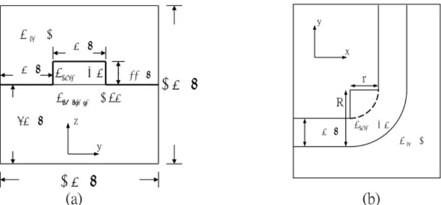
The strong light confinement in high refractive-index contrast structures allows the design of waveg-uide components that can perform complex wavegwaveg-uide interconnections within a small area. In recent progress, these so-called photonic wires [1], which are conventional optical waveguides with sub-micron dimensions and a high refractive-index contrast between the guiding core and surrounding cladding, suffer low bending losses. Manolatous et al [2] have proposed and studied numerous sharp-bend devices modified by adding a resonant structure at the corner. These structures are viewed as two-port resonant system connected to waveguides. Their behavior can be understood using coupling of modes in time and verified by the two-dimensional (2-D) Finite-Difference Time-Domain (FDTD) method. In this work, we examine 90◦-bend photonic wires with a quarter-ring/disk at the corner by utilizing the 3-D FDTD
method. The wire structure we simulate is a silicon guiding layer with rectangular shape of width 500 nm and height 220 nm sitting on a buffer layer of silicon dioxide of thickness 750 nm as illustrated in Figure 1. 0.75 0.75mmmm 0 . 1 = air n 45 . 1 = substrate n 5 . 3 = core n 1.5 1.5mmmm 0.5 0.5mmmm 0.22 0.22mmmm 0.5 0.5mmmm 1.5 1.5mmmm 0.5 0.5mmmm ncore=3.5 0 . 1 = air n
Figure 1. (a) Cross-sectional view and (b) top view of a right-angle bend based on the photonic wire.
MODELING OF PHOTONIC WIRE STRUCTURES
The 3-D FDTD modeling of a photonic wire structure is quite computing resources demanding. It is almost impossible to run 3-D simulations on a single personal computer (PC). In recent years, the conceptual High Performance Computing (HPC) has been realized by parallel computing performed on a computer cluster which is based on the connection of a set of computing nodes. The idea of parallel computing is to divide the whole task into several pieces of sub-tasks and assign those sub-tasks to individual computing nodes. In the implementation of such an approach, the Message Passing Interface (MPI) library [3] has been used to communicate between different nodes and the source program needs
to be parallelized. We have successfully developed 3-D FDTD codes which are able to perform parallel computing.
Since great difference might exist between the real structure and the stucture assumed in the compu-tational domain due to the cubic lattice in the Yee scheme, the Index Average (IA) scheme is adopted to reduce such difference in the dielectric interface. The IA shceme takes the concept of effective dielectric constant corresponding to a weighted area average of the dielectric constant in a cubic cell.
The source excitation is characterized by the calculated mode pattern using the Finite-Difference Frequency-Domain (FDFD) mode solver [4], which is based on the Yee mesh, with an effective index of 2.358 at 1.55-µm carrier wavelength in vacuum. The source in the FDTD computation was a 20-fs wide Gausian pulse modulating the carrier. The grid size is chosen to be 10 nm, which is around one-sixtieth of the guided wavelength, and the time step size is 0.0167 fs. The computational region is 3.5 µm × 5.0 µm × 1.5 µm terminated with 0.05-µm-thick uniaxial perfectly matched layer (UPML) boundaries [5], resulting in totally 4.36-GB RAM consumption.
In order to obtain the transmission, the discrete Fourier transform (DFT) of the electromagnetic (EM) fields along the time history is calculated. Then we use the orthogonality property of waveg-uide modes to calculate the transmittance. The electric field ~E can be written as the superposition of waveguide modes
~ E=X
ν
aνexp(−jβνz) ~eν (1)
where ν is the mode index and βν, and ~eνare the propagation constant and the electric mode field of the
νth mode, respectively. The coefficient of the fundamental mode a1 can be calculated by the integration
over the waveguide cross-section as Z ~ E× ~h1· d~s = Z X ν aνexp(−jβνz) ~eν× ~h1· d~s (2) = a1exp(−jβ1z) Z ~e1× ~h1· d~s (3)
whereR~e1×~h1· d~s with ~h1being the magnetic mode field is known. The integral in (3) is named as the
mode overlap integral. The calculated |a1|2corresponds to the transmittance.
NUMERICAL RESULTS
We perform the simulation on an in-house computer cluster, which contains four computing nodes, each of them is a 3.4-GHz Pentium PC with 1.75-GB RAM. The total 50,000 time-step iterations result in 26 hours of computational time.
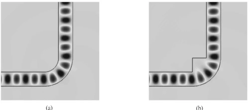
We have tested several radii of the quarter-ring/disk and measured the transmittance for a range of frequencies between 180 THz and 210 THz. Fig. 2 plots the transmittance of the quarter-ring/disk structure with outer radius of 0.6-, 0.8-, 1.0-, and 1.2-µm, respectly. The solid lines and the dash lines show the transmittance calculated with and without the mode overlap integral, respectly. The propagating mode considered is the fundamental TE-like mode. Fig. 3 illustrates the Hzfield distribution
for the quarter-ring/disk structure. The numerical results show that the performance of transmittance depends to a great extent on the radius of the quarter-ring. The larger the radius, the greater the transmittance. Given an outer quarter-ring radius of 1.2 µm, the transmittance exceeds 90 percent. One can see that the dash line is always above the solid line. This is because the mode overlap integral gets rid of the power of radiation modes and only keeps them of the fundamental mode. Similar results are shown in Fig. 2(b) for quarter-disk structures. According to Manolatous et al [2], the quarter-disk plays the role of a “rasonater”. We find that it does not. We may say the EM fields “rasonate” if they reflect forward and backward continuously in a cavity and match the phase condition at the boundary, such as in the Fabry-Perot cavity. In this case, the EM fields pass by along the rim of the disk as one can see in Fig. 3(b), and do not reveal the resonating behavior at the quarter-disk. Another evidence is provided by the transmittance spectrum. If the EM fields resonate, some resonance peaks should exist in the spectrum at resonance frequencies. However, the spectrum is smooth as shown in Fig. 2(b). We thus conclude that the quarter-disk cavity does not behave a resonator in the bending structure and acts much as the quarter-ring does.
Figure 2. The transmittance spectrum of the photonic wire bending with (a) quarter-ring and (b) quarter-disk at the corner.
Figure 3. The snapshot of the Hz field of the photonic wire bending with (a) quarter-ring and (b)
quarter-disk at the corner.
CONCLUSION
The 3-D FDTD method incorporating the IA scheme has been adopted to analyze the photonic wire bends. High performance computing is achieved by parallelizing the 3-D FDTD method. The FDFD mode solver is successfully used as the source excitation in the FDTD computation. The transmitted power is over 90 percent if 1.2-µm-radius quarter-ring is added at the corner. The quarter-disk cavity is found to be not a resonator in the bending structure and behaves much as the quarter-ring does.
REFERENCES
[1] Dumon, P., W. Bogaerts, V. Wiaux, and J. Wouters, “Low-Loss SOI Photonic Wires and Ring Resonators Fabricated With Deep UV Lithography,” IEEE Photonic Technol. Lett. 16, pp. 1328– 1330 (2004)
[2] Manolatou, C., S. G. Johnson, S. Fan, P. R. VIlleneuve, H. A. Haus, and J. D. Joannopoulos, “High-density Integrated Optics,” J. Lightwave Technol. 17, pp. 1682–1692 (1999).
[3] Gropp, W., E. Lusk, and A. Skjellum, Using MPI: Portable Parallel Programming with the Message-Passing Interface, second edition. MIT Press, 1999.
[4] Yu, C. P., and H. C. Chang, “Compact Finite-Difference Frequency-Domain Method for the Analysis of Two-Dimensional Photonic Crystals,” Optics Express. 12, pp. 1397–1408 (2004).
[5] Taflove, A., and S. C. Haness, Computational Electrodynamics: The Finite-Difference Time-Domain Method, second edition.Boston, MA: Artech House, 2000.
FULL-VECTORIAL OPTICAL WAVEGUIDE EIGENMODE SOLVERS BASED ON MULTIDOMAIN PSEUDOSPECTRAL METHODS
Hung-chun Chang*, Po-Jui Chiang, Chu-Sheng Yang, Chin-Lung Wu, and Chun-Hao Teng†
Department of Electrical Engineering, Graduate Institute of Electro-Optical Engineering, and Graduate Institute of Communication Engineering, National Taiwan University
Taipei, Taiwan 106-17, R.O.C.
†now with Department of Mathematics, National Cheng Kung University, Tainan, Taiwan
E-mail: hcchang@cc.ee.ntu.edu.tw
Abstract: A new full-vectorial pseudospectral mode solver based on multidomain pseudospectral methods for
optical waveguides with arbitrary step-index profile is presented. Both Legendre and Chebyshev collocation methods are employed. The multidomain advantage helps in proper fulfillment of dielectric interface conditions, which is essential in achieving high numerical accuracy. The solver is applied to the calculation of guided modes on optical fiber, D-shaped fiber, and rib waveguide, and comparison with analytical results or reported ones based on other methods is made. It is demonstrated that numerical accuracy in the effective index up to the remarkable 10–8 order can be easily achieved.
1. INTRODUCTION
High-accuracy calculation of full-vectorial modes on optical waveguides are important in the design of some waveguide structures and related waveguide devices, and such calculation has been achieved by different numerical methods, e.g., the finite difference method [1]–[3] and the finite element method [4]. In this paper, we present a novel method with remarkably high accuracy, the pseudospectral mode solver (PSMS) which is based on multidomain pseudospectral methods. The multidomain advantage also helps in proper fulfillment of dielectric interface conditions, which is essential in achieving high numerical accuracy. The pseudospectral method has long been applied to fluid dynamics problems [5] and has recently attracted more attention as an alternative technique for computational electromagnetics due to its high-order accuracy and fast convergence behavior over traditional methods while keeping formulation simplicity. Applications to the analysis of electromagnetics in time domain [6] and in frequency domain [7] have both been reported. However, while the theory of pseudospectral method has been well elaborated, the application to frequency-domain problems has not received much focus compared with that to time-domain ones in electromagnetics community. We propose waveguide mode solving schemes utilizing the multidomain Legendre or Chebyshev collocation method together with the curvilinear mapping technique to facilitate and ameliorate the analysis. The Chebyshev and Legendre polynomials are appropriate for different circumstances depending on whether integral or derivative formula will be used. The formulation is derived in the form of an eigenvalue problem so that the modes can be readily obtained by available mathematical tools. As numerical examples, we will consider the optical fiber, the D-shaped fiber, and the
rib waveguide to demonstrate the remarkable performance of the proposed scheme.
2. THE PSMS FORMULATION
We consider an isotropic and homogeneous optical waveguide of arbitrary shape with piecewise uniform refractive index n. By applying the Legendre or Chebyshev collocation method, the governing Helmholtz equation (∇2+ k
02n2)H = β2H
K K
under the
H-formulation can be converted into a matrix eigenvalue problem in the form H = β2H
A , where A denotes the operator matrix, H =[HxT, HyT]T with
T denoting matrix transpose and Hx and Hy being
column vectors, and β is the modal propagation constant. The major step in the conversion into the matrix equation makes use of the fact that the spatial derivatives of a function at a collocation point can be determined by a matrix operation on the values of the function at all the collocation points. The Chebyshev and Legendre polynomials will be appropriate for different circumstances depending on whether one is working on integral or derivative formula.
We discuss and compare the Legendre and Chebyshev collocation methods. The Legendre polynomial PN(x) of order N is defined as (1/2N
N!)(dN/dxN)(x2 – 1)N, where |x| ≤ 1, and the collocation
points are the Legendre-Gauss-Lobatto points defined as the roots of the polynomial (1 – x2 )P′
N (x). The
Chebyshev polynomial TN (x) of order N is defined as
TN (x) = cos (N cos– 1x), where, again, |x| ≤ 1, and the
collocation points are the Chebyshev-Gauss-Lobatto points which are defined as the roots of the polynomial (1 – x2)T'
N. The Legendre approach has
the disadvantage that there exists no analytical formula for these roots which can only be obtained numerically. However, we can benefit from the utilization of the Gauss-Lobatto quadrature formula to significantly simplify the integration of
electromagnetic fields, e.g., when the power flow over surface needs to be determined. In the contrary, although there exists analytical formula for collocation points in the Chebyshev approach, given by xi = – cos (iπ/N), i = 0, 1, 2, …, N, there is no
convenient way to integrate electromagnetic fields as the Legendre approach does. The main advantage of the PSMS lies in that Legendre and Chebyshev collocation methods can provide us with an exceptionally accurate means to calculating the function f(x) and its derivative by the construction of global Legendre-Lagrange and Chebyshev-Lagrange interpolating polynomials LN of order N as (LN f)(x) =
Σi = 0 ~ N f(xi) gi (x). The interpolating
Legendre-Lagrange polynomials are given by gi (x) = – [(1 –
x2 )P′
N (x)] / [N(N + 1)(x – xi) PN(xi)] and the
interpolating Chebyshev-Lagrange polynomials are given by gi (x) = – [(1 – x2 )T ′N (x)( – 1)i + 1] / [ciN2(x –
xi)], where c0 = cN, and ci = 1 for 1 ≤ i ≤ N – 1. Note
that by (LN f)(xi) = f(xi), the spatial derivatives of f(x)
at a collocation point xi can be obtained by a matrix
operation, with the matrix entries Dij = g′j (xi) and d
f(xi)/dx = ΣNj = 0 g′j (xi)f(xj) = Σ Nj = 0 Dij f(xj). For the
Chebyshev approach, the explicit expressions for Dij
as given in [5] are (ci /cj)[(– 1)i + j/(xi – xj)] for i ≠ j, – xi
/[2(1 – xi2)] for 1 ≤ i = j ≤ N – 1, – (2N2 + 1) /6 for i = j
= 0, and (2N2 + 1) /6 for i = j = N.
With the chosen interpolation polynomial, we can finally convert the differentiation operator in the Helmholtz equation into the operator matrix A for
the eigenvalue problem and then treat the required boundary conditions.
3. TREATMENT OF INTERFACE CONDITIONS
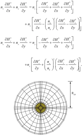
To obtain high-accuracy full-vectorial modal solutions for optical waveguides, proper fulfillment of dielectric interface conditions is essential, whether it is based on the finite difference method [2], [3], the finite element method [4], or others. In the pseudospectral method formulation, one feasible boundary setting is to apply the popularly employed Dirichlet and Neumann type boundary conditions. In electromagnetics, they simply correspond to continuity of electrical and magnetic fields, which, for the H-formulation, could be easily derived from Maxwell's equations as n Hˆ× Ga = n Hˆ× Gb and
ˆ a =
n H⋅ G n Hˆ⋅ Gb, with nˆ =n
xˆx + nyˆybeing the unit
vector normal to the interface and the superscripts a and b denoting adjacent regions (domains). In our numerical scheme, we combine the adjacent regions (domains) by deliberately imposing both types of boundary conditions on the two sides of the interface to guarantee numerical stability. The general form of the Dirichlet type boundary condition appears as Hxa =
Hxb and Hya = Hyb, and that of the Neumann type
boundary condition can be derived as
Fig. 1 Mesh and domain division profile for the step-index optical fiber.
4. NUMERICAL EXAMPLES 4.1 Optical Fiber
We first apply the new SPMS to analyze a step-index optical fiber with core radius a = 2 µm, core-index n1 = 1.46, and cladding index n2 = 1.456,
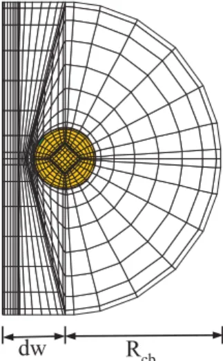
operating at the wavelength λ = 0.6328 µm. for which there exists analytical solution for comparison. Figure 1 shows the typical domain and mesh division profile for the Legendre method where nine sub-domains are adopted. The mesh division profile for the Chebyshev method would be slightly different. Since the dielectric interfaces are made falling on the borders of sub-domains, not all sub-domains are of rectangular shape and proper curvilinear mapping technique has been utilized for transformation between the rectangular coordinate and the curved one of a general sub-domain [8]. The radius of the computational-domain boundary is taken to be Rcb =
11 µm. Figure 2 shows the relative error in effective index (i.e., β divided by the free-space wavenumber) of the fundamental HE11 mode with respect to the
number of unknowns for both the Chebyshev and Legendre spectral methods. It can be seen that both of them yield high-order accuracy and fast convergence
= a b a a b y y x x x x x x H H H H H n n n x y y x y ∂ ∂ ∂ ∂ ∂ + − + + ∂ ∂ ∂ ∂ ∂
2 a b b y a y x y b H n H H n x n x y ∂ ∂ ∂ + − − ∂ ∂ ∂
= a a a b b y y x x y x x y H H H H H n n n x y y x y ∂ ∂ ∂ ∂ ∂ + − + + ∂ ∂ ∂ ∂ ∂
2.
b a b y x a x x b H H n H n y n x y ∂ ∂ ∂ + + − ∂ ∂ ∂
Rcbbehavior over traditional techniques. The exact analytical value of the effective index up to the 10–8
order is 1.45784234. With the Legendre method and the number of unknowns being 6498, we obtain the same effective index value. For strongly-guiding fibers, e.g., with core-index 1.515, and cladding index 1.0, we have also achieved the same 10–8 order
accuracy. The accuracy in fact can be further improved by using finer discretization grids.
Fig. 2 Relative errors in the effective index for the fundamental mode in a step-index optical fiber with the Legendre's and Chebyshev's spectral methods, respectively.
Fig. 3 Cross-section of a D-shaped fiber.
Fig. 4 Mesh and domain division profile for the D-shaped fiber of Fig. 3.
4.2 D-Shaped Fiber
We also consider the D-shaped fiber structure, a fiber with one side polished to produce the D-shaped cladding. As shown in Fig. 3, the refractive indices of the core, the cladding, and the air region are taken as
n1 = 1.46, n2 = 1.456, and n3 = 1, respectively. As in
the first example, the radius of the core is 2 µm, Rcb =
10 µm, and λ = 0.6328 µm. The distance between the core and the polished interface is a variable denoted as d. As shown in Fig. 4, the computational window is divided into 13 sub-domains and the distance between the core and the left side of the computational window is dw = 4 µm. We analyze the structures with d = 0.5 µm and d = 1 µm and consider both the x-polarized and y-polarized fundamental modes. The calculated effective indices using 9386 unknowns are shown in Table 1, with the corresponding results using the improved full-vectorial finite difference method [3] also listed. It is seen that the two methods agree with each other in effective index accuracy up to the 10–7 order, and
both are better than the finite difference analysis without using the improved scheme for treating the dielectric interfaces [9] for which the accuracy is found to be only up to the 10–5 order.
Table 1. Effective indices of the Hx
11 and Hy11
modes for the D-shaped fiber of Fig. 3 with different d’s from [3] and the present PSMS
d (µm) n [3] n [PSMS] 0.5 (Hy) 1.4576733 1.45767329 0.5 (Hx) 1.4576863 1.45768633 1.0 (Hy) 1.4577666 1.45776657 1.0 (Hx) 1.4577725 1.45777254 4.3 Rib Waveguide
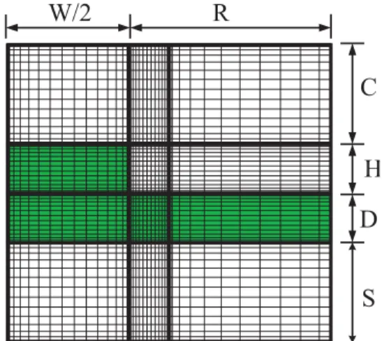
Since the result based on the Chebyshev spectral method has better accuracy and faster convergence than that based on the Legendre method as shown in Subsection 4.1, we will adopt the Chebyshev method in the analysis of the rib waveguide shown in Fig. 5. Due to the symmetry of the mode field, we only need to calculate half of the whole region and one domain and mesh division profile employing 12 sub-domains is shown in Fig. 6. We assume the same parameters as in [2]: the operating wavelength λ = 1.15 µm, rib width W = 3.0 µm, H + D = 1.0 µm with D varying from 0.1 to 0.5 µm, and the refractive indices of the cover nc, the guiding layer ng, and the substrate ns
being 1.0, 3.44, and 3.4, respectively. The parameters for the computational window are R = 3.0 µm, C = 1.0 µm, and S = 5.0 µm. Table 2 shows the effective indices of the fundamental Hy
11mode for different
values of D obtained by Hadley [2] and by the present PSMS with 7680 total unknowns. It is seen that in this multi-corner case, the PSMS confirms the 10–6 Rcb dw 1000 1500 2000 2500 3000 3500 4000 4500 5000 10−9 10−8 10−7 10−6 10−5 Legendre Chebyshev
Relative error in effective index
accuracy in the effective index of [2]. It should be noted that the PSMS uses much easier boundary setting compared to the more sophisticated dielectric corner treatment in the finite difference method of [2].
Fig. 5 Cross-section of a rib waveguide.
Fig. 6 Mesh and domain division profile for the rib waveguide of Fig. 5.
Table 2. Effective indices of the Hy
11 mode for
the rib waveguide of Fig. 5 with different Ds from [2] and the present PSMS
D (µm) n[2] n[PSMS] 0.1 3.412126 3.4121263876 0.2 3.412279 3.4122792728 0.3 3.412492 3.4124926601 0.5 3.413132 3.4131332450 5. CONCLUSION
We have presented a new pseudospectral mode solver (PSMS) for solving Helmholtz equation for optical waveguide modes. The solver is based on the multidomain pseudospectral method with Lengendre or Chebyshev polynomials which are employed to expand spatial derivatives of field functions at collocation points such that Helmholtz equation leads to a numerically solvable eigenvalue problem. The numerical stability and accuracy have been
guaranteed by imposing alternative Dirichlet and Neumann types of boundary conditions between adjacent sub-domains. We have shown that the PSMS promises expeditious convergence speed and superior accuracy over traditional mode solvers for waveguides of arbitrary step-index profile. In the numerical examples of optical fiber and D-shaped fiber, it is demonstrated that numerical accuracy in the effective index up to the 10–8 order is easily
achieved. In the analysis of the multi-corner rib waveguide, the PSMS confirms the 10–6 accuracy in
the effective index reported in [2]. However, the PSMS uses much easier boundary setting compared to the more sophisticated dielectric corner treatment in the finite difference method of [2]. The PSMS is thus a very powerful and flexible technique for analyzing diverse optical waveguides.
ACKNOWLEDGEMENT
This work was supported in part by the National Science Council of the Republic of China under grant NSC93-2215-E-002-036 and in part by the Ministry of Economic Affairs of the Republic of China under grant 91-EC-17-B-08-S1-0015.
REFERENCES
[1] G. R. Hadley, “High-accuracy finite-difference equations for dielectric waveguide analysis I: Uniform regions and dielectric interfaces,” J.
Lightwave Technol., vol. 20, pp. 1210–1218,
2002.
[2] G. R. Hadley, “High-accuracy finite-difference equations for dielectric waveguide analysis II: Dielectric corners,” J. Lightwave Technol., vol. 20, pp. 1219–1232, 2002.
[3] Y. C. Chiang, Y. P. Chiou, and H. C. Chang, “Improved full-vectorial finite-difference mode solver for optical waveguides with step-index profiles,” J. Lightwave Technol., vol. 20, pp. 1609–1618, 2002.
[4] M. Koshiba and Y. Tsuji, “Curvilinear hybrid edge/nodal elements with triangular shape for guided-wave problems,” J. Lightwave Technol., vol. 18, pp. 737–743, 2000.
[5] C. Canuto, M. Y. Hussani, A. Quartweoni, and T. Zang, Spectral Methods in Fluid Dynamics. New York: Springer-Verlag, 1987.
[6] J. S. Hesthaven, P. G. Dinesen, and J. P. Lynov, “Spectral collocation time-domain modeling of diffractive optical elements,” J. Comput. Phys., vol. 155, pp. 287–306, 1999.
[7] Q. L. Liu, “A spectral frequency-domain (PSFD) method for computational electromagnetics,”
IEEE Trans. Antennas Propagat., vol. 50, pp.
131–134, 2002.
[8] W. J. Gordon and C. A. Hall, “Transfinite element methods: Blending-function interpolation over arbitrary curved element domains,” Numer. Math., vol. 21, pp. 109–129, 1973.
[9] Y. L. Hsueh, M. C. Yang, and H. C. Chang, “Three-dimensional noniterative full-vectorial beam propagation method based on the alternating direction implicit method,” J.
Lightwave Technol., vol. 17, pp. 2389–2397,