國
立 交 通 大 學
電機學院微電子奈米科技產業研發
碩士班
碩
士 論 文
氟鈍化效應在高介電常數複晶矽層間介電
層特性及可靠度研究
Characteristics and Reliabilities Research of Fluorine
Passivation Effect on Inter-Poly High-k Dielectrics
研
究 生:陸冠文 Kuan-Wen
Lu
指導教授:羅正忠
博士 Dr.
Jen-Chung
Lou
氟鈍化效應在高介電常數複晶矽層間介電
層特性及可靠度研究
Characteristics and Reliabilities Research of Fluorine
Passivation Effect on Inter-Poly High-k Dielectrics
研
究 生:陸冠文 Kuan-Wen
Lu
指導教授:羅正忠
博士 Dr.
Jen-Chung
Lou
國 立 交 通 大 學
電機學院微電子奈米科技產業研發碩士班
碩 士 論 文
A ThesisSubmitted to College of Electrical and Computer Engineering National Chiao Tung University
In partial Fulfillment of the Requirements For the Degree of
氟鈍化效應在高介電常數複晶矽層間介電層
特性及可靠度研究
研究生 : 陸冠文 指導教授 : 羅正忠 博士 國立交通大學電機學院產業研發碩士班 摘要根據半導體的微縮定律,隨著系統晶片(System on Chip, SOC)的半導體製
造逐漸的微小化,持續降低 CMOS 元件中的閘極介電層及非揮發性記憶體
(non-volatile memories)中的複晶矽層間介電層(inter-poly dielectric)厚度,以達 到高元件密度及低操作電壓的趨勢。傳統的極薄二氧化矽介電層因量子穿遂效應 而導致極大的直接穿遂漏電流,對整個元件產生了可靠度的問題。為了解決這嚴 重的直接穿遂漏電流現象,本篇論文利用高介電常數材料(high-κ)來替換傳統 的二氧化矽。因為高介電常數材料在相同的等效二氧化矽厚度之下,有較大的實 際物理厚度可以抵擋因量子的穿遂效應而產生的直接穿遂漏電流。 但使用高介電常數材料仍有遭遇其它的缺點。例如:在相同的二氣化矽電 壓下,高介電常數材料有較高的界面狀態產生及較多的電荷補捉,這對於元 件操做時臨限電壓的漂移有嚴重的影響。本篇論文利用高介電常數材料做為
介電層,並用氟摻雜的鈍化處理來討論對複晶矽層間電容的影響。在複晶矽 層成長後以離子佈值的方式來植入氟摻雜,使氟原子在後續的高溫摻雜的活 化過程中,使其擴散至複晶矽和複晶矽層間的高介電常數材料(high-κ)介電 層。利用氟的摻入探討有機金屬化學氣相沉積(metal organic chemical vapor deposition)所成長的三氧化二鋁(Al2O3)和二氧化鉿(HfO2) 來改進其可靠度和 元件特性。
我們提出了以矽表面氟離子值入法(silicom surface fluorine implantation),將 氟離子導入複晶矽和複晶矽層間的高介電常數材料(high-κ)介面處。從實驗結 果可充份證明,含氟摻雜的元件有較低的界面狀態產生,和較少的電荷補抓,對 三氧化二鋁和二氧化鉿複晶矽層間電容,不論是漏電流、電子補捉率、崩潰電場 和崩潰電荷,及熱穩定度,複晶矽層間電容的特性都有顯著的提昇。本篇論文中, 非揮發堆疊記憶體的懸浮閘(Floating Gate,FG) 和控制閘(Control Gate,CG) 最好 的氟劑量條件分別為5e13 cm-2 和5e15 cm-2。對於元件的可靠度和穩定性有明顯
的改善。因此,等效氧化層厚度為5 奈米及 3 奈米的三氧化二鋁和二氧化鉿將是
Characteristics and Reliabilities Research of Fluorine
Passivation Effect on Inter-Poly High-k Dielectrics
Student : Kuan-Wen Lu Advisors : Dr. Jen-Chung Lou
Industrial Technology R & D Master Program of Electrical and Computer Engineering College
National Chiao Tung University
Abstract
According to the semiconductor scaling rule, for the semiconductor made of system on a chip (SOC) has become very little gradually, a continuously scaling of the gate dielectrics for complementary metal oxide semiconductor (CMOS) and inter-poly dielectrics (IPD) for electrically-erasable programmable read only memory (EEPROM) and stacked –gate flash memory is needed to achieve high density and low operation voltage trend. In tradition, the ultra-thin silicon dioxide (SiO2) which the quantum effect and then cause more directly tunneling current, which is the issue of the reliability in all devices. In order to solve seriously directly tunneling current, this dissertation is to apply the high dielectric constant materials to replace SiO2. Because high dielectric constant materials compare with SiO2 at the same equivalent oxide thickness (EOT), have thicker physical thickness which can resist directly
But using the high dielectric constant materials still has experienced other problems. For example , high dielectric constant materials have higher interfacial states and charge traps, these will cause more serious threshold voltage shift when working device as the same voltage compare with SiO2.In this thesis, we used high-k materials serving as the IPDs and tunnel dielectrics (TDs) on the stacked-gate flash memories. The influence of fluorine passivation effects on IPD capacitance was investigated. At post-IPD deposition, we incorporate fluorine with fluorine implantation method which was subsequently diffused into the IPD and high-k materials of tunnel dielectrics. The objective of this dissertation was to apply the fluorine incorporation to discuss deposition aluminum oxide (Al2O3) and hafnium oxide (HfO2) with metal organic chemical vapor deposition (MOCVD) for improving reliability and device characteristics.
We describe the characteristics of silicon surface fluorine implantation (SSFI) for IPD and high-k materials interface with incorporation of fluorine. By experimenting, we found that lower generation rate of interface states and lower charge trapping rate are observed for device with fluorine incorporated. For Al2O3 and HfO2 inter-poly capacitors, the sample exhibits optimal quality in terms of leakage current, electron trapping rate, effective breakdown field and charge-to-breakdown (QBD) and the thermal stability of high temperature, the IPDs characteristics result of improving effect significantly. In this thesis, we investigated the most effective fluorine dosage condition respectively is 5e13cm-2 and 5e15cm-2 on floating gate, (FG) and control
誌 謝
從小到大,一路的求學生涯中的學歷,最後要在交通大學碩士班劃上句 點。回顧這十多年來的學生生涯中,我最要感謝我的爸爸和親人所給我的鼓勵和 無後顧之憂的支持。使我能不操心生活的經濟問題,專心求學。在我的碩士班生 涯中,首先要感謝我的指導教授羅正忠博士。謝謝教授肯收我為學生成為實驗室 的成員。和由於有老師在專業課程上指導和研究領域上的協助,讓我養成應有的 研究態度和正確的研究方法。並讓我受益良多更加成長。在這邊,我要向老師至 呈上最衷心的感謝。另外,我要感謝帶我的實驗室陳永裕學長,我接實驗室國科 會計劃,沒有陳永裕學長在我實驗遇到困難和人生低潮時的幫忙和鼓勵,讓我才 能順利的完成研究。也感謝國家奈米實驗室提供製程機台和裡面勞苦功高的工程 帥。 另外要特別感謝交大其它實驗室的學長和同學,鄧志剛、鄭淳護、張明峰、 黃菘宏、李振銘、吳淑華及曾幫助過我的同學等。若沒有和妳們討論研究和你們 的幫忙,我的實驗不會進展的那麼順利,謝謝你們。同時也要感謝在實驗室同屆 中曾一起打拼、互相扶持的同學信富、佳華、元凱、國洲、承修、岳展、嘉宏, 讓我在碩士班留下許多回億。尤其是,信富、佳華,同屆中幫助我很多,真是非 常感激你們。 最後,要對我的父母、家人說聲謝謝,這麼多年來,你們總是默默的為 家裡付出,讓我沒後顧之憂地完成我的學業。在此向所有幫助過我的人致上最深 的敬意,祝福大家都身體健康、平安、快樂。Contents
Abstract (in Chinese) ... I Abstract (in English) ... III Acknowledgements ... V Contents ... VI Table Captions ... VIII Figure Captions ... IX
Chapter 1 Introduction ...1
1.1 Background ...1
1.2 Motivation ...6
1.3 Organization of the Thesis ...10
Chapter 2 Characteristics of Al2O3 Inter-Poly Dielectrics with Fluorine Passivation ………... 17
2.1 Introduction ... 17
2.2 Experimental Details ... 19
2.3 Results and Discussions ... 20
2.3.1 The Basic Electrical Properties on the MOCVD Al2O3 IPD... 20
2.4 Summary ... 28
Chapter 3 Characteristics of HfO2 Inter-Poly Dielectrics with Fluorine Passivation……….... 49
3.1 Introduction ... 49
3.2 Experimental Details ... 52
3.3 Results and comparison between Al2O3 andHfO2……….. 53
3.3.1 Basic Electrical Properties ...53
3.3.2 Electric Field and Leakage Current Density Characteristics ... 54
3.3.3 Relation of Trapping Density and Defect... 55
3.3.4 Reliability Characteristics...56
3.3.5 Temperature Characteristics of the fluorine passivation...57
3.4 Summary ... 58
Chapter 4 Conclusions and Recommendations for Future Works …………... 79
4.1 Conclusions ... 79
4.2 Recommendations for Future Works ... 80
References ... 81
Table Captions
Chapter 1
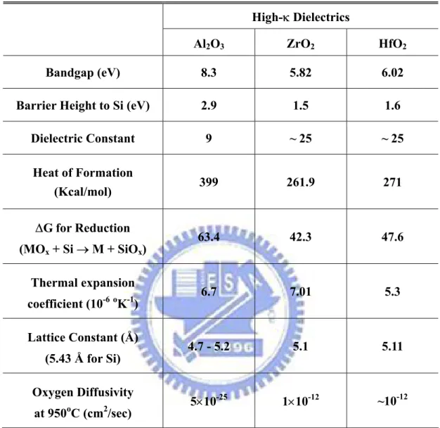
Table 1.1 Materials properties of high-κ dielectrics, Al2O3, ZrO2 and HfO2
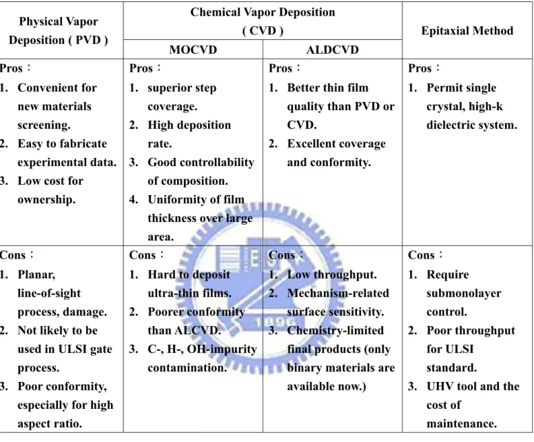
Table 1.2 Comparisons of deposition technique: sputtering, ALD, MOCVD and MBE
Chapter 2
Table 2.1 EOT, κ-value, interfacial layer thickness, effective breakdown field and 63%-failure QBD values of the Al2O3 capacitors with surface fluorine passivation under positive and negative CVS at various fluorine dosage effects.
Chapter 3
Table 3.1 EOT, κ-value, effective breakdown field and 63%-failure QBD values of the HfO2 capacitors with surface fluorine passivation under positive and negative CVS at various fluorine dosage effects.
Figure Captions
Chapter 1
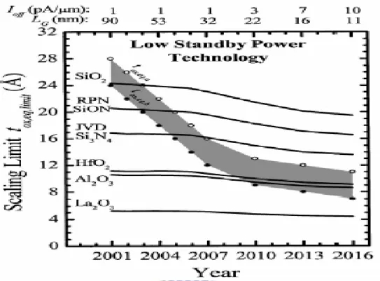
Fig. 1.1 Scaling limits of various gate dielectrics as a function of the technology specifications for low stand-by power technologies.
Fig. 1.2 Leakage current density and EOT projection of nitrided oxides from ITRS roadmap 2004 update.
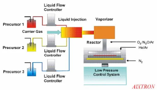
Fig. 1.3 A schematic diagram of typical MOCVD system structure. Fig. 1.4 Band alignment of topical high-k dielectrics.
Chapter 2
Fig. 2.1 Cross-sectional view of Al2O3 inter-poly capacitors with surface fluorine passivation . The fluorine was implanted on Poly-I (Floating Gate) and Poly-II (Control Gate).
Fig. 2.2 Key process steps of Al2O3 inter-poly capacitors with surface fluorine passivation.
Fig. 2.3 (a) Floating Gate C-V curves. C-V characteristics of Al2O3 floating gate inter-poly capacitors with surface fluorine passivation effect is beneficial in scaling EOT that fluorine dosage ranging from 1e12cm-2 to 1e14cm-2 at 10keV. Fig. 2.3 (b) Control Gate C-V curves . C-V characteristics of Al2O3 floating gate inter-poly capacitors with surface fluorine passivation effect is beneficial in scaling EOT that fluorine dosage ranging from 5e13cm-2 to 5e15cm-2 at 20keV.
Fig. 2.4 (a) J-V characteristics of Al2O3 floating gate inter-poly capacitors with surface fluorine passivation effect is beneficial in suppressing low-field leakage current density that fluorine dosage ranging from 1e12cm-2 to 1e14cm-2 at 10keV. Fig. 2.4 (b) J-V characteristics of Al2O3 control gate inter-poly capacitors with surface fluorine passivation effect is beneficial in suppressing low-field leakage current density that fluorine dosage ranging from 5e13cm-2 to 5e15cm-2 at 20keV.
Fig. 2.5 As-fabrication trap densities evaluation at 2 V constant voltage stress (CVS) of Al2O3 floating gate inter-poly capacitors with surface fluorine passivation effect that fluorine dosage ranging from 1e12cm-2 to 1e14cm-2 at 10keV under (a) positive 2V (b) negative 2V trap densities.
Because of the process was outdiffusion by rapid thermal annealing (RTA) three time in Floating Gate.
Fig. 2.5 As-fabrication trap densities evaluation at 2 V constant voltage stress (CVS) of Al2O3 control gate inter-poly capacitors with surface fluorine passivation effect that fluorine dosage ranging from 5e13cm-2 to 5e15cm-2 at 20keV under (c) positive 2V (d) negative 2V trap densities. Al2O3 inter-poly capacitors with fluorine passivation can reduce As-fabrication trap densities.
Fig. 2.6 QBD Weibull plots of Al2O3 inter-poly dielectric with surface fluorine passivation effect under (a) positive CVS and (b) negative CVS that fluorine dosage ranging from 1e12cm-2 to 1e14cm-2 at 10keV . Al2O3 inter-poly capacitors with surface fluorine passivation effect can lightly increase QBD in floating gate.
Fig. 2.6 QBD Weibull plots of Al2O3 inter-poly capacitors with surface fluorine passivation effect under (c) positive CVS and (d) negative CVS that fluorine dosage ranging from 5e13cm-2 to 5e15cm-2 at 20keV. Al2O3 inter-poly dielectric with surface fluorine passivation effect can significantly increase QBD in Control Gate.
Fig. 2.7 Temperature dependence of gate current density at 3 MV/cm of Al2O3 inter-poly capacitors with surface fluorine passivation that fluorine dosage ranging from 1e12cm-2 to 1e14cm-2 at 10keV in floating gate under (a) positive and (b) negative polarities.
Fig. 2.7 Temperature dependence of gate current density at 3 MV/cm of Al2O3 inter-poly capacitors with surface fluorine passivation that fluorine dosage ranging from 5e13cm-2 to 5e15cm-2 at 20keV in control gate under (c) positive and (d) negative polarities.
Fig. 2.8 Band diagrams of Al2O3 inter-poly capacitors with surface fluorine passivation under (a) positive and (b) negative gate voltage biased to the Poly-II.
Fig. 2.9 The average EOT of Al2O3 IPD capacitors with surface fluorine passivation under(a) floating gate (b) control gate (c) floating gate and control gate compared.
Fig. 2.12 The dosage-average breakdown voltage images of Al2O3 capacitors with surface fluorine passivation under (a) Positive VG floating gate and control gate compare (b) Negative VG floating gate and control gate compare.
Fig. 2.13 The effect breakdown field of Al2O3 capacitors with surface fluorine passivation under floating gate and control gate compared.
Fig. 2.14 The charge to breakdown (QBD) images of Al2O3 capacitors with surface fluorine passivation under (a) Positive VG (b) Negative VG floating gate and control gate compare.
Fig. 2.15 The temp images of Al2O3 capacitors with surface fluorine passivation under (a) Positive VG (b) Negative VG floating gate and control gate compare.
Fig. 2.16 The FIB cross-sectional images of Al2O3 inter-poly capacitors.
Fig. 2.17 The FIB top images of Al2O3 inter-poly capacitors thickness must be smaller than 500Å to do HRTEM.
Fig. 2.18 The TEM all cross-sectional images of Al2O3 inter-poly capacitors.
Fig. 2.19 The TEM cross-sectional images of Al2O3 inter-poly capacitors about 100Å ~120Å. (a) without fluorine. (b) FG with 5E13 cm-2 (c) CG with 5E15 cm-2.
Chapter 3
Fig. 3.1 Cross-sectional view of HfO2 inter-poly capacitors with surface fluorine passivation. The fluorine was implanted on Poly-I (Floating Gate) and Poly-II (Control Gate).
Fig. 3.2 Key process steps of HfO2 inter-poly capacitors with surface fluorine passivation.
Fig. 3.3 (a)C-V characteristics of HfO2 floating gate inter-poly capacitors with surface fluorine passivation effect is beneficial in scaling EOT that fluorine dosage ranging from 1e12cm-2 to 1e14cm-2 at 10keV. (b) C-V characteristics of HfO2 control gate inter-poly capacitors with surface fluorine passivation effect is beneficial in scaling EOT that fluorine dosage ranging from 5e13cm-2 to 1e15cm-2 at 20keV.
Fig. 3.4 The average EOT of HfO2 IPD capacitors with surface fluorine passivation under(a) floating gate (b) control gate (c) floating gate and control gate compared.
Fig. 3.5 The Capacitance of HfO2 IPD capacitors with surface fluorine passivation under floating gate and control gate compared.
capacitors coupling ratio.
Fig. 3.7 (a) J-V characteristics of HfO2 floating gate inter-poly capacitors with surface fluorine passivation effect is beneficial in suppressing low-field leakage current density that fluorine dosage ranging from 1e12cm-2 to 1e14cm-2 at 10keV. Fig. 3.4 (b) J-V characteristics of HfO2 control gate inter-poly capacitors with surface fluorine passivation effect is beneficial in suppressing low-field leakage current density that fluorine dosage ranging from 5e13cm-2 to 1e15cm-2 at 20keV.
Fig. 3.8 The dosage-average breakdown voltage images of HfO2 capacitors with surface fluorine passivation under (a) Positive VG floating gate (b) Negative VG floating gate (c) Positive VG control gate (d) Negative VG control gate.
Fig. 3.9 The dosage-average breakdown voltage images of HfO2 capacitors with surface fluorine passivation under (a) Positive VG (b) Negative VG floating gate and control gate comparison.
Fig. 3.10 The effective breakdown field of HfO2 capacitors with surface fluorine passivation under floating gate and control gate comparison.
Fig. 3.11 (a) The fluorine concentration and depth profiles for the three individual implants, and their sum for 1% fluorine in 1500 SiO2 film [94]. (b) SIMS depth profile of 19 F- in the local F sample before and after FGA (4oo℃, 30 min). F tends to segregate at HfO2/ SiO2 interface after FGA. F diffuses toward HfO2/ SiO2 interface [95].
Fig. 3.12 As-fabrication trap densities evaluation at 2 V constant voltage stress (CVS) of HfO2 Floating Gate inter-poly capacitors with surface fluorine passivation effect that fluorine dosage ranging from 1e12cm-2 to 1e14cm-2 at 10keV under (a) positive 2V (b) negative 2V trap densities. The effect of fluorine passivation is bad than without fluorine passivation. Because of the process was outdiffusion by rapid thermal annealing (RTA) three time in Floating Gate.
Fig. 3.12 As-fabrication Positive trap densities evaluation at 2 V constant voltage stress (CVS) of HfO2 Control Gate inter-poly capacitors with surface fluorine passivation effect that fluorine dosage ranging from 5e13cm-2 to
inter-poly capacitors with surface fluorine passivation effect can lightly increase QBD in Floating Gate .
Fig. 3.13 QBD Weibull plots of HfO2 inter-poly capacitors with surface fluorine passivation effect under (c) positive CVS and (d) negative CVS that fluorine dosage ranging from 5e13cm-2 to 1e15cm-2 at 20keV. HfO2 inter-poly dielectric with surface fluorine passivation effect can significantly increase QBD in Control gate .
Fig. 3.14 The charge to breakdown (QBD) images of HfO2 capacitors with surface fluorine passivation under (a) Positive VG (b) Negative VG floating gate and control gate compare.
Fig. 3.15 Temperature dependence of gate current density at 1.73 MV/cm of HfO2 inter-poly capacitors with surface fluorine passivation that fluorine dosage ranging from 1e12cm-2 to 1e14cm-2 at 10keV in Floating Gate under (a) positive and (b) negative polarities.
Fig. 3.15 Temperature dependence of gate current density at 1.73 MV/cm of HfO2 inter-poly capacitors with surface fluorine passivation that fluorine dosage ranging from 5e13cm-2 to 1e15cm-2 at 20keV in Control Gate under (c) positive and (d) negative polarities.
Fig. 3.16 The Temperature images of HfO2 capacitors with surface fluorine passivation under (a) Positive VG (b) Negative VG floating gate and control gate compare.
Fig. 3.17 The FIB cross-sectional images of HfO2 inter-poly capacitors. Fig. 3.18 The TEM all cross-sectional images of HfO2 inter-poly capacitors.
Fig. 3.19 The TEM cross-sectional images of HfO2 inter-poly capacitors about 150Å with FG 5E13 cm-2 sample.
CHAPTER 1
Introduction
1.1 Background
As the scaling rule keeps going, the dimension of gate oxide for complementary metal oxide semiconductor (CMOS) has decreased dramatically for the past decade. The integrated circuit technology nowadays makes devices with high density and low operation voltage for the system-on-chip (SOC) application. We want such requirements like high performance (speed), low static (off-state) power and a wide range of power supply and output voltages [1], The density of devices on silicon chip has been following the “Moore’s law”. It meant that doubling the circuit density about every two or three years since 1980 [2]-[4]. The density improvement combines ont only the progress in lithography but also the innovation in device fabrication technology. Form this trend results in a dramatic expansion in technology and communication markets including the market associated with high-performance microprocessor and low static-power applications, such as wireless systems. Because
thermodynamically and electrically stable high-quality Si-SiO2 interface as well as superior electrical isolation properties by using thermally grown amorphous SiO2 as the gate dielectric. ~1010 cm-2 defect charge density, ~1010 cm-2eV-1 midgap interface state density and 15 MV/cm hard breakdown field are routinely obtained and therefore expected in spite of dimensions. These outstanding electrical properties clearly present a significant challenge for any other alternative gate dielectric candidates [5], [6].
Over the years, the industry, demand for greater integrated circuit functionality and performance for lower cost and increased circuit density, this has translated into a higher density of transistors on a wafer. So, there have been several major evolutions in silicon digital logic technology. The MOS technology, expecially CMOS technology became the most important digital logic technology for all IC industry, and silicon is the main semiconductor material[7].The scaling of oxide thickness has long been recognized as one of determinant factor for devices scaling. High driving current and thereby improved performance can be achieved by reducing the oxide thickness. At the current rate of progressing, Figure 1.1 show the scaling limits of various gate dielectrics trends from the published 2003-ITRS roadmap (International Technology Roadmap for Semiconductor). The imperative need for a nitrided oxide (SiOxNy) and high dielectric constant (κ) gate dielectrics for low standby power application after the year 2002 and 2006, respectively [8]. However, the direct tunneling current increases exponentially by about one order of magnitude for every 0.2nm ~ 0.3nm reduction in oxide thickness. This additional leakage current not only causes increased power dissipation but also affect the circuit functionality due to the decreased operation margins.
For this reason, several alternative materials for silicon dioxide are currently being investigated. Ultrathin nitrided oxides are, at this moment, the best choices to replace pure SiO2 [9]-[15]. Figure 1.2 shows the expected equivalent oxide thickness (EOT) trends from the published 2004-ITRS roadmap. It indicated that nitrided oxides can extend SiO2 limitation to 2006 without massive change in production technologies. Nitrided oxides have several properties superior to those of conventional thermal SiO2, and it deserves to mention the suppression of boron penetration from the poly-Si gate and enhanced reliability. Nitrogen also reduces hot-electron-induced degradation [16]. The dielectric constant of the oxynitride increases linearly with the percentage of nitrogen from κ (SiO2) = 3.9 to κ (Si3N4) = 7.8 [17], though one should note that most SiOxNy films grown currently by thermal methods are lightly doped with N (< 10 at.%) and therefore have a dielectric constant only slightly higher than that of pure SiO2. The other potential candidates to replace silicon dioxide are high-κ materials, including aluminum oxide (Al2O3), hafnium oxide (HfO2) and zirconium oxide (ZrO2) etc [18]-[21]. The most important advantage of high-κ dielectric is the several orders reduction of magnitude of leakage current compared to SiO2 at the same EOT. However, in device performance point of view, a suitable gate dielectric candidate should also meet the other requirements, including high thermal stability, high carrier mobility, small oxide charges, good stress immunity and CMOS compatible.
[30]-[33]. By increasing the floating gate coupling ratio, high-κ IPD can lead to a high electric field across tunnel oxide (TOX) even at very low control gate voltage. For the tunnel dielectric engineering of stacked-gate flash memories, the issue is closely related to dielectric material selection itself. Flash tunnel dielectric has two roles. One is a barrier to suppress charge leakage under read and retention. Second role is a charge transfer path. In order to avoid trap-assisted tunneling via one trap site, the minimum TOX thickness of conventional FG structure will be limit to 8 nm. This limits the tunnel SiO2 scaling and program/erase voltage reduction. Nitrided oxides have been intensively studied, but so far only 5 to 10 times improvement for low field leakage is achieved [34]. This is not enough, because it only achieves 1 nm reduction even with suit fluorine dosage.
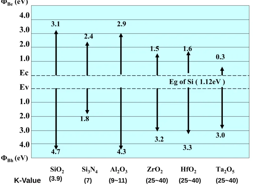
Figure 1.4 shows the calculated band offsets for most high-k dielectrics. To successfully employ the high-κ IPD and TD into flash memory, one must take charge retention issues into consideration and make sure that the barrier height (ϕB) between Si and the new adopted high-κ dielectrics should be larger than 1.5eV for effectively suppressing the loss of floating gate charges through electron thermal emission [34]. Usually, dielectrics with higher κ inherently have lower ϕB. Therefore a trade-off between dielectric constant and barrier height is inevitably required in trying to implement the high-κ dielectrics in flash memories.
As the scaling of flash memories devices have developed, high-k dielectrics instead of conventional silicon dioxide or oxy-nitrides. Because high-k materials can maintain the same EOT in thicker physical thickness, therefore they can resist effectively for the direct-tunneling current to across the insulator and reduces the amount of off-state leakage current density [35].
The relationship between dielectrics constant and thickness is followed:
3.9×ε
o
×Α
C
m [eq-1]
EOT =
K
ox
× t
high-k
[eq-2]
K
high-k
=
EOT
The continuing miniaturization of stacked-gate flash memory devices requires inter-poly dielectrics (IPD), the dielectrics constants (k) of which are larger than the conventional used silicon dioxide. Example of such high-k materials are aluminum oxide (Al2O3) [18], hafnium oxide (HfO2) [36][37], zirconium oxide (ZrO2) [38] [39], Table 1-1 summarizes the properties of potential high-k candidates.
Among high-k materials, HfO2 and Al2O3 are the most promising candidates due to high k (HfO2~25) and large band gap (Al2O3~6.02eV) respectively. They are suitable to be integrated into DRAM process. Because they are researched in this
1.2 Motivation
In the early age of DRAM development, two dimensional cell structure was widely applied on the DRAM cell. Memory cell capacitance plays a important role, which can determine the data retention time, store charge, writer and erase speed. In the design bit generation, the minimum cell capacitance should be 25fF/cell. The measure of capacitance capacity can be described as the following equation:
C =
ε
0ε
rA/d
Where
C:
the dielectric capacitanceε
0:
the vacuum permittivityε
r:
the relative dielectric constant of dielectric materialA:
the surface area of capacitord:
the dielectric thicknessIn order to get high memory density and high capacitance in the DRAM chip,increasing the surface area of capacitor and the relative dielectric constant of dielectric material can be used to increase capacitance. Three-dimensional cell structure was introduced to 4MB-above generation, trench capacitor cell and stacked capacitor cell (STC). Both of the trench and the stacked cell techniques are still used in commercial DRAM products now. Three-dimension cell structure of DRAM increases the surface area of capacitor to get high capacitance; nevertheless, it is not
dimension shrinking with high-k materials.
As memory trend develop in future. The low-power nonvolatile memories control are important trend in communication products. In the recent flash memory technologies, short program/erase times and operating voltage reductions are the most important issues to realize high speed/low power operation [29], [40]-[42]. For EEPROM and flash memory devices, the IPD requires a high charge-to-breakdown (QBD), high breakdown field and low leakage current to obtain good data retention characteristics [43]-[45]. It is not sufficient to meet the stringent data retention requirement of IPD while applying fluorine passivated silicon surface technologies due to the unavoidable leakage current [46]. In order to accomplish this without a trade-off between low power and high speed operations, high coupling ratio should be achieved by increasing the floating gate capacitance [47]-[54].
There are three different approaches can be used to increase coupling ratio. First, decrease the IPD thickness. Oxide/nitride/oxide (ONO) multi-layered films had been extensively investigated and frequently used as the dielectric layer in the flash memory devices and other applications [55]-[57]. However, decreasing the thickness of the IPD to increase the coupling ratio may cause serious leakage and reliability problems which are fatal in the retention time of flash memories. Secondly, increase the area of the IPD capacitor. High capacitive-coupling ratio cell [47]-[49], 3-dimension inter-poly dielectric [51], and hemisphere grain [52], [53] had been proposed to effectively increase the capacitance area and lower the control gate bias.
Therefore, it is straightforward and effective to incorporate alternative high dielectric constant (high-κ) materials on nonvolatile memories to replace oxide/nitride/oxide IPD for increasing floating gate capacitance without increasing cell area and complexity of fabrication while suppressing charge loss. By increasing the floating gate coupling ratio, high-κ IPDs can lead to a high electric field across tunnel oxide even at very low control gate voltage.
Recently, aluminum oxide (Al2O3) [18], [66]-[68] and hafnium oxide (HfO2) [21], [69]-[72] had been proved as promising candidates for the gate dielectrics of sub-0.1 µm device due to their higher κ, relatively high ϕB and superior thermal stability, shown in Table 1.1. Thanks to the high dielectric constant and high thermal stability, Al2O3 and HfO2 are suitable to be integrated into stacked-gate flash memories. Nonetheless, the effects of these kinds of high-κ dielectrics on flash memories are seldom investigated. To further realize the dielectric properties of these high-κ dielectrics, some reliability issues such as breakdown field, charge trapping and temperature-dependence behaviors are extensively studied for both gate dielectric and flash memories applications.
Many deposition methods such as physical vapor deposition (PVD), metal-organic chemical vapor deposition (MOCVD), atomic layer chemical vapor deposition (ALCVD) [73], [74], and molecular beam epitaxial method (MBE), etc. have been employed to prepare high-κ IPDs. The pros and cons of each deposition techniques are demonstrated in Table 1.2. For industrial application, PVD and MBE are not appropriate tools for high-κ film deposition. Since MOCVD has the advantage of superior step coverage, high deposition rate, good controllability of composition, excellent uniformity of film thickness over large area, we, therefore, choose the
structure is shown in Fig. 1.3. The MOCVD chamber is equipped with a turbomolecular pump and a liquid injection system, which has four independent-controlled injectors. The latter is consisted of a liquid pump to pump the precursors through a hot nickel frit with a proper rate because the pump is unreliable at low pump rates. The vapors are carried with a 200sccm flow of Ar to a gas distribution ring which is located at a proper distance from the substrate. In contrast to the conventional bubble system, the liquid injection is with sufficient temperature window to alleviate the thermal aging of the precursor. This is because the precursor remains in liquid state at room temperature until it is pumped into the vaporizer and injected into the deposition chamber. However, the precursor should be kept at long-term chemical stability in solvent and non-reactive with other precursors solvent [75], [76]. The components of the vaporizer, the gas ring and the connecting tube are maintained at a temperature of 190ºC with heating tapes and blankets, while the substrate temperature is controlled at 500ºC with quartz-halogen lamps and a thermocouple. A rotating suspensor is used for uniform heating during processing. A flow of 100sccm N2 is maintained throughout the deposition cycle. The base pressure of the MOCVD chamber is ~10-8Torr. The deposition pressure of the deposition is at the 5mTorr where the gas-phase collisions are scarce.
As many reports indicated, the direct contact of high-κ materials and Si-substrate will be imperfect and debatable. The dominance of the Si MOSFETs over competing technologies has largely been attributed to the high quality of thermally grown SiO2
interface due to the strong vertical electric field present in the channel. For maintaining the excellent transport properties at the Si interface, a possible method to suppress the interfacial layer thickness is to passivate the Si surface before the high-κ IPD deposition. One of the methods is to passivate the Si surface with fluorine implant surface, then nitrogen-contained ambient activation. Passivation of the Si surface using fluorine treatment after the deposition of polysilicon has been shown to be effective in achieving the low EOT and preventing the boron penetration [78], [79]. However, this technique results in higher interface charges which leads to higher hysteresis and reduced channel mobility [80]. The Si-F is a superior barrier for H2O and oxygen, and it can suppress oxygen to diffuse into Si substrate [78]. After the fluorine passivation treatment, a thin interlayer layer ( ﹤20 Å ) was deposited and measured by optical measurement system ( Ellipsometer ). As reports, passivation of the Si surface is prior to the deposition of high-κ gate dielectrics and it shows the result to achieve the low EOT and increase reliability by making the interface smoother [81].
1.3 Organization of This Thesis
There are five chapters in this thesis. In chapter 1, we present a conceptive introduction to describe the background of the semiconductor technology and discuss the possible issues that we may meet during the dimension scaling down. In addition, we would concern about the hopeful solutions to overcome the physical limits in the ITRS, discuss and explain the reasons for high-κ IPD application in the nonvolatile
In chapter 2, the effects of fluorine passivation on inter-poly characteristics of MOCVD Al2O3 dielectrics are examined. The basic electrical properties, electric field, leakage current, and reliability characteristics are presented and discussed.
In chapter 3, the effects of fluorine passivation on inter-poly characteristics of MOCVD HFO2 dielectrics are examined. The basic electrical properties, electric field, leakage current, and reliability characteristics are presented and discussed.
Finally, in chapter 4, the conclusions are made and the recommendations describe the topics which can be further researched .
Table 1.1 Materials properties of high-κ dielectrics, Al2O3, ZrO2 and HfO2.
High-κ Dielectrics
Al2O3 ZrO2 HfO2
Bandgap (eV) 8.3 5.82 6.02
Barrier Height to Si (eV) 2.9 1.5 1.6
Dielectric Constant 9 ~ 25 ~ 25 Heat of Formation (Kcal/mol) 399 261.9 271 ∆G for Reduction (MOx + Si → M + SiOx) 63.4 42.3 47.6 Thermal expansion coefficient (10-6oK-1) 6.7 7.01 5.3 Lattice Constant (Å) (5.43 Å for Si) 4.7 - 5.2 5.1 5.11 Oxygen Diffusivity at 950oC (cm2/sec) 5×10 -25 1×10-12 ~10-12
Table 1.2 Comparisons of deposition techniques: sputtering, ALD, MOCVD and MBE.
Chemical Vapor Deposition ( CVD ) Physical Vapor Deposition ( PVD ) MOCVD ALDCVD Epitaxial Method Pros: 1. Convenient for new materials screening. 2. Easy to fabricate experimental data. 3. Low cost for
ownership. Pros: 1. superior step coverage. 2. High deposition rate. 3. Good controllability of composition. 4. Uniformity of film
thickness over large area.
Pros:
1. Better thin film quality than PVD or CVD. 2. Excellent coverage and conformity. Pros: 1. Permit single crystal, high-k dielectric system. Cons: 1. Planar, line-of-sight process, damage. 2. Not likely to be
used in ULSI gate process.
3. Poor conformity, especially for high aspect ratio. Cons: 1. Hard to deposit ultra-thin films. 2. Poorer conformity than ALCVD. 3. C-, H-, OH-impurity contamination. Cons: 1. Low throughput. 2. Mechanism-related surface sensitivity. 3. Chemistry-limited final products (only binary materials are available now.) Cons: 1. Require submonolayer control. 2. Poor throughput for ULSI standard.
3. UHV tool and the cost of
Fig. 1.1 Scaling limits of various gate dielectrics as a function of the technology specifications for low stand-by power technologies [Ref. 7].
Fig. 1.2 Leakage current density and EOT projection of nitrided oxides from ITRS roadmap 2004 update.
Fig. 1.4 Band alignment of topical high-k dielectrics.
Barrier Height to Si
Eg of Si ( 1.12eV )
Ф
Be(eV)
4.0
3.0
2.0
1.0
Ec
Ev
1.0
2.0
3.0
4.0
Ф
Bh(eV)
SiO
2Si
3N
4Al
2O
3ZrO
2HfO
2Ta
2O
5(3.9)
3.0
0.3
2.9
4.3
1.5
3.2
3.3
1.6
1.8
2.4
3.1
4.7
K-Value
(7)
(9~11)
(25~40)
(25~40)
(25~40)
CHAPTER 2
Characteristics of Al
2O
3Inter-Poly Dielectrics
With Fluorine Passivation
2.1 Introduction
Recently, Devices with high dielectric constant materials (high-k dielectrics materials) such as aluminum oxide (Al2O3)have been studied intensively. However, investigation of the materials shows that fluorine dopant penetration through dielectrics is a significant problem due to the improved characteristics and reliability.
In tradition, ultra-thin oxide will undergo tunneling effect and then cause gate leakage current, which cause reliability probes. High dielectric constant materials, Al2O3 are used to replace SiO2 has widely studied. Compare with SiO2 at the same equivalent oxide thickness (EOT), high dielectric constant materials have thicker physical thickness which can stop from tunneling effect, and avoid more leakage current. Using the high dielectric constant materials is expected to have reduced leakage current and increase breakdown field and the charge-to-breakdown (QBD) as
in the Al2O3 inter-poly dielectrics (IPD) film with the poly surface fluorine implantation (PSFI) method. The incorporation of fluorine atoms into the Al2O3 inter-poly dielectrics (IPD) film reduces not only interface dangling bonds but also bulk traps, which is responsible for the improvements in electrical properties. Among these materials, Al2O3 inter-poly dielectric is a promising candidate because of its compatibility with Fluorine implantation.
With the scaling down of thickness of the inter-poly dielectrics (IPD), the quality of dielectric becomes very critical for the application of the EEPROM and flash nonvolatile memories. Lower leakage of the dielectric means longer data retention time. As many reports indicated that high dielectric constant materials with fluorine implantation has been shown improved electrical properties [82]-[84]. It is found that the incorporation of fluorine on the bottom poly-Si surface can not only reduce leakage current by one order of magnitude, but also enhance the breakdown field and the charge-to-breakdown (QBD) as well. This is ascribed to the resultant smoother interface between the dielectric and the floating gate by surface fluorine passivation and less electron charge traps in the bulk. However, the QBD is better than other only sputter and NH3 nitridation method. Moreover, the effect of fluorine dosage on the electrical properties and reliability characteristics of Metal Organic Chemical Vapor Deposition (MOCVD) Al2O3 inter-poly capacitors with surface fluorine passivation are studied in this chapter. The electrical properties of the Al2O3 IPD are strongly influenced by the fluorine passivation. The optimum floating gate is 5e13cm-2 and control gate is 5e15cm-2 in terms of leakage current, electron trapping rate and QBD.
2.2 Experimental Details
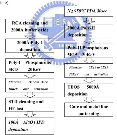
The n+-polysilicon/Al2O3 IPD/n+-polysilicon capacitors were fabricated on 6-inch p-type (100)-oriented silicon wafers. Silicon wafer was thermally oxidized at 980oC to grow a 2000Å buffer oxide. 2000Å bottom polysilicon film (Poly-I) was deposited on the buffer oxide by low pressure chemical vapor deposition (LPCVD) system using SiH4 gas at 620oC and subsequently implanted with phosphorous at 5e15cm-2, 20keV and implanted with fluorine dosage ranging from 1e12cm-2 to 1e14cm-2 at 10keV. Then activated with N2 RTA at 950°C for 30s. Prior to the growth of Al2O3 IPDs, the native oxide covered Poly-I was cleaned by the conventional RCA cleaning and diluted HF etching in sequence for the removal of particles and native oxides. The surface of Poly-I prepared in this matter was known to be contamination free and terminated with atomic hydrogen. After being wet cleaned and dipped in HF solution, and 10nm Al2O3 IPD was deposited by Metal-Organic Chemical Vapor Deposition (MOCVD) system at 500°C with Ar/O2 ambient. Annealing of aluminum oxide (Al2O3) IPDs was carried out by rapid thermal annealing (RTA) at 950oC temperatures ranging in an N2 atmosphere for 30s. Subsequently, a 2000Å top polysilicon layer (Poly-II) was deposited by LPCVD and implanted with phosphorous at 5e15cm-2, 20keV. Then, implanted with fluorine dosage ranging from 5e13cm-2 to 5e15cm-2 at 20keV. Dopants were then activated with N2 RTA at 950°C for 30s.
LCR meter. Moreover, the physical thickness was estimated by high resolution transmission electron microscopy (HRTEM). The electrical properties and reliability characteristics of the inter-poly capacitors were measured using a HP4156C semiconductor parameter analyzer.
2.3 Results and Discussions
In this chapter, the Characteristics and Reliabilities of Fluorine Passivation Effect on the MOCVD Al2O3 capacitors with various Fluorine Dosage show to investigated in terms of store of capacitance, leakage current and dielectric reliabilities.
2.3.1 The Basic Electrical Properties on the MOCVD Al2O3 IPD
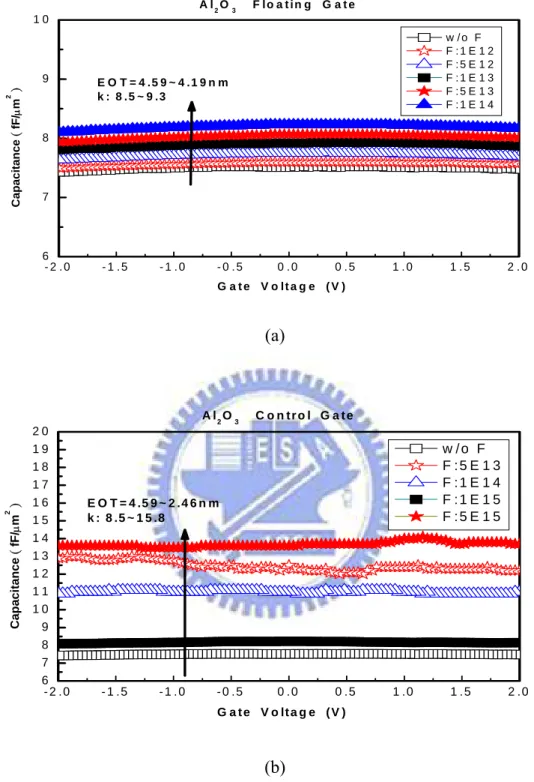
Figure 2.3(a) shows the high frequency C-V curves (1MHz) of the floating Gate (FG) corresponding EOT of Al2O3 inter-poly capacitors with surface Fluorine Passivation Effect that fluorine dosage ranging from 1e12cm-2 to 1e14cm-2 at 10keV. Figure 2.3(b) shows the high frequency C-V curves (1MHz) of the control Gate (CG) corresponding EOT of Al2O3 inter-poly capacitors with surface fluorine passivation Effect that fluorine dosage ranging from 5e13cm-2 to 5e15cm-2 at 20keV. The EOT is decreased as raising Fluorine passivation effect, which can be ascribed to the fluorine itself physical factors. Because of fluorine atoms inter wafer lattices and to fill vacancy and cause AlF3 formation, therefore are able to increased capacitance. As the fluorine dosage of floating gate continually increases to 1e14cm-2 and the fluorine
defects and slightly increase permittivity, smaller EOT value is therefore obtained as compared effectively with 1e14cm-2 and 5e15cm-2 samples.
2.3.2 Electric Field and Leakage Current Density Characteristics
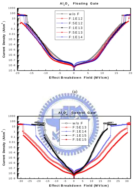
Figure 2.4(a) and Figure 2.4(b) that compares the J-E characteristics of the Al2O3 inter-poly capacitors with fluorine Passivation at various fluorine dosage. It is found that the sample with floating gate fluorine 5e13cm-2 and control gate 5e15cm-2 can effectively reduce the low-field leakage current about one to two orders of magnitude than other samples, which is helpful to increase effective breakdown field from the floating gate and control gate sample. The leakage current in negative polarity is smaller than that in positive polarity due to asymmetric band diagram. It can be explained by the reduced damage generated and assistance in the interface of the inter-poly dielectrics and polysilicon film. Because thermal stress and atoms impact on lattice of crystalcause various crystal defects that like interstitial impurity atoms, edge dislocation, self- interstitial, dislocation loop, vacancy etc. Using fluorine passivation not only can reduce defect but also increase electrical properties.
2.3.3Relation of Trapping Density and Defect
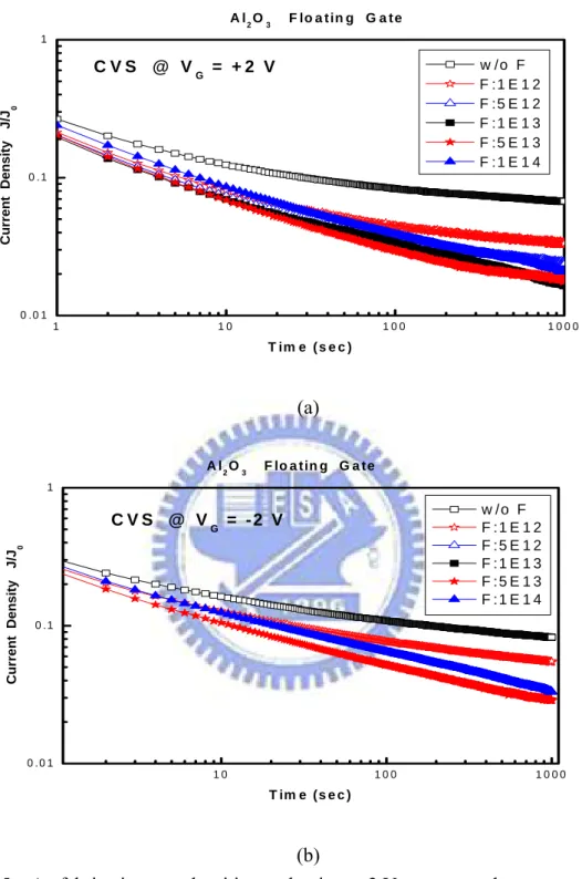
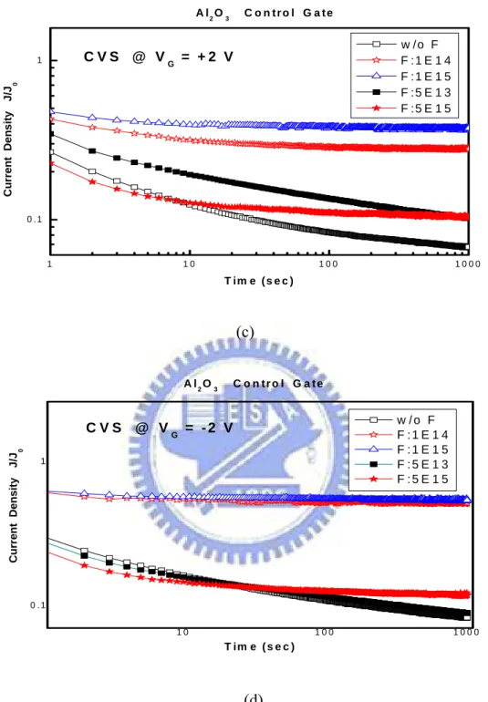
fluorine dosage ranging from 5e13cm-2 to 5e15cm-2 at 20keV. Presents the transient currents for the fluorine passivation effect of Al2O3 IPDs under a low field of 2 MV/cm in order to suppress the creation of stress-induced traps. Filling of the pre-existing electron traps in the high dielectric constant materials leads to the decrease of the current leakage magnitude over time for all samples [85], [86]. Moreover,the rate of leakage current reduction in either polarity is nearly identical, suggesting that the traps are distributed uniformly across the films. Incorporation of Fluorine atoms tends to segregate at Poly and Poly/ HfO2 interfaceafter activation. The N2 950℃ can effectively assist the crystal lattice atoms arranges in order again, and the stress levels on the fluorine implanted case are consistently higher which result from the much stronger Al-F bonds relative to Al-Al, Al-O or even Al-Si bonds. The Al-F bonds strength are 159Kcal/mole whereas the Al-Al bonds strength are only 45 Kcal/mole. This is perhaps manifest best in the relative melting points of AlF3 (1291℃) than Al (660℃) or other bonds samples. Therefore, we believe that the dependence of the IPD characteristic on fluorine passivation effect is closely related to the bulk defects in the high-k dielectric. Figure 2.5(c) , Figure 2.5 (d) show the 100Å Al2O3 gate dielectric under a 2V constant voltage stress (CVS) for 1000 sec, and good reliability evidenced to show fluorine passivation is better than without fluorine passivation from the small current charge and stress-induced leakage current (SILC) respectively. Moreover, Al2O3 inter-poly capacitors fluorine passivation effect exhibits small electron trapping rate than without fluorine passivation effect. But in Figure 2.5(a) , Figure 2.5 (b) the fluorine passivation effect is bad than without fluorine passivation. Because of the process was outdiffusion by rapid thermal annealing (RTA) three time in Floating Gate. The result of the process produced more defect and influenced electrical properties characteristics.
2.3.4 Reliability Characteristics
Figure 2.6(a), Figure 2.6 (b) show QBD Weibull plots of Al2O3 inter-poly capacitors with surface fluorine passivation effect in positive and Negative CVS that fluorine dosage ranging from 1e12cm-2 to 1e14cm-2 at 10keV in floating Gate. The Weibull distributions of the charge-to-breakdown (QBD) field in both polarities as the magnitude of gate bias is 5.7MV/cm. Effective charge to breakdown(QBD) field exhibits nearly independent in various fluorine dosage. Because the process was outdiffusion by rapid thermal annealing (RTA) three time in floating gate, so caused more dangling bond and defects in the crystal. The increase of most fluorine passivation effect was due to the increase of fluorine dosage magnitude in floating gate. But fluorine dosage 1e14cm-2 was too much, and 1e12cm-2 , 5e12cm-2 was not enough to reach to fit the process of floating gate. This was ascribed to the resultant not smooth interface between the high dielectric and the floating Gate polysilicon by more or less fluorine implantation caused stress defect. The fluorine dosage 5e13cm-2 sample had best performance in preventing charge loss from floating Gate. The lesser leakage current means that retaining data time longer and higher charge breakdown field.
Figure 2.6(c), Figure 2.6 (d) show QBD Weibull plots of Al2O3 inter-poly capacitors with surface fluorine passivation effect in positive and negative 5.7MV/cm
bonds. For positive and negative gate bias, capacitors with fluorine surface passivation effect can significantly increase charge-to-breakdown (QBD) characteristics one order compared without fluorine passivation effect at 5e15cm-2 dosage in control gate inter-poly capacitors.
We believe that the dependence of the IPD characteristic on fluorine passivation is closely related to the bulk defects in the high dielectric material. In control gate, fluorine passivation can effectively reduce dislocation, voied, vacancies, interstitial and dangling bond result in the less interface defect density. By the result of QBD can evidence that 5e15cm-2 dosage is the optimized dosage at 20keV in control gate.
2.3.5 Temperature Characteristics of the fluorine passivation Al2O3 IPD
Figure 2.7(a) , Figure 2.7 (b) show illustrates the temperature dependence of gate current density at 3 MV/cm of Al2O3 inter-poly capacitors with surface fluorine passivation that dosage ranging from 1e12cm-2 to 1e14cm-2 at 10keV in floating gate. Figure 2.7(c) , Figure 2.7 (d) show illustrates the temperature dependence of gate current density at 3 MV/cm of Al2O3 inter-poly capacitors with surface fluorine passivation that dosage ranging from 5e13cm-2 to 5e15cm-2 at 20keV in control gate. In general, floating gate and control gate samples reduce about one order leakage current density, exhibited considerably weak measuring temperature dependence on the leakage current density in either polarity. By the Figures implying that the tunneling mechanism for the Al2O3 IPD is Fowler Nordheim-like, rather than Frankel Poole-like. On the other hand, the magnitude of the leakage current was found to be strongly depended on the fluorine passivation temperature. As high temperature, the electron obtained more energy and surpassed the energy barrier of Poly-I to inject into
InPoly-II/high-k dielectric/ Poly-I sandwich structure, the interface between the Poly and thehigh-k dielectric thin films plays significant roles by fluorine passivation in the functional performanceof the thin films. It was found that fluorine passivation can effective to resist leakage current density breakdown and promote the Al2O3 IPD performance, because fluorine passivation can mend damaged lattices.
At the process due to the work function differenceof the Poly electrodes, and the degree of asymmetry increaseswith the increasing work function difference. For the samples withhigh work function Poly as both or at least oneof the electrodes, the passivation switching is much faster. Thecurrent–voltage curves at various fluorine dosages indicated the interface-controlled asymmetric phenomena are mainly determined by the Schottky emission and charge injectionat the Poly/high-k dielectric polymer interface in high temperature. Fig. 2.8 Band diagrams of Al2O3 inter-poly capacitors with surface fluorine passivation under (a) positive and (b) negative gate voltage biased to the Poly-II.
2.3.6 Results and Compare
In this chapter, the effects of fluorine passivation on the MOCVD Al2O3 IPDs are investigated in terms of EOT, κ-value, dosage-EOT, dosage-average breakdown current, effective breakdown field and 63%-failure QBD values and temperature under (a) Positive VG (b) Negative VG Floating Gate and Control Gate
passivation effect rising up to 5e13cm-2 in floating gate. Figure 2.9 (a) show over fluorine dosage 1e14 cm-2 is contrary effect that causes more dangling bond easily in Al2O3/poly interface. But in control gate, the fluorine passivation effect can rise up to 5e15cm-2 . This is ascribed to that only polysilicon can store more capacity of fluorine atoms, as seen in Figure 2.9 (b). Besides, we use 20kev in control gate than 10kev in floating gate causing implanted distance farther. Figure 2.9 (c) and Figure 2.10 illustrates show floating gate and control gate compared. The evidences we know, EOT and κ-value of control gate is more effectively than floating gate from the same dosage condition at 5e13 cm-2 or 1e14 cm-2.
Figure 2.11(a), (b), (c), (d), Al2O3 IPD capacitors with fluorine incorporation could also exhibit better dielectric performance and reliability. Incorporation of fluorine into Al2O3/poly interface has been highly effective in lower leakage current and higher breakdown voltage from floating gate than control gate in the same condition. The evidences show in Figure 2.12(a), (b) and Figure 2.13. The stacked-gate flash memories with Al2O3 by using Fowler-Nordheim(FN) tunneling are helpless in operation voltage reduction. In general, the dielectric constant increased, the bandgap decreased. Because we used fluorine passivation to improve device performance and repair defect. By increasing the floating gate coupling ratio, fluorine passivation Al2O3 IPD capacitors can lead to a high electric field across tunnel oxide (TOX) even at very low control gate voltage.
Figure. 2.14 show the charge to breakdown (QBD) images of Al2O3 IPDs with surface fluorine passivation under (a) Positive VG (b) Negative VG Floating Gate and Control Gate compare. We believe that the dependence of the IPD characteristic with fluorine passivation is closely related to the bulk defect s in the dielectric. By fluorine
of suitable fluorine atoms can repair bulk defect, increase data retention, suppress electron trapping rate and interfacial layer growth.
Figure. 2.15 (a),(b) show the Al2O3 IPD capacitors has better performance at high temp. We describe the characteristics with silicon surface fluorine implantation (SSFI)
for Al2O3 IPD films. The thermal stability of Al2O3 IPD capacitors is much improved
owing to the incorporation of fluorine into Al2O3 thin films. The gate leakage current of the
SSFI Al2O3 films is about one to two orders less than that of samples without any fluorine
implantation. In addition, improvements in stress-induced leakage current (SILC) and charge
trapping characteristics are realized in the Al2O3 films with the SSFI. The incorporation of
fluorine atoms into the Al2O3 films reduces not only interface dangling bonds but also bulk
traps, which is responsible for the improvements in properties. These results clearly
reveal Al2O3 floating gate with fluorine passivation can effectively reduce electron loss as well as obtain better average breakdown voltage, high QBD and resist high-temperature than control gate.
As the Al2O3 IPD capacitors process had completed the work. We used high-resolution transmission electron microscopy (HRTEM) to confirm Al2O3 IPD thickness and interfacial layer thickness. Before HRTEM, We must be cutting and digging a hole with focused ion beam (FIB). Figure.2.16 show the FIB cross-sectional images of Al2O3 IPD capacitors. The FIB top images of Al2O3 inter-poly dielectric device thickness must be smaller than 500Å to do HRTEM, show
layer thickness.
2.4 Summary
The effects of fluorine dosage on the electrical properties and reliability characteristics of the Al2O3 inter-poly capacitors with surface fluorine passivation are evaluated in this chapter. It was found that the electrical properties of Al2O3 IPD capacitors strongly depend upon the fluorine passivation effect. The floating gate with 5e13cm-2 and control gate with 5e15cm-2 are respective the best condition for the Al2O3 IPD capacitors electrical characteristics in terms of leakage current, temperature, QBD and electron trapping rate of control gate. The capacitance as increase as fluorine dosage that the consequences indicate closely related to the fluorine passivation effect and fluorine dosage when changing fluorine dosage concentration. The results apparently demonstrate Al2O3 IPD capacitors with surface fluorine passivation effect can effectively reduce charge transfer between control gate and floating gate, better retention and disturb characteristics are expected by replacing ONO IPD to Al2O3 IPD. The Al2O3 dielectric with surface fluorine passivation thus appears to be very promising for future flash memory devices. Table 2.1 lists several physical and electrical parameters, including EOT, κ-value, interfacial layer thickness, and effective breakdown field and 63%-failure QBD values of the Al2O3 IPD capacitors with surface fluorine passivation under positive and negative CVS at various fluorine dosage effects.
Table 2.1 EOT, κ-value, interfacial layer thickness, effective breakdown field and 63%-failure QBD values of the Al2O3 capacitors with surface fluorine passivation under positive and negative CVS at various fluorine dosage effects.
EBD (MV/cm) Interfacial Layer 63% QBD (C/cm2) F Dosage (cm-2) κ EOT (Å)
positive negative Thickness (Å) positive negative
0 8.5 45.9 16.8 16.3 15 2.05 1.91 FG 5E13 9.1 42.8 19.2 18.9 10.5 2.11 2.16 CG 5E15 15.8 24.6 30.1 28.9 7.9 10.23 4.32
P-type Si Substrate 2000Å Buffer Oxide 2000Å n+Poly-I 2000Å n+Poly-II TEOS 5000Å Al Metal Pad SiNx~10Å 100Å Al2O3
Fig. 2.1 Cross-sectional view of Al2O3 inter-poly capacitors with surface fluorine passivation . The fluorine was implanted on Poly-I (Floating Gate) and Poly-II (Control Gate).
N2 950ºC PDA 30sec RCA cleaning and
2000Å buffer oxide 2000Å Poly-II
deposition 2000Å Poly-I
deposition Poly-II Phosphorous
5E15 20KeV Poly-I Phosphorous
5E15 20KeV Fluorine 5E13 to 5E15
20KeV and activation Fluorine 1E12 to 1E14
10KeV and activation TEOS 5000Å
deposition STD cleaning and
HF-last Gate and metal line
patterning 100Å Al2O3 IPD
deposition
Fig. 2.2 Key process steps of Al2O3 inter-poly capacitors with surface fluorine passivation.
- 2 . 0 - 1 . 5 - 1 . 0 - 0 . 5 0 . 0 0 . 5 1 . 0 1 . 5 2 . 0 6 7 8 9 1 0 E O T = 4 . 5 9 ~ 4 . 1 9 n m k : 8 . 5 ~ 9 . 3 A l2O3 F l o a t i n g G a t e C a pac itance ( fF / µ m 2 ) G a t e V o l t a g e ( V ) w / o F F : 1 E 1 2 F : 5 E 1 2 F : 1 E 1 3 F : 5 E 1 3 F : 1 E 1 4 (a) - 2 . 0 - 1 . 5 - 1 . 0 - 0 . 5 0 . 0 0 . 5 1 . 0 1 . 5 2 . 0 6 7 8 9 1 0 1 1 1 2 1 3 1 4 1 5 1 6 1 7 1 8 1 9 2 0 E O T = 4 .5 9 ~ 2 .4 6 n m k : 8 .5 ~ 1 5 .8 A l2O3 C o n t r o l G a t e Capacitance ( fF/ µ m 2 ) G a t e V o lt a g e ( V ) w / o F F : 5 E 1 3 F : 1 E 1 4 F : 1 E 1 5 F : 5 E 1 5 (b)
- 2 0 - 1 5 - 1 0 - 5 0 5 1 0 1 5 2 0 1 E - 9 1 E - 8 1 E - 7 1 E - 6 1 E - 5 1 E - 4 1 E - 3 0 . 0 1 0 . 1 1 1 0 1 0 0 1 0 0 0 A l 2O3 F lo a t in g G a t e w / o F F :1 E 1 2 F :5 E 1 2 F :1 E 1 3 F :5 E 1 3 F :1 E 1 4 Cur re n t Density ( A/cm 2 ) E f f e c t B r e a k d o w n F ie ld ( M V /c m ) (a) - 3 0 - 2 5 - 2 0 - 1 5 - 1 0 - 5 0 5 1 0 1 5 2 0 2 5 3 0 1 E - 9 1 E - 8 1 E - 7 1 E - 6 1 E - 5 1 E - 4 1 E - 3 0 . 0 1 0 . 1 1 1 0 1 0 0 1 0 0 0 A l2O3 C o n t r o l G a t e w / o F F : 5 E 1 3 F : 1 E 1 4 F : 1 E 1 5 F : 5 E 1 5 Cur re n t Density ( A/ cm 2 ) E f f e c t B r e a k d o w n F ie ld ( M V /c m ) (b)
Fig. 2.4 (a) J-V characteristics of Al2O3 floating gate inter-poly capacitors with surface fluorine passivation effect is beneficial in suppressing low-field leakage current density that fluorine dosage ranging from 1e12cm-2 to 1e14cm-2 at 10keV. Fig. 2.4 (b) J-V characteristics of Al2O3 control gate inter-poly capacitors with surface fluorine passivation effect is beneficial in suppressing low-field leakage current density that fluorine dosage ranging from 5e13cm-2 to 5e15cm-2 at 20keV.
1 1 0 1 0 0 1 0 0 0 0 . 0 1 0 . 1 1 C V S @ V G = + 2 V A l2O3 F lo a t in g G a t e C u rr ent Density J/J 0 w /o F F :1 E 1 2 F :5 E 1 2 F :1 E 1 3 F :5 E 1 3 F :1 E 1 4 T im e ( s e c ) (a) 1 0 1 0 0 1 0 0 0 0 . 0 1 0 .1 1 C V S @ V G = - 2 V Cur re nt D e nsity J/ J 0 A l2O3 F lo a t in g G a te w / o F F : 1 E 1 2 F : 5 E 1 2 F : 1 E 1 3 F : 5 E 1 3 F : 1 E 1 4 T im e (s e c ) (b)
Fig. 2.5 As-fabrication trap densities evaluation at 2 V constant voltage stress (CVS) of Al O floating gate inter-poly capacitors with surface fluorine passivation effect
1 1 0 1 0 0 1 0 0 0 0 . 1 1 C V S @ VG = + 2 V A l2O3 C o n t r o l G a t e C u rr e nt De n s ity J/ J 0 w /o F F :1 E 1 4 F :1 E 1 5 F :5 E 1 3 F :5 E 1 5 T im e ( s e c ) (c) 1 0 1 0 0 1 0 0 0 0 . 1 1 C V S @ VG = - 2 V A l2O3 C o n t r o l G a t e Curr ent Density J/J 0 w / o F F : 1 E 1 4 F : 1 E 1 5 F : 5 E 1 3 F : 5 E 1 5 T im e ( s e c ) (d)
Fig. 2.5 As-fabrication trap densities evaluation at 2 V constant voltage stress (CVS) of Al2O3 control gate inter-poly capacitors with surface fluorine passivation effect that fluorine dosage ranging from 5e13cm-2 to 5e15cm-2 at 20keV under (c) positive 2V (d) negative 2V trap densities. Al2O3 inter-poly capacitors with fluorine passivation can reduce As-fabrication trap densities.
1 E - 5 1 E - 4 1 E - 3 0 . 0 1 0 . 1 1 1 0 1 0 0 - 3 - 2 - 1 0 1 2 3 C V S @ V g = + 5 . 7 M V /c m w / o F F : 1 E 1 2 F : 5 E 1 2 F : 1 E 1 3 F : 5 E 1 3 F : 1 E 1 4 A l2O3 F lo a t in g G a t e ln ( -ln ( 1-F) ) C h a r g e t o B r e a k d o w n ( C /c m2 ) (a) 1 E - 5 1 E - 4 1 E - 3 0 . 0 1 0 . 1 1 1 0 1 0 0 - 3 - 2 - 1 0 1 2 3 C V S @ V g = - 5 . 7 M V / c m A l2O3 F lo a t in g G a t e w / o F F : 1 E 1 2 F : 5 E 1 2 F : 1 E 1 3 F : 5 E 1 3 F : 1 E 1 4 ln ( -ln ( 1-F) ) C h a r g e t o B r e a k d o w n ( C /c m2 ) (b)
1 E - 5 1 E - 4 1 E - 3 0 . 0 1 0 . 1 1 1 0 1 0 0 - 3 - 2 - 1 0 1 2 3 A l2O3 C o n t r o l G a t e C V S @ V g = + 5 .7 M V /c m P o s it iv e C V S w /o F F :5 E 1 3 F :1 E 1 4 F :1 E 1 5 F :5 E 1 5 ln ( -ln ( 1-F) ) C h a r g e t o B r e a k d o w n ( C /c m2 ) (c) 1 E - 5 1 E - 4 1 E - 3 0 . 0 1 0 . 1 1 1 0 1 0 0 - 3 - 2 - 1 0 1 2 3 A l2O3 C o n t r o l G a t e C V S @ V g = - 5 .7 M V / c m w / o F F : 5 E 1 3 F : 1 E 1 4 F : 1 E 1 5 F : 5 E 1 5 ln ( -ln ( 1-F) ) C h a r g e t o B r e a k d o w n ( C /c m2 ) (d)
Fig. 2.6 QBD Weibull plots of Al2O3 inter-poly capacitors with surface fluorine passivation effect under (c) positive CVS and (d) negative CVS that fluorine dosage ranging from 5e13cm-2 to 5e15cm-2 at 20keV. Al2O3 inter-poly dielectric with surface fluorine passivation effect can significantly increase QBD in Control Gate.
40 60 80 100 120 1E -7 1E -6 Al2O3 Floating Gate Temperature Cu rren t Den s it y @ 3 MV/ CM ( A/ cm 2 ) w /o F F:1E 12 F:5E 12 F:1E 13 F:5E 13 F:1E 14 V G = +3V (a) (℃) 4 0 6 0 8 0 1 0 0 1 2 0 1 E - 7 1 E - 6 1 E - 5 1 E - 4 A l2O3 F lo a tin g G a te T e m p e ra tu re Cu rr en t De nsi ty @ 3MV /C M ( A/ cm 2 ) w /o F F :1 E 1 2 F :5 E 1 2 F :1 E 1 3 F :5 E 1 3 F :1 E 1 4 VG = -3 V (℃)
4 0 6 0 8 0 1 0 0 1 2 0 1 E - 7 1 E - 6 1 E - 5 A l2O3 C o n t r o l G a t e T e m p e r a t u r e Cu rren t Den s it y @ 3 M V /C M ( A/cm 2 ) w / o F F : 5 E 1 3 F : 1 E 1 4 F : 1 E 1 5 F : 5 E 1 5 V G = + 3 V (℃) (c) 4 0 6 0 8 0 1 0 0 1 2 0 1 E - 7 1 E - 6 1 E - 5 1 E - 4 T e m p e r a tu r e C u rr e n t Density @ 3MV/CM ( A/cm 2 ) w / o F F :5 E 1 3 F :1 E 1 4 F :1 E 1 5 F :5 E 1 5 VG = -3 V A l 2O3 C o n tr o l G a te (℃) (d)
Fig. 2.7 Temperature dependence of gate current density at 3 MV/cm of Al2O3 inter-poly capacitors with surface fluorine passivation that fluorine dosage ranging from 5e13cm-2 to 5e15cm-2 at 20keV in control gate under (c) positive and (d) negative polarities.
Poly-I Poly-II Al2O3IPD - - - - - - I.L. Positive Vg - - - - - - - - - - - (a) - - - - - - Poly-II Poly-I Al2O3IPD I.L. Negative Vg + + + + + + + + + + + + + - impact ionization + - + +
-- -- --4 .0 4 .2 4 .4 4 .6 D o s ag e ( c m-2) 1 E 1 4 5 E 1 3 1E 13 5 E 1 2 1E 12 W /O F Eq uivalent O x id e T h ickness ( nm ) Al 2O3 F lo a tin g G ate w /o F F :1 E 1 2 F :5 E 1 2 F :1 E 1 3 F :5 E 1 3 F :1 E 1 4 (a) 3 .0 3 .5 4 .0 4 .5 5 .0 5 .5 A l2O3 C o n tro l G a te D o s a g e ( c m-2) 5 E 1 5 1 E 1 5 1 E 1 4 5 E 1 3 W /O F Equ iv a len t Oxide Th ick n es s ( nm ) w /o F F :5 E 1 3 F :1 E 1 4 F :1 E 1 5 F :5 E 1 5 (b)
-- -- --3 .0 3 .2 3 .4 3 .6 3 .8 4 .0 4 .2 4 .4 4 .6 w /o F F G F :5 E 1 3 F G F :1 E 1 4 C G F : 5 E 1 3 C G F :1 E 1 4 C G F :5 E 1 5 A l
2O3 F lo atin g G ate a n d C o n tro l G ate
D o s ag e ( c m-2) 1 E 1 4 5 E 1 3 1E 13 5 E 1 2 1E 12 W /O F Eq uivalent O x id e T h ickness ( nm ) (c)
Fig. 2.9 The average EOT of Al2O3 IPD capacitors with surface fluorine passivation under(a) floating gate (b) control gate (c) floating gate and control gate compared.
6 7 8 9 1 0 1 1 1 2 1 3 1 4 1 5 1 6 1 7 1 8 1 9 2 0 w / o F F G F : 5 E 1 3 F G F : 1 E 1 4 C G F : 5 E 1 3 C G F : 1 E 1 4 E O T = 4 .5 9 ~ 2 .6 6 n m k : 8 .5 ~ 1 4 .6 A l2O3 F lo a t in g G a t e a n d C o n t r o l G a t e Capacitance ( fF/ µ m 2 )