Electron traps in organic light-emitting diodes
Min-Jan Tsai and Hsin-Fei Meng
Citation: Journal of Applied Physics 97, 114502 (2005); doi: 10.1063/1.1913800
View online: http://dx.doi.org/10.1063/1.1913800
View Table of Contents: http://scitation.aip.org/content/aip/journal/jap/97/11?ver=pdfcov
Published by the AIP Publishing
Articles you may be interested in
Effects of interfacial stability between electron transporting layer and cathode on the degradation process of organic light-emitting diodes
Appl. Phys. Lett. 91, 223509 (2007); 10.1063/1.2817939
Injection and transport processes in organic light emitting diodes based on a silole derivative
J. Appl. Phys. 99, 084907 (2006); 10.1063/1.2190714
Modeling the influence of charge traps on single-layer organic light-emitting diode efficiency
J. Appl. Phys. 99, 064509 (2006); 10.1063/1.2186374
Capacitance–voltage characterization of polymer light-emitting diodes
J. Appl. Phys. 97, 054504 (2005); 10.1063/1.1857053
Direct observation of deep electron traps in aged organic light emitting diodes
J. Appl. Phys. 97, 024503 (2005); 10.1063/1.1835567
Electron traps in organic light-emitting diodes
Min-Jan Tsai and Hsin-Fei Menga兲
Institute of Physics, National Chiao Tung University, Hsinchu 300, Taiwan, Republic of China
共Received 21 October 2004; accepted 25 March 2005; published online 24 May 2005兲
This work presents the effects of electron traps in organic light-emitting diodes using a model which includes charge injection, transport, and recombination. For electron-only devices, the electron current is reduced by the traps for several orders of magnitude at fixed voltage, and the traps strongly increase the transient time. For bipolar devices, due to negative trapped charges, traps enhance the hole current and the total current, opposite to the electron-only devices. The traps also make the recombination region close to the cathode. There is a voltage-dependent critical trap density beyond which the quantum efficiency decreases and transient time rises dramatically. The quantum efficiency is doubled if the hole traps are added to balance the electron and hole injections. Finally, the trap effect can be used in a bilayer light-emitting diode to make the emission
color-tunable. © 2005 American Institute of Physics.关DOI: 10.1063/1.1913800兴
I. INTRODUCTION
Conjugated polymer light-emitting diode 共PLED兲 has
been of great research interest since 1990共Ref. 1兲 due to its easy processing and mechanical flexibility. PLED comprises a thin layer or multilayer of intrinsic semiconducting lumi-nescent conjugated polymer sandwiched between two elec-trodes. The band gap of organic semiconductor is large
共⬎2 eV兲, so most charge carriers are due to injection from
the electrodes. Hence, the type of electrode determines whether the device is electron-only or hole-only or bipolar. In bipolar devices carriers can move across the device and recombine to emit light. One of the most unique properties of a conjugated polymer is that the hole mobility is much higher than the electron mobility.2,3In fact, this mobility im-balance is expected to be the main limit for the PLED quan-tum efficiency. Interestingly, the imbalance measured by the time-of-flight experiment in thick devices2is generally much stronger than the imbalance observed by space-charge-limited current in thinner devices.4Because the space-charge density is inversely proportional to the square of the film thickness for fixed voltage, the apparent dependence of the imbalance on the film thickness can be attributed to the de-pendence of the effective electron mobility on the electron density. Such dependence suggests the presence of electron traps, which are more easily filled up in thinner devices. In our view, there are two reasons causing the higher hole mo-bility, both related to the electron traps. The first is that the background p-doping compensates for the hole traps caused by the structural defects; the second is that oxidation contrib-utes to electron traps, but not to hole traps.5 In addition to reducing the electron mobility, the electron traps may confine the electroluminescence共EL兲 near the cathode. Metallic elec-trodes are efficient quenching sites for electroluminescence, so this confinement is expected to strongly reduce the per-formance of the device. The imbalanced carrier mobility manifests not only in the absolute value, but also in its
de-pendence on the electric field.3,4 The field dependence of
electron mobility exceeds that of hole mobility, and we be-lieve that this phenomenon can also be explained by the existence of electron traps. Device models have been pro-posed for PLED in steady state6,7and transient.8,9Traps have
also been included in some simple device model.10,11
How-ever, so far, very little is known for the effect of electron traps on the microscopic properties of PLED.
In this paper we present a comprehensive theoretical in-vestigation on the effects of electron traps in polymer de-vices. The mobilities for free electrons and holes are
as-sumed to be equal.5 We employ a device model which
includes explicitly the traps in the continuity equation and Poisson’s equation. In the electron-only devices, higher elec-tron trap density is shown to cause selec-tronger field dependence of the electron current. The traps are shown not only to affect the electron transport, but also to increase dramatically the transient time required for the device to reach the steady state. For hole-only devices without traps the time scale is
microsecond,8 but in electron-only or bipolar devices the
time scale can be in millisecond. For bipolar devices, the influences of traps on the recombination rate, the device ef-ficiency, and the carrier transport are considered. It is surpris-ing that the traps enhance the hole current due to the accu-mulation of a large amount of the negative space charges inside the device. As the trap density increases beyond a certain limit, the quantum efficiency drops sharply due to carrier imbalance. Interestingly, if the hole traps are added to the model to balance the electron and hole injection, the efficiency is recovered.
This paper is organized as follows: Section II discusses the device model with traps. Results and discussions for electron-only, bipolar, and bilayer devices are presented in Sec. III, and Sec. IV draws the conclusions.
II. DEVICE MODEL WITH TRAPS
In this work we assume the exponential energy distribu-tion of traps.10,12–14The trap density of states has the form
a兲Author to whom correspondence should be addressed; electronic mail: [email protected]
0021-8979/2005/97共11兲/114502/7/$22.50 97, 114502-1 © 2005 American Institute of Physics
nt共,x兲 = Nt共x兲
kTt exp
冉
共 − c兲
kTt
冊
, 共1兲where Nt共x兲 is the trap density in position x, kTtis the char-acteristic energy of traps, which is the depth of traps from the conduction band edgec. The free electrons are assumed to be in thermal equilibrium with trapped electrons.15Using Eq.
共1兲 and approximating the Fermi–Dirac distribution as a step
function,15 a relationship between the trapped 共nt兲 and free 共nf兲 electron density can be obtained, which is
nt= Nt
冉
nf n0冊
T/Tt
, 共2兲
where n0is the effective density of states for free electrons.
Equation共2兲 is used in the continuity equation.
A. Single-layer device
In a single-layer device model, the device comprises of a thin-film layer of organic semiconductor sandwiched be-tween two electrodes. The transport of electrons and holes are described by time-dependent continuity equations with drift-diffusion current, coupled with Poisson’s equation. That is nto t = 1 e
冉
Jn x冊
+ G − R, 共3兲 p t = − 1 e冉
Jp x冊
+ G − R, 共4兲 E x = e共p − nf− nt兲 ⑀ , 共5兲 where nto= nf+ nt, 共6兲 and Jn= e冉
nfE + kT e nf x冊
, 共7兲 Jp= e冉
pE − kT e p x冊
. 共8兲Here, ntois the total electron density, including free共nf兲 and trapped 共nt兲 electrons. p is the hole density, Jn 共Jp兲 is the electron共hole兲 current density, and G and R are the genera-tion and recombinagenera-tion rate, respectively; x is the posigenera-tion normal to the film, and the cathode is at x = 0; t is the time, e is the absolute electron charge, andis the free-carrier mo-bility. Note that is the same for electrons and holes. E is the electric field, k is Boltzmann’s constant, T is the tempera-ture, and⑀=⑀0⑀ris the permittivity of the material. The dif-fusion coefficient is expressed in terms of the carrier mobil-ity using Einstein’s relation. Because of the large band gap of these semiconductors, the generation rate G is too small to produce enough carriers compared with injected carriers.6,7 Therefore, G is neglected in our model. The recombination rate R is bimolecular, which takes the form16,17
R = rnfp, 共9兲
where r is Langevin recombination coefficient given by6,7,10
r =e
⑀ . 共10兲
Substituting Eq.共2兲 into 共3兲
nf t = 1 1 + B
冉
1 e Jn x − rnfp冊
, 共11兲 nt t = 1 1 + B冉
1 e Jn x − rnfp冊
, 共12兲 where B = NtT Tt冉
1 n0冊
T/Tt 1 n1−T/Tf t. 共13兲These equations are integrated together with the equa-tion for the electric field6,7
E共x,t兲 t = − 1 L VL t − 1 ⑀
冋
Jt共x兲 − 1 L冕
0 L Jt共x兲dx册
, 共14兲 where VLis the voltage at the anode, V = 0 at the cathode, and L is the thickness of device. Equation共14兲 is obtained by thetime derivative of Poisson’s equation. Equations 共11兲–共14兲
are spatially discretized using the Scharfetter–Gummel method,18 and the first-order differential equations are inte-grated forward in time. The common Poole–Frenkel form of
the field dependence of the hopping mobility for the free
carrier is used,19–21 i.e.,
=0exp
冉
冑
E E0
冊
. 共15兲
A nondegenerate case is assumed when the device is in ther-mal equilibrium, and the carrier densities of holes and elec-trons are given by
nf共x兲 = n0exp
冋
−冉
c− e−c kT冊
册
共16兲 and p共x兲 = n0exp冋
冉
− e−c kT冊
册
, 共17兲wherecis the chemical potential of the device in thermal equilibrium and is the potential the value of which at the left contact共cathode兲 is zero.
Now we discuss the boundary condition at the contacts. The thermionic emission and backflow current add up to the total current in contacts. The tunneling current is neglected because it is much smaller.10The anode is at the right-hand
side of the device 共x=L兲 and the cathode is at the opposite
共x=0兲. The thermionic emission is given by
Jth= AT2e−b/共kT兲, 共18兲
where A is Richardson’s constant andbis the energy barrier for injection from the metal to the semiconductor. The image force lowersb in the form
114502-2 M. Tsai and H. Meng J. Appl. Phys. 97, 114502共2005兲
b=b0− e
冑
e兩E兩⑀ , 共19兲
where b0 is the energy barrier when the electric field is
zero. The backflow current is assumed to be proportional to the carrier density near the contact. For example, the hole backflow current at the right contact is
Jbf共L兲 =p共L兲. 共20兲
In thermal equilibrium, the thermionic and backflow current must cancel each other, and using the hole carrier density the coefficient is
=AT
2
n0
. 共21兲
Therefore, the total hole current density at the anode is given by Jp共L兲 =AT 2 n0 关p共L兲 − n0e −b/kT兴. 共22兲
The other three currents, Jn共0兲, Jn共L兲, and Jp共0兲, at the boundaries have analogous forms.
When electrons共holes兲 move across the device they can
recombine with holes 共electrons兲. Integrating Eq. 共3兲 or Eq.
共4兲 in steady state gives the recombination current Jr Jr=
冕
0
L
eRdx = Jn共L兲 − Jn共0兲 = Jp共0兲 − Jp共L兲. 共23兲
The quantum efficiencyis defined as the number of photon
per charged carrier:
=Jr Jt
. 共24兲
Jt= Jn+ Jpis the total current density, which is independent of x at steady state. Here we assume that the exciton radiative decay probability is one. Both electron current at the contact for hole injection and the hole current at the contact for elec-tron injection cause the loss of recombination efficiency.
The initial conditions for p, nf, nt, and E in thermal
equilibrium are obtained from Eqs. 共2兲, 共5兲, 共16兲, and 共17兲
and
x= − E,
where the relaxation method is used. The boundary condi-tions are the chemical potentials of the electrodes. In the time-evolution process a voltage ramp7 is used for the first
term in the right-hand side of Eq. 共14兲, which starts from
zero as the total voltage is applied. Solutions are integrated forward in time, until the total current is constant with re-spect to position x.
B. Bilayer device
In a bilayer device model, there are two layers of differ-ent organic semiconductors. The equations describing the carriers in each layer are the same as that for a single-layer device. The interface is designated at position x0with a
bar-rier heighthfor thermionic emission. In local thermal equi-librium, the hole carrier density in the left-hand side of xo, p共x0−兲 and that in the right-hand side of x0, p共x0
+兲 are related by p共x0−兲 p共x0+兲= n01e−共1−c兲 n02e−共2−c兲 =n01 n02 e−h, 共25兲
where n01共n02兲 is the density of states in layer 1 共2兲, and 1 共2兲 is the valence-band energy in the layer 1 共2兲.22We also assume that the two layers have the same density of states such that n01= n02= n0.
III. RESULTS AND DISCUSSION
The above model is applied to electron-only, bipolar, and bilayer devices. Results on the current, carrier distribution, device efficiency, and transient time are presented and dis-cussed.
A. Electron-only device with traps
Material parameters suitable for
关2-methoxy,5-共2
⬘
-ethyl-hexyloxy兲-1,4-phenylene vinylene兴 共MEH-PPV兲are used. Ca with a work function of 3.1 eV is assumed to be
both the cathode and anode.7 The conduction and
valence-band energies of MEH-PPV are 2.9 and 5.3 eV, and elec-trons are injected from the electrode to MEH-PPV with a barrier height of 0.2 eV. The dielectric constant⑀ris 3, total carrier density of states n0is 1021cm−3,
5
T is 300 K, and Tt is 1500 K.10
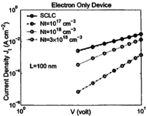
First, we consider the current–voltage relation with traps. In Fig. 1, current–voltage relation is plotted with trap densities Nt= 1017, 1018, and 3⫻1018cm−3, device thickness L = 100 nm, and0= 10−6cm2V−1s−1. In order to obtain the
inherent effect of traps on the field dependence of electron
mobility, we assume=0here. For comparison the
space-charge-limited current 共SCLC兲15 J =9
8⑀ V2
L3 共26兲
is also plotted. At low Nt, the current–voltage relation is
close to SCLC as expected. As Nt increases, electron traps
not only reduce the current, but also enhance the field
depen-FIG. 1. Current densities as a function of applied voltage are shown with
L = 100 nm. Electrons and holes have the same mobility of 10−6cm2V−1s−1.
The SCLC in Eq. 共26兲 is presented for comparison. Trap densities Nt
= 1017共dash兲, 1018共short dash兲, and 3⫻1018cm−3共dash dot兲 are considered.
dence of electron current. The electron current approaches SCLC more as the voltage increases. The reduced magnitude and stronger field dependence of the electron current have been described alternatively by a model with an effective electron mobility but no traps.6,7The effective mobility is of
the Poole–Frenkel form 关Eq. 共15兲兴 with artificially reduced
E0共stronger field dependence兲 and lower zero-field mobility 0 in order to describe the effect of traps. Below such
de-scription is named the asymmetry model, because the sym-metry between the electron and hole mobility is explicitly
broken. In Fig. 2共d兲 we show that the phenomenological
asymmetric model and our more microscopic trap model are
able to give the same current–voltage共I–V兲 curve. One then
wonders whether they give the same electron distribution or not. Figure 2 plots the electron distributions calculated using different models. The free-electron distributions in Fig. 2共a兲 are obtained from the trap model with Nt= 1018cm−3. The trapped electron distributions are presented in Fig. 2共b兲 with various applied voltages. The free-electron distributions cal-culated without traps in the asymmetric model are shown in Fig. 2共c兲. The hole mobility is as before, but the electron
mobility 0= 8⫻10−11cm2V−1s−1 and E0= 1.9
⫻104V cm−1are chosen to give the same I – V relation. The
free-electron density calculated in the trap model is much smaller than that in the asymmetry model, especially near the cathode. The smaller free-carrier density in the trap model is due to the fact that free electrons are much more mobile than those in the asymmetry model. Therefore, for a given current density much fewer electrons are needed to carry the current. This indicates that although the I – V curve can be fitted very well using the asymmetry model, the carrier density pre-dicted by such a model is incorrect. The free-electron density distribution is important for the exciton formation and quenching in bipolar devices. This suggests that any model without explicit inclusion of traps cannot be applied to the recombination and efficiency of PLED.
Next, we consider the effect of the traps on the transient time. The transient time is the real time that the device takes
to converge to the steady state in the time evolution. Figure 3 plots the transient time versus trap density at various volt-ages. 0is 10−6cm2V−1s−1, E
0is 5⫻105V cm−1, and L is
100 nm. As the trap density Ntincreases, the electrons need more time to fill up the traps, then go throughout the device. A smaller applied voltage also causes a longer transient time because of fewer electrons to fill up the traps. As the trap density become comparable to the free-electron density, the device slows down significantly. This happens when
nt= Nt
冉
nf n0冊
T/Tt ⯝nf0 10, 共27兲where nf0is free-electron density in the device with zero trap density.
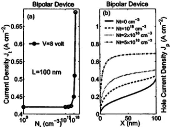
B. Bipolar device with traps
MEH-PPV is taken as the active layer sandwiched be-tween the Ca and Au electrode. Au, on the right-hand side of the device, has a 0.2-eV barrier for hole injection to MEH-PPV, and the thickness of the device L is 100 nm. n0,⑀r, T, and Tt are the same as those in the electron-only device.
Figure 4共a兲 plots the total current density as a function of the trap density Nt at 8 V. Here, 0= 10−6cm2V−1s−1 and
E0= 105V cm−1. The striking feature is that the current
in-FIG. 2. 共a兲 The free-electron densities, calculated using the trap model
共0e=0h=0兲 with 0= 10−6cm2V−1s−1, Nt= 1018cm−3, and E0
= 105V cm−1, are plotted.共b兲 The trapped electron densities calculated using
parameters as those in共a兲. 共c兲 The free-electron densities, calculated using the asymmetric model共0e⫽0h兲 with0e= 8⫻10−11cm2V−1s−1and E0e
= 1.9⫻104V cm−1, are presented.共d兲 The current densities calculated using
the asymmetric model共line兲 and trap model 共circle兲 from 2 to 10 V.
FIG. 3. The transient time with applied voltages 2, 4, 6, and 8 V is plotted against the trap density Nt. The thickness L is 100 nm. 0
= 10−6cm2V−1s−1and E
0= 5⫻105V cm−1.
FIG. 4. 共a兲 The current density vs trap density Ntfor a bipolar device is
presented with an applied voltage of 8 V. 0= 10−6cm2V−1s−1, E0
= 105V cm−1, and L = 100 nm.共b兲 The hole current density distributions are
plotted with trap densities 0, 1018, 2⫻1018, and 5⫻1018cm−3. The hole
injection at the anode共x=100 nm兲 increases with trap density.
114502-4 M. Tsai and H. Meng J. Appl. Phys. 97, 114502共2005兲
creases with Nt, contrary to what intuition would suggest. In electron-only devices, some electrons are trapped so that the electron current declines when the trap density Ntincreases. In bipolar devices, however, the trapped electrons increase the total negative space charge, which enhances the hole in-jection by Coulomb attraction, as illustrated in Fig. 4共b兲. The hole current density Jppresented in Fig. 4共b兲 increases with the trap density, causing a larger total current density.
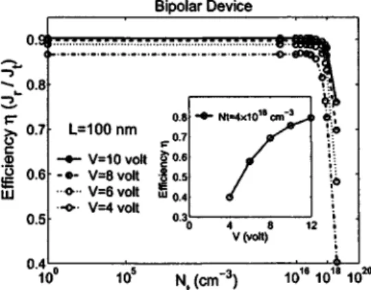
The PLED efficiencyis shown in Fig. 5 as a function
of the trap density Ntand the applied voltage. When Nt in-creases, the efficiency declines faster at a smaller voltage than that at a higher voltage, suggesting that the imbalance between the electron and hole current in the device with a smaller voltage exceeds that in the device at a higher voltage. This is consistent with Fig. 1, where IV approaches SCLC with increasing voltage. There are also critical trap densities in Fig. 5, determined by Eq.共27兲 as before. For fixed Nt, the efficiency of the device increases with the applied voltage since the traps are more filled up and the electron-hole injec-tion is more balanced, as shown in the inset.
The distribution of the recombination R is important in PLED, since the dominant light-generation zone determines how serious the cathode quenching effect is. Figure 6 plots the recombination distribution through the device. The re-combination distribution is symmetrical when Nt= 0, and the
main recombination zone approaches the cathode as Nt
creases. Also, the absolute value of recombination itself in-creases with the trap density near the cathode due to the increased density of holes, attracted toward the cathode by the trapped negative space charge. Clearly, the electron traps detrimentally affect the luminescence efficiency, since most excitons are quenched by the cathode plasma mode. Figure 7
plots the distribution of the recombination rate R with Nt
= 1018cm−3at various voltages. The figure shows that
apply-ing a higher voltage pushes the electrons away from the cath-ode to the ancath-ode, smoothing the distribution and reducing the cathode quenching. So at higher voltage, not only is the car-rier injection more balanced, as shown in Fig. 5, but also the cathode quenching is reduced. Both factors contribute to the increasing efficiency with voltage.
The transient time for the bipolar device is shown in Fig. 8. The device at high voltage needs less time to reach the steady state because the traps are filled rapidly as the picture in the electron-only device. For a lower voltage, the transient time could be as slow as a millisecond. Note that such a long transient time is not possible in the asymmetry model with-out traps.8 Because the build-in potential in the bipolar de-vice is larger than that in the electron-only dede-vice where electrons move faster, the transient time required for bipolar devices is longer than that for electron-only devices.
FIG. 5. The quantum efficiencyvs trap density Ntis presented in applied
voltages 4, 6, 8, and 10 V.0= 10−6cm2V−1s−1, E0= 5⫻105V cm−1, and
device thickness L = 100 nm. The inset shows the relation between efficiency and applied voltage.
FIG. 6. The distributions of recombination rate are plotted at 8 V. The recombination rate is shown for Nt= 0, 1017, 1018, and 3⫻1018cm−3. 0
= 10−6cm2V−1s−1and E
0= 105V cm−1.
FIG. 7. The distributions of recombination rate are presented with applied voltages 3, 6, 9, and 12 V. The trap density of 1018cm−3 is used.
0
= 10−6cm2V−1s−1and E
0= 105V cm−1.
FIG. 8. The transient time of a bipolar device vs trap density is shown. Here,0= 10−6cm2V−1s−1and E0= 5⫻105V cm−1. The device thickness is L = 100 nm.
Electron traps are inevitable as discussed in the Introduc-tion. After showing their adverse effect on the PLED effi-ciency, one may wonder if such an effect can be cured. One
promising idea is to introduce hole traps into the
semiconductor.23The hole traps are supposed to balance the carrier injection and increase the luminescent efficiency. Fig-ure 9共a兲 presents the efficiency for a device with an electron trap density of Nt= 5⫻1018cm−3 at 4 V. As the hole trap
density Pt is zero, = 0.35 due to the imbalance. As Pt in-creases, the efficiency is indeed enhanced and doubled from 0.35 to 0.7 when Pt= 5⫻1018cm−3, where the recombination distribution is symmetrical. Increasing the number of hole traps beyond the electron trap density 共Pt= 7⫻1018cm−3兲 diminishes the efficiency of the device, since the imbalance of carriers comes back. Hole traps also contribute to the fall in quenching, since the recombination rate is made smoother, as shown in Fig. 9共b兲.
C. Bilayer device
One of the most remarkable effects of the traps on the recombination distribution is that the recombination concen-trates near the cathode at low voltage and spreads out to the
whole device at higher voltage 共Fig. 7兲. Although such a
spread in recombination does not change the emission spec-trum for single-layer PLED, it suggests the possibility of
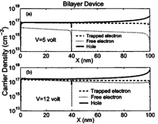
continuous color tuning by voltage in PLED with two emis-sive layers. Below we study a bilayer device with electron traps. In our device a green emissive layer next to the
cath-ode has a conduction-band energy Ec of 2.7 eV and a
valence-band energy Ev of 5.3 eV, with a thickness of
40 nm. The layer next to the anode is the red-emissive MEH-PPV, with a thickness of 60 nm. The device is sandwiched between Ca and Au electrodes, and the electron trap density
in each layer is 1018cm−3;
0= 10−6cm2V−1s−1, E0= 5 ⫻105V cm−1, n
0= 1021cm−3, and T and Tt are 300 and 1500 K. Figure 10 schematically depicts the bilayer device. Figure 11 shows the carrier densities of holes, free electrons, and trapped electrons at 5 V in the upper panel and 12 V in the lower panel. The shape of the hole distribution is quite uniform and does not depend on the voltage much. On the other hand, the electron density concentrates in the green layer at 5 V and becomes uniform at 12 V. The recombina-tion rate is shown in Fig. 12 at 5 and 12 V. As expected, the recombination in the red layer relative to the green layer increases significantly with voltage, resulting in a color tun-ing.
IV. CONCLUSION
Many experiments have demonstrated the imbalance of holes and electrons. We show here that all the observed re-sults can be captured by the electron trap model with
sym-FIG. 10. The scheme of a bilayer device is shown. Layer thicknesses and band energies are indicated.
FIG. 11. The carrier density distribution of holes, free electrons, and trapped electrons are shown in the bilayer device 共Fig. 10兲 at 5 and 12 V. 0
= 10−6cm2V−1s−1and E
0= 5⫻105V cm−1.
FIG. 9. 共a兲 Efficiency vs hole trap density is shown for the electron trap density Nt= 5⫻1018cm−3at 4 V. The hole trap densities Ptare 0, 1015, 5 ⫻1018, and 7⫻1018cm−3.
0= 10−6cm2V−1s−1and E0= 105V cm−1.共b兲
The recombination rate vs position is presented with the same parameters. The recombination is symmetrical when the hole and electron trap densities are the same, corresponding to a maximum value of the efficiency.
FIG. 12. Recombination rate vs position is shown with the applied voltage of 5 V in共a兲 and 12 V in 共b兲. Parameters are the same as that in Fig. 11.
114502-6 M. Tsai and H. Meng J. Appl. Phys. 97, 114502共2005兲
metric free-carrier mobilities. Although the asymmetry model, in which the imbalance is described by artificially breaking the mobility symmetry, can fit the current–voltage curve accurately, the predicted electron density significantly exceeds that calculated in the more microscopic trap model. The model without explicit consideration of traps is therefore inappropriate for discussing the device recombination rate or efficiency. Traps affect not only the current and recombina-tion, but also the transient time required for the device to reach the steady state. A time scale of millisecond arises in bipolar devices with higher trap density. In PLED, traps cause the recombination zone to approach the cathode, seri-ously affecting the device luminescence and efficiency due to the metal quenching. Addition of hole traps recovers the bal-ance of carrier densities and doubles the efficiency. Our works show that almost all transport and electrolumines-cence properties of organic devices are determined by the electron traps, and the control of such traps is the key to improve the PLED efficiency.
ACKNOWLEDGMENTS
This work was supported by the National Science Coun-cil of the Republic of China under Grant No. NSC89-2112-M009-047 and the Excellence Project Semiconducting Poly-mers for Electroluminescence under Grant No. 91-E-FAO4-2-4A of the ROC Ministry of Education.
1
J. H. Burroughes, D. D. C. Bradley, A. R. Brown, R. N. Marks, K. Mackey, R. H. Friend, P. L. Burn, and A. B. Holmes, Nature共London兲
347, 539共1990兲. 2
H. Antoniades, M. A. Abkowitz, and B. R. Hsieh, Appl. Phys. Lett. 65,
2030共1994兲.
3
P. W. M. Blom and M. C. J. M. Vissenberg, Mater. Sci. Eng., R. 27, 53
共2000兲.
4
L. Bozano, S. A. Carter, J. C. Scott, G. G. Malliaras, and P. J. Brock, Appl. Phys. Lett. 74, 1132共1999兲.
5
H. F. Meng and Y. S. Chen, Phys. Rev. B 70, 115208共2004兲.
6
B. K. Crone, P. S. Davids, I. H. Campbell, and D. L. Smith, J. Appl. Phys.
84, 833共1998兲. 7
P. S. Davids, I. H. Campbell, and D. L. Smith, J. Appl. Phys. 82, 12
共1997兲.
8
D. J. Pinner, R. H. Friend, and N. Tessler, J. Appl. Phys. 86, 5116共1999兲.
9
B. Ruhstaller, S. A. Carter, S. Barth, H. Riel, W. Riess, and J. C. Scott, J. Appl. Phys. 89, 4575共2001兲.
10
P. W. M. Blom and M. J. M. de Jong, IEEE J. Sel. Top. Quantum Electron.
4, 105共1998兲. 11
C. D. J. Blades and A. B. Walker, Synth. Met. 111–112, 335共2000兲.
12
A. J. Campbell, D. D. C. Bradley, and D. G. Lidzey, J. Appl. Phys. 82, 6326共1997兲.
13
P. E. Burrows, Z. Shen, V. Bulovic, D. M. McCarty, S. R. Forrest, J. A. Cronin, and M. E. Thompson, J. Appl. Phys. 79, 7991共1996兲.
14
K. C. Kao and W. Hwang, Electrical Transport in Solids共Pergamon, Ox-ford, 1981兲.
15
M. A. Lampert and P. Mark, Current Injection in Solids共Academic, New York, 1970兲.
16
P. W. M. Blom, M. J. M. de Jong, and S. Breekijk, Appl. Phys. Lett. 71, 930共1997兲.
17
V. N. Abadumov, V. I. Perel, and I. N. Yassievich, Nonradiative
Recom-bination in Semiconductors共North-Holland, Amsterdam, 1991兲, p. 10. 18
D. L. Scharfetter and H. K. Gummel, IEEE Trans. Electron Devices
ED-16, 64共1969兲. 19
H. Bässler, Phys. Status Solidi B 175, 15共1993兲.
20
Y. N. Gartstein and E. M. Conwell, Chem. Phys. Lett. 245, 351共1995兲.
21
D. H. Dunlap, P. E. Parris, and V. M. Kenkre, Phys. Rev. Lett. 77, 542
共1996兲.
22
B. K. Crone, P. S. Davids, I. H. Campbell, and D. L. Smith, J. Appl. Phys.
87, 1974共2000兲. 23
A. J. Campell, D. D. C. Bradley, T. Virgili, D. G. Lidzey, and H. Anto-niadis, Appl. Phys. Lett. 79, 3872共2001兲.