treatments
C. C. Lee, C. P. Lee, M. H. Yeh, W. I. Lee, and C. T. Kuo
Citation: Journal of Vacuum Science & Technology B 21, 1501 (2003); doi: 10.1116/1.1596217 View online: http://dx.doi.org/10.1116/1.1596217
View Table of Contents: http://scitation.aip.org/content/avs/journal/jvstb/21/4?ver=pdfcov Published by the AVS: Science & Technology of Materials, Interfaces, and Processing
Articles you may be interested in
Low-resistance, highly transparent, and thermally stable Ti/ITO Ohmic contacts to n - Ga N J. Vac. Sci. Technol. B 27, 1161 (2009); 10.1116/1.3136922
Effects of plasma treatment on the Ohmic characteristics of Ti Al Ti Au contacts to n -AlGaN Appl. Phys. Lett. 89, 082109 (2006); 10.1063/1.2338434
Low-resistance Ohmic contacts for high-power GaN field-effect transistors obtained by selective area growth using plasma-assisted molecular beam epitaxy
Appl. Phys. Lett. 89, 042101 (2006); 10.1063/1.2234566
Thermally stable, oxidation resistant capping technology for Ti/Al ohmic contacts to n-GaN J. Appl. Phys. 92, 4283 (2002); 10.1063/1.1507809
Low resistance ohmic contacts to n-GaN and n-AlGaN using NiAl Appl. Phys. Lett. 77, 382 (2000); 10.1063/1.126983
ambient treatments
*
C. C. Lee and C. P. Leea)
Department of Electronics Engineering, National Chiao Tung University, Hsinchu, Taiwan, Republic of China
M. H. Yeh and W. I. Lee
Department of Electrophysics, National Chiao Tung University, Hsinchu, Taiwan, Republic of China C. T. Kuo
Advanced Epitaxy Technology, Inc., Hsinchu Industrial Park, Taiwan, Republic of China
共Received 6 January 2003; accepted 9 June 2003; published 24 July 2003兲
In this article, a scheme for fabricating low resistance Ohmic contacts to n-GaN was developed. This approach takes advantage of Ar plasma treatment and thermal annealing in forming gas ambient. As a result, the adjustment of Ar flow rate was very effective in improving the contact resistance. After proper Ar plasma treatment, the contact resistance and specific contact resistance of as-deposited Ohmic contacts were reduced to 0.362⍀ mm and 3.9⫻10⫺5 ⍀ cm2, respectively. Low contact resistance共0.103 ⍀ mm兲 and specific contact resistance (3.2⫻10⫺6⍀ cm2) were obtained after annealing in N2 gas ambient. By performing thermal annealing in forming gas ambient, even lower contact resistance 共0.093 ⍀ mm兲 and specific contact resistance (2.6⫻10⫺6 ⍀ cm2) were successfully achieved, indicating that the electrical characteristics of Ohmic contacts would not be affected by the effect of hydrogen passivation of dopants in n-GaN. © 2003 American Vacuum
Society. 关DOI: 10.1116/1.1596217兴
I. INTRODUCTION
Nitride-based electronic devices, such as heterostructure field effect transistors, and heterojunction bipolar transistors, are potentially very useful for high power and high tempera-ture applications. To use these devices for such applications, good Ohmic contacts with low contact resistance are very important. In general, Ohmic contacts to n-GaN with low contact resistance are not easily obtainable because of its wide band gap. The improvement of contact resistance could be achieved by many approaches, such as the selection of the right contact metal,1–7 surface treatments,8,9 and plasma treatments.10–16 In addition, thermal annealing is also very important. Thermal annealing in N2gas ambient was usually employed to obtain low resistance Ohmic contacts. The main reason for using nitrogen gas as the annealing ambient in-stead of hydrogen containing gas, as commonly used by most III–V compounds, is to avoid the effect of hydrogen passivation of dopants in GaN.5,22In this work, a scheme of combining Ar plasma treatment and annealing in forming gas ambient for fabricating low resistance Ohmic contacts to
n-GaN was developed. We found that this approach could
further improve the contact resistance. With appropriate Ar plasma treatment, the contact resistances of the as-deposited Ohmic contacts were improved substantially. Moreover, after subsequent annealing in the forming gas ambient, contacts treated with this scheme have even lower contact resistance than those annealed in N2 gas ambient. This indicates that
the electrical characteristics of Ohmic contacts would not be affected by the effect of hydrogen passivation of dopants in
n-GaN.
II. EXPERIMENT
The 2-m-thick n-GaN films for this study were grown by metalorganic chemical vapor deposition on c-plane sap-phire substrates. The electron concentration and the mobility obtained by Hall measurement were 3.3⫻1018cm⫺3 and 248 cm2/V s, respectively. After layer growth, mesa patterns for transmission line measurement 共TLM兲 were defined by photolithography. Prior to contact metal deposition, the samples were treated by different Ar plasma conditions using inductive coupled plasma 共ICP兲 system and then dipped in the solution of 1:1 HCl:H2O for 1 min. Contact metal, Ti/Al/ Ti/Au 共200/1500/450/550 Å兲, was then deposited and lifted off to form the contact pads. The dimension of contact pad was 110⫻110m2. The samples were annealed at 750 °C for 30 s in N2 or forming gas ambient. After annealing, the TLM measurement was performed for the determination of the contact resistance.
III. RESULTS AND DISCUSSION
The conditions of the plasma treatment are shown in Table I. It should be noted that a very low bias power of 5 W was used in the plasma treatment to ensure a very slow etch-ing rate for GaN. Only about 100–200 Å was etched duretch-ing the plasma treatment. Figure 1 shows the current–voltage characteristics of the as-deposited Ohmic contacts under dif-ferent Ar flow rate. With the increase of Ar flow, the current– voltage characteristics of these contacts became more linear.
*No proof corrections received from author prior to publication.
Figure 2 shows the dependence of the contact resistance and the specific contact resistance as functions on the Ar flow rate. Both the contact resistance and specific contact resis-tance decreased as the Ar flow rate was increased. For samples without Ar plasma treatment, the contact resistance and the specific contact resistance were too high to be ex-tracted via TLM measurement. Samples treated with an Ar flow rate of 50 sccm showed the best result. Their contact resistance and specific contact resistance were 0.362 ⍀ mm and 3.9⫻10⫺5⍀ cm2, respectively. After annealing, all samples showed linear current–voltage characteristics, as shown in Fig. 3. Similar dependences of the contact resis-tance and the specific contact resisresis-tance of the alloyed con-tacts on Ar flow rate were obtained as well, as shown in Fig. 4. All alloyed contacts have low contact resistances. Samples treated with 50 sccm of Ar flow rate still exhibited the best electrical characteristics. Their contact resistance and spe-cific contact resistance were 0.103 ⍀ mm and 3.2 ⫻10⫺6 ⍀ cm2, respectively.
Apparently, the Ar flow rate has a significant influence on contact resistance. With the increase of Ar flow rate, the
con-FIG. 1. Current–voltage characteristics of the as-deposited Ohmic contacts
treated with Ar plasma at different Ar flow rates.
FIG. 2. Dependence of contact resistance and specific contact resistance of
the as-deposited Ohmic contacts on Ar flow rate.
TABLEI. Conditions of the plasma treatment.
ICP power共W兲 ¯ 300 300 300 300 300
Bias power共W兲 ¯ 5 5 5 5 5
Pressure共mTorr兲 ¯ 15 15 15 15 15
Ar flow共sccm兲 ¯ 10 30 50 50 50
Time共min兲 ¯ 1 1 1 2 3
FIG. 3. Current–voltage characteristics of the alloyed Ohmic contacts under
different Ar flow rates.
FIG. 4. Dependence of contact resistance and specific contact resistance of
the alloyed Ohmic contacts on Ar flow rate.
tact resistance is improved greatly. The mechanism of Ar plasma etching is physical ion bombardment. Higher Ar flow rate generates higher Ar ion density in the plasma, which enhances the effect of ion bombardment on wafer surface. Thus, more lattice damage and crystalline defects are created on the wafer surface. The increase of nitrogen vacancies on the wafer surface after plasma treatment has been shown by many researchers10,13,15and they are generally believed to be native donors.17,18Therefore, after plasma treatment with Ar, the improvement of contact resistance is due to the increase of nitrogen vacancies on the wafer surface.
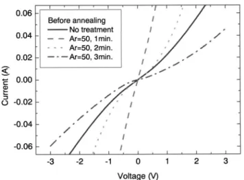
Figure 5 shows the current–voltage characteristics of the as-deposited Ohmic contacts共before annealing兲 with differ-ent Ar treatmdiffer-ent time. We found that Ar treatmdiffer-ent improves the Ohmic contact if the duration is less than 1 min. But, if it is too long, the Ohmic contact becomes worse. After a 3 min of Ar plasma treatment, the current–voltage characteristics are even poorer than those without treatment. After thermal annealing, all samples show good Ohmic behavior, as shown in Fig. 6. Substantial improvement can be obtained for the
samples treated with shorter times (t⫽1, 2 min兲. Figure 7 shows the dependence of contact resistance and specific con-tact resistance of the alloyed concon-tacts on the treatment time. As a whole, samples with different treatment times all have lower contact resistances and specific contact resistances than those without treatment. However, for the best result, the treatment time has to be kept no longer than 1 min. The samples with 1 min of Ar plasma treatment have the lowest contact resistance 共0.103 ⍀ mm兲 and specific contact resis-tance (3.2⫻10⫺6⍀ cm2).
Plasma treatment not only produces nitrogen vacancies on the surface, which is desirable for the improvement of con-tact resistance, but also causes crystalline defects, which can degrade the film quality and the contact resistance.12 So, to use such a technique for contact improvement, one has to carefully choose the treatment time so that the damage it causes does not overwhelm the benefit it produces.
Figure 8 shows the current–voltage characteristics of the Ohmic contacts after annealing in forming gas共15% H2). All samples showed good Ohmic behavior. In comparison with the samples without plasma treatment, substantial
improve-FIG. 5. Current–voltage characteristics of the as-deposited Ohmic contacts
under different Ar treatment times.
FIG. 6. Current–voltage characteristics of the alloyed Ohmic contacts under
different Ar treatment times.
FIG. 7. Dependence of contact resistance and specific contact resistance of
the alloyed Ohmic contacts on Ar treatment time.
FIG. 8. Current–voltage characteristics of the Ohmic contacts annealed in
ment in electrical characteristics was obtained as well. Figure 9 shows the comparison of specific contact resistance of the Ohmic contacts annealed in N2 and in forming gas ambient. Similar to the results of those annealed in N2gas, the specific contact resistance of the samples annealed in forming gas decreases with the Ar flow rate. It is apparent that the form-ing gas treated contacts have lower specific contact resis-tance than those annealed in N2 gas ambient. The lowest contact resistance and specific contact resistance obtained here are 0.093⍀ mm and 2.6⫻10⫺6⍀ cm2, respectively.
Obviously, from the results presented above, annealing in forming gas is better than annealing in N2. The possible reason is the reduction capability of the forming gas because of the H2 content. It may reduce the oxidation reaction of metal at high temperatures and, therefore, help reduce the contact resistance. Similar results were also observed in the Al/n-GaN Ohmic contacts annealed in Ar/4% H2 forming gas.19The H2 content, however, may cause concerns in dop-ing reduction because of hydrogen passivation. It is known that hydrogen passivation of p-type dopants in p-GaN would result in a large decrease of hole concentration.20,21Whether annealing in forming gas ambient would lead to a similar reduction in electron concentration and increase of contact resistance of n-GaN needs to be answered. During the an-nealing process, H2 could diffuse into the bulk n-GaN to form neutral complexes with dopants at annealing tempera-ture higher than 500 °C. On the other hand, the high tem-perature annealing process would also result in the dissocia-tion of neutral dopant-H complexes.22Although the effect of hydrogen passivation of n-type dopants in n-GaN during the annealing and subsequent cooling process is not completely known, the results obtained here indicate that annealing in forming gas ambient would not lead to electrical degradation of Ohmic contacts.
IV. CONCLUSION
Ar flow rate can have a significant effect on contact resis-tance for Ohmic contacts to n-GaN. With the increase of Ar
flow rate, the contact resistance of plasma-treated Ohmic contacts to n-GaN was greatly improved. Longer plasma treatment time does not necessarily improve the contact re-sistance of contacts. Therefore, proper control over plasma damage is required for the greatest improvement of contact resistance. Lower contact resistance and specific contact re-sistance were obtained for contacts annealed in forming gas ambient than those annealed in N2 ambient. This indicates that the electrical characteristics of Ohmic contacts would not be influenced by the effect of hydrogen passivation of dopants in n-GaN. With such a combination of appropriate Ar plasma treatment and annealing in forming gas ambient, low resistance Ohmic contacts to n-GaN were obtained.
ACKNOWLEDGMENTS
This work was supported by the National Science Council under Contract No. 90-2215-E-009-013. The authors would like to acknowledge the assistance of the National Nano De-vice Laboratory. The authors also appreciate the support of Dr. C. F. Lin, Semiconductor Research Center, National Chiao Tung University.
1J. S. Foresi and T. D. Moustakas, Appl. Phys. Lett. 62, 2859共1993兲.
2M. E. Lin, Z. Ma, F. Y. Huang, Z. F. Fan, L. H. Allen, and H. Morkoc,
Appl. Phys. Lett. 64, 1003共1994兲.
3
M. W. Cole, D. W. Eckart, W. Y. Han, R. L. Pfeffer, T. Monahan, F. Ren, C. Yuan, R. A. Stall, S. J. Pearton, Y. Li, and Y. Lu, J. Appl. Phys. 80, 278
共1996兲.
4J. H. Chern, L. P. Sadwick, and P. J. Hwu, Proceedings of the High
Temperature Electronics Conference共1998兲, p. 114.
5
Q. Z. Liu and S. S. Lau, Solid-State Electron. 42, 677共1998兲.
6L. L. Smith, R. F. Davis, R. J. Liu, M. J. Kim, and R. W. Carpenter, J.
Mater. Res. 14, 1032共1999兲.
7C. T. Lee and H. W. Kao, Appl. Phys. Lett. 76, 2364共2000兲.
8
Y. Koyama, T. Hashizume, and H. Hasegawa, Solid-State Electron. 43, 1483共1999兲.
9Y. J. Lin and C. T. Lee, Appl. Phys. Lett. 77, 3986共2000兲.
10Z. Fan, S. N. Mohammad, W. Kim, O. Aktas, A. E. Botchkarev, and H.
Morkoc, Appl. Phys. Lett. 68, 1672共1996兲.
11
H. S. Kim, Y. H. Lee, G. Y. Yeom, J. W. Lee, and T. I. Kim, Mater. Sci.
Eng., B 50, 82共1997兲.
12A. T. Ping, Q. Chen, J. W. Yang, M. Asif Khan, and I. Adesida, J.
Elec-tron. Mater. 27, 261共1998兲.
13
J. Y. Chen, C. J. Pan, and G. C. Ghi, Solid-State Electron. 43, 649共1999兲.
14C. R. Eddy, Jr., and B. Molnar, J. Electron. Mater. 28, 314共1999兲.
15J. M. Lee, K. M. Chang, S. W. Kim, C. Huh, I. H. Lee, and S. J. Park, J.
Appl. Phys. 87, 7667共2000兲.
16H. W. Jang, C. M. Jeon, J. K. Kim, and J. L. Lee, Appl. Phys. Lett. 78,
2015共2001兲.
17H. P. Maruska and J. J. Tieyjen, Appl. Phys. Lett. 15, 327共1969兲.
18R. J. Molnar, T. Lei, and T. D. Moustakas, Appl. Phys. Lett. 62, 72
共1993兲.
19
B. P. Luther, S. E. Mohney, T. N. Kackson, M. A. Khan, Q. Chen, and J.
W. Wang, Appl. Phys. Lett. 70, 57共1997兲.
20S. Nakamura, T. Mukai, M. Senoh, and N. Iwasa, Jpn. J. Appl. Phys., Part
2 31, L139共1992兲.
21S. Nakamura, N. Iwasa, M. Senoh, and T. Mukai, Jpn. J. Appl. Phys., Part
1 31, 1258共1992兲.
22S. J. Pearton, J. C. Zolper, R. J. Shul, and F. Ren, J. Appl. Phys. 86, 1
共1999兲.
FIG. 9. Comparison of specific contact resistance of the Ohmic contacts
annealed in N2gas and in forming gas ambient.