國 立 交 通 大 學
電子工程學系 電子研究所
博 士 論 文
前瞻非揮發性奈米晶體記憶體元件之
製作與特性研究
Fabrication and Characterization of
Advanced Nonvolatile Nanocrystals Memory
研 究 生 :楊 富 明
指導教授 :羅 正 忠 博 士
張 鼎 張 博 士
前瞻非揮發性奈米晶體記憶體元件之
製作與特性研究
Fabrication and Characterization of
Advanced Nonvolatile Nanocrystals Memory
研 究 生 :楊 富 明
Student: Fu-Ming Yang
指導教授 :羅 正 忠 博 士
Advisor: Dr. Jen-Chung Lou
張 鼎 張 博 士 Dr. Ting-Chang Chang
國 立 交 通 大 學
電子工程學系 電子研究所
博 士 論 文
A Dissertation
Submitted to Department of Electronics Engineering and Institute of Electronics
College of Electrical and Computer Engineering National Chiao Tung University
in partial Fulfillment of the Requirements for the Degree of
Doctor of Philosophy in
Electronics Engineering November 2007
Hsinchu, Taiwan, Republic of China
推 薦 函
事由: 推薦電子研究所博士班研究生楊富明提出論文,參加國立交
通大學博士論文口試。
說明: 本校電子研究所博士班研究生楊富明,業已修畢部訂所需課
程學分,通過博士資格考之學科考試,並完成博士論文「前
瞻非揮發性奈米晶體記憶體元件之製作與特性研究」初稿,
且有數篇相關之論文發表或送審,茲列舉如下:
International Regular Journals
:
[1] F. M. Yang, T. C. Chang, P. T. Liu, C. W. Chen, Y. H. Tai, J. C. Lou, “Damage effect of fluorine implantation on PECVD α-SiOC barrier dielectric”, Nuclear Instrument and Methods in Physics Research. B, 237(1-2), p.301 (2005)
[2] F. M. Yang, T. C. Chang, Po-Tsun Liu, P. H Yeh, Y. C. Yu, J. Y. Lin, S. M. Sze, J. C. Lou, “Nickel silicide nanocrystals embedded in SiO2 and HfO2 for Nonvolatile
Memory Application”, accepted by Thin Solid Films (2007).
International Letter Journals
:
[1] F. M. Yang, T. C. Chang, Po-Tsun Liu, P. H Yeh, Y. C. Yu, J. Y. Lin, S. M. Sze, J. C. Lou, “Memory characteristics of Co nanocrystal memory device with HfO2 as
blocking oxide” Appl. Phys. Lett., 90, 132102(2007)
[2] F. M. Yang, T. C. Chang, Po-Tsun Liu, P. H Yeh, U. S. Chen, Y. C. Yu, J. Y. Lin, S. M. Sze, J. C. Lou, “Using double layer CoSi2 nanocrystals to improve the
memory effects of nonvolatile memory devices” Appl. Phys. Lett., 90, 212108(2007)
[3] F. M. Yang, T. C. Chang, Po-Tsun Liu, U. S. Chen, P. H Yeh, Y. C. Yu, J. Y. Lin, S. M. Sze , J. C. Lou, “Nickel nanocrystals with HfO2 blocking oxide for
綜上所陳,楊君已具備國立交通大學電子研究所應有之教育及訓練水
準,謹此推薦楊君參加交通大學電子研究所博士論文口試。
此致
國立交通大學電子研究所
電子研究所教授 羅正忠 博士
張鼎張 博士
中 華 民 國 九 十 六 年 8 月 13 日
前瞻非揮發性奈米晶體記憶體元件之
製作與特性研究
研究生:楊富明
指導教授: 羅正忠 博士
張鼎張 博士
國立交通大學
電子工程學系 電子研究所博士班
中文摘要 本論文主要是針對非揮發性奈米點記憶體元件做研究。我們成功的製作出用鈷 作為奈米點的結構。鈷奈米點包含在以二氧化矽以及二氧化鉿分別當作穿遂氧化 層和控制氧化層之間。通過電性分析,可以發現其具有明顯的記憶效應。在5伏 特的低操作電壓下,其記憶窗口(memory window)約為1伏特左右。同時,其保存 特性(retention characteristic)也相當驚人。而且,其忍耐度(endurance)在經過106 次的寫入/抹除之後,也沒有衰退。 同時,我們也成功製作出以鎳奈米點當作分離式電荷儲存點記憶體,埋在二 氧化矽以及二氧化鉿之間的結構。由穿遂式顯微鏡得知,鎳奈米點平均大小約為 5奈米以及密度約為3.9°1012 /cm2。鎳奈米點記憶體,在4伏特的寫入電壓操作的保存時間(retention time),極少的電荷流失率(charge loss rate)。此外,記
憶體的忍耐度即使到達106次的寫入/抹除之後,也不會衰退的現象出現。
此外,我們也成功的製作以矽化鈷當作奈米點的記憶體。矽化鈷奈米點,埋
在分別以二氧化矽以及二氧化鉿為穿遂氧化層和控制氧化層之間。其中我們以電
子繞射圖樣分析(electron diffraction pattern),確定奈米點為矽化鈷。矽化鈷奈米
點記憶體,在9伏特的電壓操作下有約為1.6伏特的切入電壓偏移。具有很長時間 的保存時間且很低的電荷流失率。忍耐度即使到達106次的寫入/抹除之後也沒有 變差。 同時,我們也成功製作出以矽化鎳奈米點在二氧化矽以及二氧化鉿之間的結 構。在電性方面的特性可以發現有很大的記憶窗口。在操作電壓為4伏特的低電 壓下,很明顯的得知有1.3伏特切入電壓偏移。這種的結構的製程將與現今半導 體業界的製程相符合。 最後,在論文中我們成功的製作出多層奈米點結構的記憶體。這種多層奈米 點的記憶體的優點將提高記憶體的效應。藉著增加奈米點的密度可增進保存時間 的特性。雙層的奈米點記憶體比起單層的記憶體有更多的電子儲存在裡面。雙層 的矽化鈷奈米點記憶體比單層的記憶體有更好的保存特性。然而,雙層結構的記 憶體之所以有較佳的保存特性是因為在上層的 Coulomb-blockage 效應,使得底 層的電子不易流失。所以,藉由雙層的奈米點可以有效增進奈米點記憶體的記憶 效應。
Fabrication and Characterization of Advanced
Nonvolatile Nanocrystals Memory
Student:
Fu-Ming
Yang
Advisors: Prof. Jen-Chung Lou
Prof.
Ting-Chang
Chang
Department of Electronics Engineering and Institute of Electronics
National Chiao Tung University, Hsinchu, Taiwan
Abstract
We have studied experimentally and theoretically nonvolatile nanocrystal memory
devices. On the study of nanocrystal memory, the Co nanocrystals using SiO2 and
HfO2 as the tunneling and the control dielectric with memory effect has been
fabricated. A significant memory effect was observed through the electrical
measurements. Under the low voltage operation of 5V, the memory window was
estimated to ~ 1V. The retention characteristics were tested to be robust. Also, the
endurance of the memory device was not degraded up to 106 write/erase cycles.
A distributed charge storage with Ni nanocrystals embedded in the SiO2 and
nonvolatile memory device with Ni nanocrystals exhibits 1 V threshold voltage shift
under 4 V write operation. The device has a long retention time with a small charge
lose rate. Besides, the endurance of the memory device is not degraded up to 106
write/erase cycles.
On the study of the CoSi nanocrystals with distributed charge storage elements
embedded between the SiO2 and HfO2 layer has been proposed. The nanocrystals
were identified to be CoSi phase by the analysis of electron diffraction pattern. The
nonvolatile memory device with CoSi nanocrystals exhibits 1.6 V threshold voltage
shift under 9 V write operation. The device has a long retention time with a small
charge lose rate. In addition, the endurance is not degraded up to 106 write/erase
cycles.
Also, a nonvolatile memory device with NiSi2 nanocrystals embedded in the
SiO2 and HfO2 layer has been fabricated. A significant memory effect is observed on
the characterization of the electrical properties. When a low operating voltage, 4V, is
applied, a significant threshold-voltage shift of 1.3V, is observed. The processing of
this structure is compatible with the current manufacturing technology of
semiconductor industry.
Finally, the nonvolatile memory device with multilayer nanocrystals has
the nanocrystals and the whole retention characteristic can be improved. There are
much more electrons that can be stored in the double layer than single layer
nanocrystal memory device. The double layer CoSi2 nanocrystals have better
retention characteristic than the single layer. The good retention characteristic of the
double layer device is due to the Coulomb-blockage effects on the top layer
nanocrystals from the bottom layer nanocrystals. So, the memory effects of the
誌 謝
能夠取得這個學位,我最感謝的是我的兩位指導教授,羅正忠教
授以及張鼎張教授。羅正忠教授溫文儒雅的氣質是我對老師的印象,
他不但教會我許多為人處事的態度和看法,還培養我獨自面對問題以
及解決問題的能力,盡信書不如無書,對於任何可疑的地方都必須要
挑戰他,也是我從老師平時的教導中領悟到的。張鼎張教授對於我的
研究方面的指導更是不遺餘力,在研究的過程當中碰到困難時,都會
給予適當協助,並排除問題,在平時老師也會很親切的關心學生的生
活以及近況,造就學長與學弟之間相處融洽的氣氛以及充滿歡笑聲的
環境,這些都是令我難以忘懷的。非常感謝兩位老師在我博士求學的
過程中,費盡心思教導我。
在此,我也要感謝交大顯示所劉柏村教授對我研究的方向以及論文
方面的指導,幫助我在論文寫作上更加的順利。特別感謝葉炳宏博
士,對於我研究上發生的問題,都會適時的提醒我,沒有他的話,就
沒有今天的我。感謝我的學長陳紀文博士,一路走過來沒有你的照應
以及幫助,我相信我現在的人生還是黑白的。蔡宗鳴博士,讓我肅然
起敬的學長,即使在你博士畢業前夕,都還會特地跑來教導沒有投稿
經驗的我如何投稿。同時,我也要感謝莫亦先博士以及顏碩廷博士關
心我的研究以及生活。
我感謝博士論文口試當天的口試委員:龔正教授、連振炘教授、張
國明教授、金雅琴教授、簡昭欣教授以及卓志臣博士。在您們的指導
下,才使得我的博士內容更加的充實。
同時,我也要感謝跟我在大學時就認識的好友:世青,一個值得信
賴的好伙伴;峻豪,從以前到現在無話不談的好朋友;世璋,遇到事
情不順利的時候,我都會想起你的咖啡;大山 ,一直到現在還是又
高又帥;敏全,感謝你在口試前一天的祝福;星舟,說話特別猛;致
宏學長,對於任何事情都有自己的堅持,感謝你們讓我在求學的過程
中不孤單;也謝謝我的室友世明學長,每晚都陪我去便利商店買宵夜。
在此,我也要感謝我的學弟,淵洲 ,在實驗上對我的配合,立偉、
緯仁、志瑋、勝凱、佳州、彥廷、睿龍、麗雯、仕承、志晟以及昭正
與你們相處的日子裡,充滿了歡樂。
在這過程中,我的女友珮婷小姐,一直陪伴我,感謝妳在我身邊,
當我失意時,總是背後默默的做我最佳的啦啦隊,謝謝妳。
士,雖然爸爸過世了,但是我認為您還在的話,一定會為了我而感到
驕傲,媽媽,妳一個人撐起這個家,讓我們這幾個無後顧之憂的完成
學業,並讓我順利的取得博士學位,我認為您也會以我為榮的,感謝
弟弟富昌以及妹妹淑華,讓我在遇到挫折時,給我適時的關心,謝謝
你們。
富明
2007 年 11 月于新竹交大
Contents
Chinese Abstract---
IEnglish Abstract---
IIIContent ---
VIAcknowledgment---
VIIITable Captions ---
XFigure Captions---
XIChapter 1 Introduction
1.1 General Background---11.2.SONOS nonvolatile memory devices ---2
1.3 Nanocrystals nonvolatile memory devices ---4
1.4 Organization of the dissertation --- 7
Chapter 2 Memory characteristics of Co nanocrystals memory device
with HfO
2as blocking oxide
2.1 Motivation--- ---142.2 Experimental procedures---
-
---152.3 Results and discussions--- ---16
2.4 Conclusions --- ---19
Chapter 3 Nickel nanocrystals with HfO
2blocking oxide for
nonvolatile memory application
3.1 Motivation ---283.2 Experimental procedures ---29
3.3 Results and discussions ---30
3.4 Conclusions ---32
3.5 Retention characteristics different with Co and Ni nanocrystals memory device ---32
Chapter 4 Fabrication and electrical characteristics of CoSi
nanocrystals nonvolatile memory with HfO
2blocking
oxide for memory device applications
4.1 Motivation ---434.2 Experimental procedures ---44
Chapter 5 Nickel silicide nanocrystals embedded in SiO
2and HfO
2for Nonvolatile Memory Application
5.1 Motivation ---52
5.2 Experimental procedures ---53
5.3 Results and discussions ---53
5.4 Conclusions ---56
Chapter 6 Using double layer CoSi
2nanocrystals to improve the
memory effects of nonvolatile memory devices
6.1 Motivation ---646.2 Experimental procedures ---65
6.3 Results and discussions ---66
6.4 Conclusions --- 68
Chapter 7 Comparison electric characteristics with metal and
metal-silicide nanocrystals memory device with HfO
2as
blocking oxide
7.1 Motivation ---747.2 Results and discussions ---74
Chapter 8 Conclusions and Suggestions for Future Work
8.1 Conclusions ---798.2 Suggestions for future work ---83
References
---84Vitae
---99Table Captions
Chapter 2
Table 2-1 AFM analysis of Co thin film(scan area: 5 × 5 μm ). ---
-
---21Chapter 3
Table 3-1 AFM analysis of Ni thin film. ---
-
----
---35Chapter 7
Table 7-1 The operation voltage of metal and metal-silicide nanocrystals memory
device dependence of memory window. ---
-
---77Table 7-2 The reliability characteristics of metal and metal-silicide nanocrystals
Figure Captions
Chapter 1
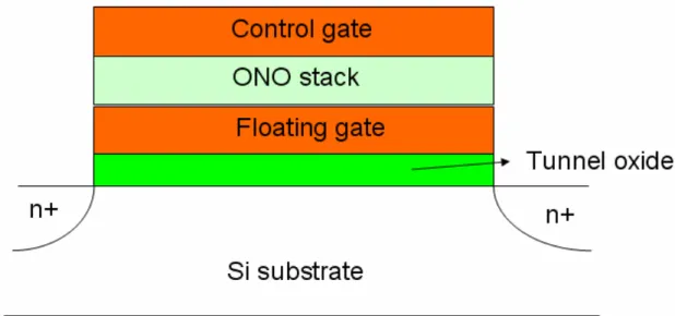
Fig.1-1 The structure of the conventional floating gate nonvolatile memory device.
Continuous poly-Si floating gate is used as the charge storage element and
ONO sandwiched structure is used as the control oxide---9
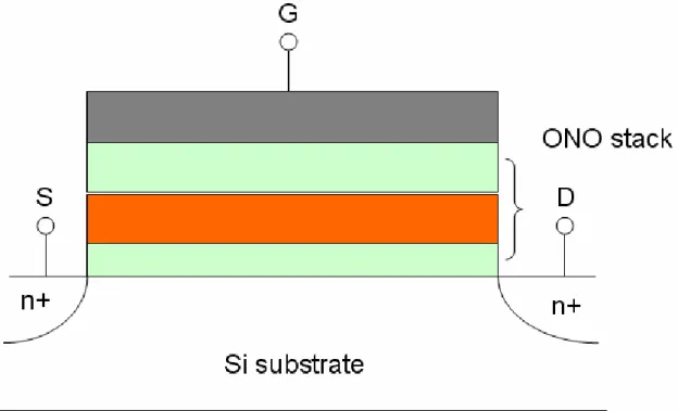
Fig.1-2 The structure of the SONOS nonvolatile memory device. The nitride layer
is used as the charge-trapping element---10
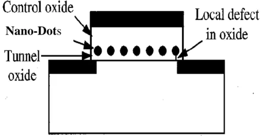
Fig.1-3 The structure of the nanocrystal nonvolatile memory device. The
semiconductor nanocrystals or metal nano-dots are used as the charge
storage element instead of the continuous poly-Si floating gate. ---11
Fig.1-4 The development of the gate stack of SONOS EEPROM memory devices.
The optimization of nitride and oxide films has been the main focus in
recent years. ---12
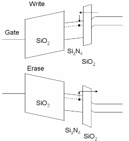
Fig.1-5 The energy band diagrams of the write/erase operation for a SONOS
device. ---13
Chapter 2
Fig.2-1 Process flow of an HfO2/Co/SiO2/Si stacked structure---20
structure. ---22
Fig.2-3 The capacitance-voltage (C-V) hysteresis of Co nanocrystals memory
device after bidirectional sweeps between 5V/(-5V) and 7V/(-7V). ---23
Fig.2-4 Gate voltage dependence of the memory window. ---24
Fig.2-5 The band diagrams of the operation of the distributed charge storage with
Co nano-dots. ---25
Fig.2-6 Data retention characteristics of the Co nanocrystals memory device. ----26
Fig.2-7 Endurance characteristics of the Co nanocrystals memory device. ---27
Chapter 3
Fig.3-1 Process flow of an HfO2/Co/SiO2/Si stacked structure---34
Fig.3-2 Cross-section TEM micrographs of an Ni/SiO2/Si stacked structure. ---36
Fig.3-3 The capacitance-voltage (C-V) hysteresis of Ni nanocrystals memory
device after bidirectional sweeps between 4V/(-4V) and 5V/(-5V). ---37
Fig. 3-4 Gate voltage dependence of the memory window. ---38
Fig.3-5 The retention characteristics of the Ni nanocrystals memory device at room
temperature. ---39
Fig.3-6 The endurance characteristics of the Ni nanocrystals memory device at
Fig. 3-7 Retention for Ni and Co nanocrystals nonvolatile memory. ---41
Fig. 3-8 Band diagram of Ni and Co nanocrystals nonvolatile memory. ---42
Chapter 4
Fig.4-1 The process flow proposed in this work. ---47
Fig.4-2 The electron diffraction pattern corresponding to CoSi nanocrystals.---48
Fig.4-3 The capacitance-voltage (C-V) hysteresis of CoSi nanocrystals memory
device after bidirectional sweeps between 9V/(-9V) and 12V/(-12V). The
inset is cross-section TEM micrographs of an HfO2/CoSi/SiO2/Si stacked
structure. ---49
Fig.4-4 Data retention characteristics of the CoSi nanocrystals memory device.--50
Fig.4-5 Endurance characteristics of the CoSi nanocrystals memory device.---51
Chapter 5
Fig.5-1 The process flow of nickel silicide nanocrystals. ---57
Fig.5-2 The capacitance-voltage (C-V) hysteresis of nickel silicide nanocrystals
memory device after bidirectional sweeps between 8V/(-8V) and
10V/(-10V). ---58
stacked structure. ---59
Fig.5-4 The electron diffraction pattern corresponding to nickel silicide nanocrystals.
---60
Fig.5-5 The capacitance-voltage (C-V) hysteresis of sample with α-Si/Ni/α-Si
structure after dry oxidation at 700℃. ---61
Fig.5-6 The capacitance-voltage (C-V) hysteresis of sample with α-Si/Ni/α-Si
structure after dry oxidation at 600℃. ---62
Fig.5-7 The memory window vs. (program/erase) voltage of nickel silicide
nanocrystal memory. ---63
Chapter 6
Fig.6-1 The capacitance-voltage (C-V) hysteresis of CoSi2 nanocrystals memory
device after bidirectional sweeps between 5V/(-5V) and 7V/(-7V). The
inset is cross-section TEM micrographs of an CoSi2 stacked structure. --69
Fig.6-2 The different memory effects of the single and double layer CoSi2
nanocrystals. ---70
Fig.6-3 Data retention characteristics of the CoSi2 nanocrystals memory device.
---71
---72
Fig.6-5 The band diagrams of “write” and “erase” operations of the double layer
nanocrystals with different gate polarities of the memory device. ---73
Chapter 7
Chapter 1
Introduction
1.1 General Background
Because of the high cost, large volume, and high power consumption of the
magnetic-core memory, the electronic industries wanted a new kind of memory device
to replace the magnetic-core memory. D. Kahng and S. M. Sze invented the
floating-gate (FG) nonvolatile semiconductor memory at Bell Labs in 1967 [1.1]. The
stacked-gate FG device structure, as shown in Fig. 1-1, continues to be the most
prevailing nonvolatile-memory implementation, and is widely used in both standalone
and embedded memories up to now. The invention of FG memory (flash memory)
creates a huge industry of portable electronic systems such as mp3 player, digital
cameras and USB flash personal disc etc.
Despite of a huge achievement for commercialization, conventional FG device
have some drawback. One of important issues is the limited potential for continued
scaling of the device structure. This scaling limitation focuses on the tunnel oxide
layer. The tunnel oxide has to allow quick and efficient charge transfer to and from the
FG. On the contrary, the tunnel oxide needs to provide superior isolation under
integrity over periods of up to a decade. If the tunnel oxide creates a leaky path, the
overall stored charge in the floating gate will be lost. When the tunnel oxide is thinner
for quick and efficient charge transformation on the FG, the retention characteristics
may be degraded.And when the tunnel oxide is made thicker to take the isolation into
account, the speed of the operation will be slower. Therefore, for mass production,
there is a trade-off between speed and reliability for the optimal tunnel oxide
thickness [1.2].
Two candidates are mostly used to overcome the scaling limits of the conventional
FG structure. One is SONOS memory devices [1.3-1.5] and the other is nanocrystal
nonvolatile memory devices [1.6-1.8]. Fig. 1-2 presents SONOS memory device. The
nitride layer is used as the charge-trapping element. The SONOS memory device
improved endurance since a single defect will not cause the discharge of the memory
[1.5]. Tiwari et al. [1.6] are the first time demonstration about the Si nanocrystal
floating gate memory device. In Fig. 1-3, the local leaky path of the nanocrystal
nonvolatile memory device will not cause the fatal loss of data. The nanocrystal
memory device can not only maintain good retention characteristics when tunnel
oxide is thinner but also lower the power consumption [1.6-1.8]. These structures can
prevent the stored charges out of from charge trapping elements.
The nonvolatile memory devices should withstand (about 106) cycles and ten years
at high temperature. In general, the program/erase cycles is called endurance. The
term “endurance” means ability of the NVSM to withstand repeated program/erase
cycles and still maintain the data in the NVSM. The term “retention” shows the ability
of the NVSM to store and recover information after a number of program/erase cycles
at a specified temperature. Figure 1-4 illustrates the SONOS device structure
progression of device cross section. The first metal-gate nitride device
metal/nitride/oxide/silicon (MNOS) was reported in 1967 by Wegener et al [1.9]. In
the early 1970s, the initial device structures were p-channel
metal-nitride-oxide-silicon (MNOS) structures which with Al gate electrodes and 45
nm silicon nitride as charge storage layers. Program/erase voltages of devices were
typically about 25-30 V. During the late 1970s and early 1980s, scaling moved to
n-channel SNOS devices with program/erase voltages of 14-18 V. In the late 1980s
and early 1990s, n- and p-channel SONOS devices emerged with program/erase
voltages of 5-12 V. Figure 1-5 shows the energy band diagram under program/erase
operation. The electrons of the channel are injected into the silicon nitride. The
carriers (electrons) are trapped in silicon nitride layer. During the erase operation,
holes are injected from the substrate into the silicon nitride valence band where they
involved in the transport process.
1.3 Nanocrystals nonvolatile memory devices
The conventional floating gate (FG) memory structure is prone to fail due to storing
charges on a single node (the FG node). When the tunnel oxide has one weak spot, it
creates a discharge path which leads the data loss. The distributed charge storage is
instead of the conventional FG memory. It relaxes the scaling limitation of the
conventional FG memory and still preserves the fundamental operating principle of
the memory. Nanocrystal nonvolatile memories, first introduced in the early 1990s,
are one particular implementation of that concept [1-10]. In a nanocrystal NVSM
device, charge is not stored on a continuous FG poly-Si layer, but instead on a layer of
discrete, mutually isolated, crystalline nanocrystals or dots. Each dot will typically
store only a handful of electrons; collectively the charges stored in these dots control
the channel conductivity of the memory transistor.
As compared to conventional stacked gate NVSM devices, nanocrystal charge
storage offers several advantages, the main one being the potential to use thinner
tunnel oxide without sacrificing nonvolatility. This is a quite attractive proposition
since reducing the tunnel oxide thickness is a key to lowering operating voltages
and/or increasing operating speeds. This claim of improved scalability results not only
robust and fault-tolerant, but also from the beneficial effects of Coulomb blockade
[1.7]. Quantum confinement effects (bandgap widening; energy quantization) can be
exploited in sufficiently small nanocrystal geometries (sub-3 nm dot diameter) to
further enhance the memory’s performance.
Compared with conventional stacked-gate FG NVSM, nanocrystal memory has
several advantages. The advantages are: (1) nanocrystal memories use a more
simplified fabrication process than conventional stacked-gate FG NVSM’s by
avoiding the fabrication complications and costs of a dual-poly process; (2)
nanocrystal memories suffer less from drain induced barrier lowering (DIBL) due to
the less drain to FG coupling. Therefore, nanocrystal memories have intrinsically
better punch through characteristics. One way to exploit this advantage is to use a
higher drain bias during the read operation, thus improving memory access time; (3)
nanocrystal memories are characterized by excellent immunity to stress induced
leakage current (SILC) and oxide defects due to the distributed nature of the charge
storage in the nanocrystal layer. However, the other is the low capacitive coupling
between the external control gate and the nanocrystal charge storage layer. This does
not only results in higher operating voltages, thus offsetting the benefits of the thinner
tunnel oxide, it also removes an important design parameter (the coupling ratio)
The typical aerial density of nanocrystal dots is at least 1012 cm-2. This is
approximately 100 particles which control the channel of a memory FET with 100×
100 nm2 active area, and requires particle size of 5-6 nm and below. The good process
control with nanocrystal features should be regarded such as size and size distribution,
inter-crystal interaction (lateral isolation), uniformity of aerial crystal density, and
crystal doping (type and level). Finally, it is preferred that the fabrication process is
simple and that it uses standard semiconductor equipments.
Kanjilal et al. demonstrated crystalline Ge nanodots embedded in SiO2. The Ge
nanodots fabricated by molecular beam epitaxy (MBE) combined with rapid thermal
processing and characterized structurally and electrically [1.11]. The oxidation of
SiGe contained films to fabricate Ge nanocrystals has been utilized [1.12]. The Ge
element will be downward segregated and Si will be oxidized into SiO2 when the
SiGe layer is oxidized [1.13-1.25]. A high Si dots density of about 5×10¹¹/cm2 was
obtained on nitride surface, and the density was more than three times larger than that
on oxide [1.26 -1.27].
In addition to semiconductor nanocrystals, Liu et al. demonstrated the design
principles and metal nanocrystals fabrication processes [1.28 -1.29]. Among the
different materials of nanocrystals, the metal nanocrystals memory possesses several
available work functions, higher density of states around the Fermi level, and smaller
energy perturbation due to carrier confinement. A self-assembled nanocrystal
formation process by rapid thermal annealing of ultra thin metal film deposited on top
of tunnel oxide is developed and integrated with NMOSFET devices. Due to the
minimization of the surface energy of the metal film under rapid thermal annealing,
the driving force results in a discrete layer of metal nanocrystals reside on tunnel
oxide.
In this thesis, the metal and metal silicide nonvolatile memory devices are
proposed. The cobalt and nickel nanocrystal are formed by rapid thermal annealing.
The Co and Ni nanodots will be segregated and embedded between SiO2 and HfO2.
The nickel silicide nanocrystals with α-Si/nickel/α-Si structure are formed by several
different thermal processes. The nickel silicide will be segregated to form nanodots
embedded between SiO2 and HfO2 films. Besides, the cobalt silicide is formed by
furnace annealing. By using double layer CoSi2 nanocrystals to improve the memory
effects of nonvolatile memory devices. When a memory device has a larger memory
window, it is easier to meet the requirement of retention of 10 years. And, hope to
accord with the current manufacturing technology of semiconductor industry.
1.4 Organization of the dissertation
solving the problem of conventional nonvolatile memory. This dissertation is divided
into eight chapters. The contents in each chapter are described as follows.
In chapter 1, general background of nonvolatile memory devices is introduced.
In chapter 2, the memory characteristics of Co nanocrystals memory device with
HfO2 as blocking oxide is investigated.
In chapter 3, the nickel nanocrystals with HfO2 blocking oxide for nonvolatile
memory application is studied.
In chapter 4, the fabrication and electrical characteristics of CoSi nanocrystals
nonvolatile memory with HfO2 blocking oxide for memory device applications is
presented.
In chapter 5, the nickel silicide nanocrystals embedded in SiO2 and HfO2 for
nonvolatile memory application are demonstrated.
In chapter 6, the using double layer CoSi2 nanocrystals to improve the memory
effects of nonvolatile memory devices are presented.
In chapter 7, comparison electric characteristics with metal and metal-silicide
nanocrystals memory device with HfO2 as blocking oxide
Finally, the summarization of all experimental results in this dissertation and the
Fig. 1-1 The structure of the conventional floating gate nonvolatile
memory device. Continuous poly-Si floating gate is used as the charge
storage element and ONO sandwiched structure is used as the control
oxide.
Fig. 1-2 The structure of the SONOS nonvolatile memory device. The
nitride layer is used as the charge-trapping element.
Fig. 1-3 The structure of the nanocrystal nonvolatile memory device. The
semiconductor nanocrystals or metal nano-dots are used as the charge
storage element instead of the continuous poly-Si floating gate.
Fig. 1-4 The development of the gate stack of SONOS EEPROM memory
devices. The optimization of nitride and oxide films has been the main
focus in recent years.
Fig. 1-5 The energy band diagrams of the write/erase operation for a
SONOS device.
Chapter 2
Memory characteristics of Co nanocrystals memory device with HfO
2as blocking oxide
2.1 Motivation
Nonvolatile memory devices with floating-gate structure are being used widely, for
example, in mp3 players, digital cameras and integrated circuit cards at present. The
most prominent one is the limited potential for continued scaling of the device
structure. When the tunnel oxide is thinner, the retention characteristics may be
degraded, and when the tunnel oxide is made thicker to take the isolation into account,
the speed of the operation will be slower. There is, therefore, a tradeoff between speed
and reliability and the thickness of the tunnel oxide is compromised to about 8-11 nm,
which is barely reduced over more than five generations of the industry [2.1].
Recently, memory-cell structure using discrete traps as the charge storage media has
received much attention as the promising candidate to replace conventional dynamic
random access memory or flash memories for future high speed and low power
consuming memory devices [2.2-2.4]. Nanocrystals memory devices employing
distributed nanodots as storage elements have exhibited great potential in device
applications [2.5-2.11]. Among the different materials of nanocrystals, the metal
the conduction channel, a wide range of available work functions, higher density of
states around the Fermi level, and smaller energy perturbation due to carrier
confinement [2.3]. Besides, using the high-k dielectric as the blocking oxide
concentrates and releases the electric fields across the tunnel oxide and the blocking
oxide, respectively, under the program/erase mode. Using thehigh-k dielectric as the
blocking oxide leads to lower program and erase voltage [2.12].
In this study, we demonstrated the electron charging and discharging effects of
Co nanocrystals embedded in SiO2 and HfO2, which is desirable for applications of
the nonvolatile memory technology. The characteristic of Co metal was its high work
function about 4.41eV. Once the charge trapping in the Co nanocrystals, it was more
difficult go back from nanocrystals during retention. Also, the Co metal was
compatible with the current manufacturing technology of semiconductor industry.
2.2 Experimental procedures
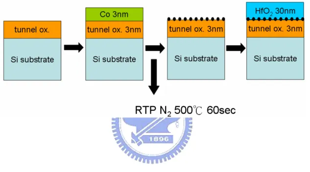
Figure 2-1 presents process flow of an HfO2/Co/SiO2/Si stacked structure. (100)
oriented p-type silicon wafers were chemically cleaned by a standard Radio
Corporation of America cleaning, followed by a 3-nm tunnel oxide was thermally
grown at 1000℃ in vertical furnace system. Subsequently, a 3-nm-thick cobalt layer
was deposited onto the tunnel oxide by electron beam evaporation. The Co
60 s [2.13]. The 30-nm-thick blocking oxide (HfO2) was capped by sputtering. Finally,
Al gate electrode was finally patterned and sintered. The structural analyses were
performed by transmission electron microscopy (TEM). The capacitance-voltage
(C-V) measurements were performed by an HP 4284A precision LCR meter to study
the electron charging and discharging effects of the Co nanocrystals.
2.3 Results and discussions
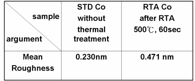
AFM analyses of Co thin film are listed in Table 2-1. Mean roughness of the Co
metal film before and after thermal treatment are 0.230nm and 0.471nm, respectively.
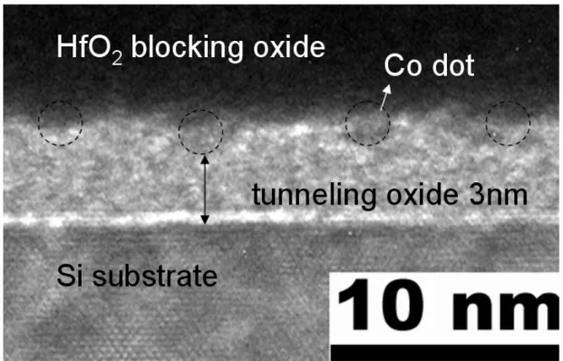
It shows that the Co nanocrystals are formed after thermal treatment. Figure 2-2
presents typical bright-field, cross-section TEM images. It shows the structure of
HfO2/Co/SiO2/Si. As illustrated in Fig. 2-2, the well-separated and spherical Co
nanocrystals embedded between the SiO2 layer and HfO2 layers were observed. The
aerial density and mean size of the Co nanocrystals are measured to be
2.13×10¹²/cm2.and 2 nm, respectively.
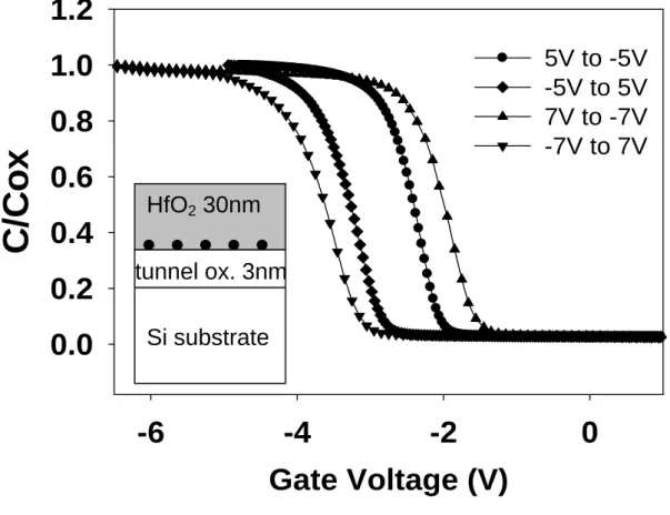
Figure 2-3 shows the forward and reverse sweep C-V characteristics, indicating the
electron charging and discharging effects of Co nanocrystals embedded between the
SiO2 and HfO2 layers. The bidirectional C-V sweeps were performed from deep
inversion to deep accumulation and in reverse, which exhibited electron charging
outstanding threshold voltage shift of 1 V was observed. As the whisked voltage was
increased to 7V, a more obvious C-V shift of 1.8 V was seen. It is perceived that the
hysteresis is counterclockwise which is due to injection of electrons from the deep
inversion layer and injection of holes from the deep accumulation layer of Si substrate.
The result of C-V shift indicates that the charging effects of Co nanocrystals are more
significant than the semiconductor nanocrystals. The high-k blocking oxide
concentrates the electric fields across the tunnel oxide and releases it across the
blocking oxide under program and erase mode. This effect leads to lower program and
erase voltage. Figure 2-4 presents gate voltage dependence of the memory window.
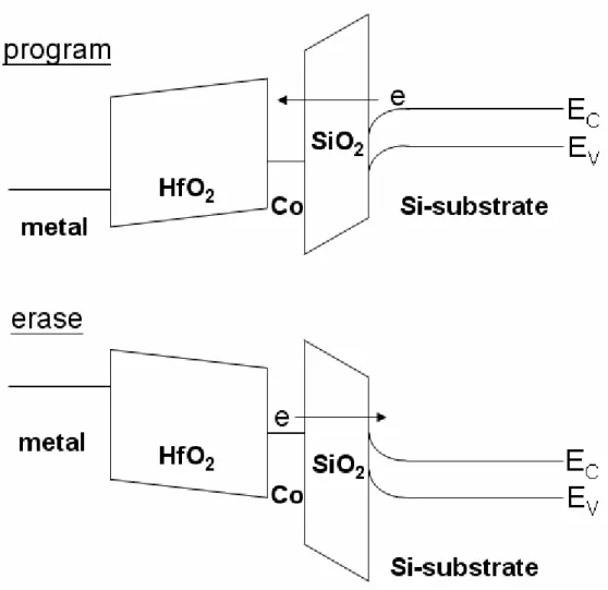
The threshold voltage shift is increased with gate voltage.Figure 2-5 shows the band
diagrams of “program” and “erase” operations with different gate polarities of the
memory device. When the device is written or programmed, the electrons directly
tunnel from the Si substrate through the tunnel oxide, and are trapped in the Co
nanocrystals. On the other hand, as the device is erased, the electrons may tunnel back
to the deep accumulation layer of Si substrate. The blocking oxide is utilized to
prevent the carriers of gate electrode from injecting into the Co nanocrystals by
Fowler-Nordheim tunneling. In addition, the Co nanocrystals do not bear a voltage
drop from gate voltage, which means that all the voltages provided from control gate
semiconductor counterparts. The operating voltage of the memory devices with
conventional floating gate or semiconductor nanocrystals embedded in SiO2 is above
7V. In our approach to fabricate the Co nanocrystals embedded in SiO2, a lower
programming voltage of 5V and erasing voltage of -5 V realize a significant threshold
voltage shift, 1 V, which is sufficient to be defined as “1” and “0” by a typical sensing
amplifier for a memory device.
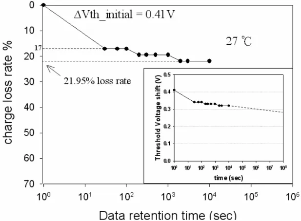
The retention characteristics of the Co nanocrystals were measured at room
temperature, as shown in Fig. 2-6. If there are some leakage paths for the trapping
charges, the memory effect will gradually decrease. In Fig. 2-4, the good retention
characteristics and the memory effect without significant decreasing up to 104 s can be
founded. The charge loss rate only decreases to 21.95% after 104 s. The inset shows
that the threshold-voltage shift does not significantly decrease after long time (104 s).
It is clearly shown that the Co nanocrystals memory has excellent retention
characteristic.
In addition, the reliability of the memory device was also investigated. As shown in
Fig.2-7, the data endurance of the Co nanocrystals memory device retains an obvious
memory window of 0.86 V after 106 cycles and write/erase voltage was 5/(-5) V. The
2.4 Conclusions
In summary, the memory effects of the Co nanocrystals using tunneling and control
oxide, SiO2 and HfO2, were demonstrated in this letter. A significant C-V hysteresis of
Vt shift of 1V is observed under low operating voltage of 5V. The retention
characteristics are tested to be robust. Also, the endurance of the memory device is not
Fig. 2-3 The capacitance-voltage (C-V) hysteresis of Co nanocrystals
memory device after bidirectional sweeps between 5V/(-5V) and
7V/(-7V).
Gate Voltage (V)
-6
-4
-2
0
C/
Cox
0.0
0.2
0.4
0.6
0.8
1.0
1.2
5V to -5V
-5V to 5V
7V to -7V
-7V to 7V
HfO
230nm
Si substrate
tunnel ox. 3nm
Fig. 2-4 Gate voltage dependence of the memory window.
Gate Voltage (V)
0
1
2
3
4
5
6
7
8
9
10
11
12
T
hr
eshol
d vol
tage shi
ft
(
V
)
0
1
2
3
4
5
6
7
Fig. 2-5 The band diagrams of the operation of the distributed charge
storage with Co nano-dots.
Fig. 2-6. Data retention characteristics of the Co nanocrystals memory
device.
Chapter 3
Nickel nanocrystals with HfO
2blocking oxide for nonvolatile
memory application
3.1 Motivation
The commercial products contain poly-Si floating gate (FG) structure which is
taken as charge storage layer. Because of continued scaling of the device structure,
the tunneling oxide must thinner. Once the tunnel oxide is thinner, the electrical
characteristics such as endurance and retention may be degraded. Therefore
memory-cell structures which use discrete traps as the charge storage media have
received much attention. These memories can replace conventional dynamic random
access memory or flash memories for future high speed and low power consuming
memory devices [3.1-3.3]. Nanocrystal memory devices employing distributed
nanodots as storage elements have exhibited great potential in device applications
[3.4-3.10]. Among the different materials of nanocrystals, the metal nanocrystal
memory possesses several advantages: (1) stronger coupling with the conduction
channel; (2) a wide range of available work functions; (3) higher density of states
around the Fermi level; (4) smaller energy perturbation due to carrier confinement
[3.11]. Besides, we use the high-k dielectric as the blocking oxide. Its concentrates
respectively, under the program/erase mode. At the same time, using the high-k
dielectric as the blocking oxide leads to lower program and erase voltage [3.12].In
this study, we demonstrated the memory characteristics of Ni nanocrystals embedded
in SiO2 and HfO2. Because Ni metal has higher work function (~ 4.96eV) than Co
metal(~ 4.41eV). It causes the retention different. Also Ni is compatible with the
current manufacturing technology of semiconductor industry.
3.2 Experimental procedures
Metal-oxide-silicon (MOS) capacitors were fabricated using silicon p-type wafers
[(100) orientation]. Figure 3-1 illustrates the process flow of fabricating Ni
nanocrystals. First, the wafers were chemically cleaned by a standard Radio
Corporation of America cleaning. The thin tunnel oxide (3nm) was thermally grown
at 1000℃ in vertical furnace system. Subsequently, a 3-nm-thick nickel layer was
deposited onto the tunnel oxide by electron beam evaporation. The Ni wetting layer
transformed the Ni nanocrystals after the Rapid thermal annealing (RTA) in the N2
ambient at 500℃ for 60 sec. A 30-nm-thickness blocking oxide (HfO2) was capped
by sputter. The parameter of the high-k sputtering is 0.3 Å/sec as rf power sputter in
150W under the working pressure of 20 mTorr. The flow rate of Ar/O2 is 20/5 SCCM
(SCCM denotes cubic centimeter per minute at STP). The dielectric constant of HfO2
were performed by transmission electron microscopy (TEM). The capacitance-voltage
3.3 Results and discussions
(C-V) measurements were performed by a precision LCR meter HP 4284A to
study the electron charging and discharging effects of the Ni nanocrystals.
Table 3-1 presents AFM analyses of Ni thin film. Mean roughness of the Ni
metal film before and after thermal treatment are 0.229nm and 0.457nm, respectively.
It shows that the Ni nanocrystals are formed after thermal treatment. Figure 3-2 shows
the cross-section TEM of Ni nanocrystal memory structure. The figure presents the
structure of Si substrate/ tunneling oxide/ Ni nanocrystals. The well-separated and
spherical Ni nanocrystals are observed. The higher-resolution image confirms the
presence of Ni nanocrystals of approximately 5 nm in diameter. The aerial density of
the Ni nanocrystals is measured to be 3.9×10¹²/cm2.
Figure 3-3 presents the C-V characteristics of Ni nanocrystals embedded
between the SiO2 and HfO2 layers. It is found that a low operating voltage, 4 V,
causes a significant threshold-voltage shift up to ~ 1 V, which is sufficient to be
defined as ‘‘1’’ or ‘‘0’’ for the logic-circuit design. The electrons of the deep
inversion layer and holes of the deep accumulation layer were injected from the Si
substrate into the nanocrystals, so that the C-V hysteresis is counterclockwise. The
releases it across the blocking oxide under program and erase mode. This effect leads
to lower program and erase voltage. The blocking oxide is utilized to prevent the
carriers of gate electrode from injecting into the Ni nanocrystals by Fowler-Nordheim
tunneling. In addition, the Ni nanocrystals do not bear a voltage drop from gate
voltage, which means all the voltages provided from control gate are dropped to
tunnel oxide and control oxide and gains advantage over their semiconductor
counterparts. Figure 3-4 presents gate voltage dependence of the memory window.
The threshold voltage shift is increased with gate voltage.
The retention characteristics of the Ni nanocrystals were measured at room
temperature, as shown in Fig. 3-5. If there are some leakage paths for the trapping
charges, the memory effect will gradually decrease. In Fig. 3-5, the good retention
characteristics can be founded and the memory effect without significant decreasing
up to 104 s. The charge loss rate only decreases to 15.65% after 104 s. It is clearly
shown that the Ni nanocrystals memory has excellent retention characteristic.
The programming characteristics of Ni nanocrystals memory were studied by
stressing samples with a pulse voltage of ±5 V and a pulse width of 5 ms during
programming and erasing (P/E). Figure 3-6 shows the endurance characteristics of Ni
nanocrystals memory after different stressing cycles at room temperature. The
There was no degradation of the threshold voltage shift observed even after 106 P/E
cycles.
3.4 Conclusions
In summary, the nonvolatile memory device with Ni nanocrystals exhibits 1 V
threshold voltage shift under 4 V write operation, which is sufficient for a memory
device to define the signal “0” and “1”. The device has a long retention time with a
small charge lose rate. Besides, the endurance of the memory device is not degraded
up to 106 write/erase cycles.
3.5 Retention characteristics different with Co and Ni nanocrystals
memory device
This section discusses the retention different between Co and Ni nanocrystals
memory device. Fig. 3-7 shows the retention characteristic for Co and Ni nanocrystals
memory device. The charge loss rate of Co metal and Ni metal are 21.95% and
15.65% respectively after 104 s. The charge loss rate of Co metal is more than Ni
metal. Because Ni metal has higher work function (~ 4.96eV) than Co metal(~ 4.41eV)
as shown in Fig. 3-8. Fig. 3-8 presents band diagram of Ni and Co nanocrystals
nonvolatile memory during retention. The electrons tunnel from the Si substrate
metal nanocrystals. The band offset between SiO2 tunnel oxide and nanocrystals
become high due to high work function of metal. The higher band offset between
SiO2 tunnel oxide and nanocrystals, the more difficult electrons go back Si substrate
from nanocrystals. The work function of Ni metal is about 4.96eV. Its more than Co
metal(~ 4.41eV). Therefore the retention characteristic of Ni nanocrystals is better
Fig. 3-2. Cross-section TEM micrographs of an Ni/SiO
2/Si stacked
structure.
Fig. 3-3. The capacitance-voltage (C-V) hysteresis of Ni nanocrystals
memory device after bidirectional sweeps between 4V/(-4V) and
5V/(-5V).
Fig. 3-4 Gate voltage dependence of the memory window.
Gate Voltage (V)
0
1
2
3
4
5
6
7
T
hr
e
s
h
ol
d vol
tage shi
ft
(
V
)
0.0
0.5
1.0
1.5
2.0
2.5
Fig. 3-5. The retention characteristics of the Ni nanocrystals memory
device at room temperature.
Fig. 3-6. The endurance characteristics of the Ni nanocrystals memory
device at room temperature.
Chapter 4
Fabrication and electrical characteristics of CoSi nanocrystals
nonvolatile memory with HfO
2blocking oxide for memory device
applications
4.1 Motivation
The lots produced nonvolatile memory devices are based on the concept of a
continuous layer of floating gate up to now [4.1]. Although many popular products are
made by nonvolatile memory devices, it still has the difficulties of continue scaling
down [4.2]. It must compromise between long-term nonvolatility and high operating
speed [4.3]. Therefore the concept of distributed storage of charge has caught a lot of
attention lately. Tiwari et al. [4.4] was the first time demonstrated the Si nanocrystal
floating gate memory device in the early nineties to solve the scaling limits of the
conventional FG structure. The nanocrystal memory device can not only maintain
good retention characteristics when tunnel oxide is thinner but also lower the power
consumption [4.4-4.13]. Direct forming of the metal nanocrystals from metal (Co,Ni)
films have many problems. For example, the size of metal nanocrystals cannot be
controlled. The metal nanocrystals have more active with other materials during the
processes. It may cause the devices failure. So we search the materials which are more
desirable for applications of the nonvolatile memory technology.
4.2 Experimental procedures
Silicon p-type wafers [(100) orientation] were chemically cleaned by a standard
Radio Corporation of America cleaning. The 3-nm tunnel oxide was thermally grown
at 1000℃ in vertical furnace system.Subsequently, 3-nm a-Si layer and 3-nm Cobalt
layer were deposited onto the tunnel oxide by electron beam evaporation.As shown in
figure 4-1, the stacked structure was oxidized at 700℃ for 5 minutes to form CoSi
nanocrystals. The nanocrystals were identified to be CoSi phase by the analysis of
electron diffraction pattern shown in figure 4-2 [4.14]. A 30-nm-thickness blocking
oxide (HfO2) was capped by sputter. Finally, Al gate electrode was finally patterned
and sintered. The structural analyses were performed by transmission electron
microscopy (TEM). The capacitance-voltage (C-V) measurements were performed by
a precision LCR meter HP 4284A to study the electron charging and discharging
effects of the CoSi nanocrystals.
4.3 Results and discussions
Figure 4-3 shows the capacitor-gate voltage(C-V) characteristics of CoSi
nanocrystal embedded between the SiO2 and HfO2 layers. The electrical C-V
measurements are performed by bidirectional voltage sweep. In Fig. 4-3, with the
1.6 V is observed. As the swept voltage is increased to 12V, a more pronounced C-V
shift is observed. The electrons of the deep inversion layer and holes of the deep
accumulation layer were injected from the Si substrate into the nanocrystals, so that
the C-V hysteresis is counterclockwise. The high-k blocking oxide concentrates the
electric fields across the tunnel oxide and releases it across the blocking oxide under
program and erase mode. This effect leads to lower program and erase voltage. The
blocking oxide is utilized to prevent the carriers of gate electrode from injecting into
the CoSi nanocrystals by Fowler-Nordheim tunneling. In addition, the CoSi
nanocrystals do not bear a voltage drop from gate voltage, which means all the
voltages provided from control gate are dropped to tunnel oxide and control oxide and
gains advantage over their semiconductor counterparts. The inset was the
cross-section TEM of CoSi nanocrystals memory structure. It presents the structure of
Si substrate/ tunneling oxide/ CoSi nanocrystals/ HfO2 blocking oxide. The
well-separated and spherical Ni nanocrystals are observed.
In Fig.4-4, the charge retention characteristics of the CoSi nanocrystals were
measured at room temperature. If there are some leakage paths for the trapping
charges, the memory effect will gradually decrease. In Fig.4-4, the good retention
characteristics can be founded and the memory effect without significant decreasing
threshold voltage shift versus time. It is clearly shown that the CoSi nanocrystals
memory has excellent retention characteristic.
The reliability of memory is major issue for nonvolatile memory devices. The
endurance of CoSi nanocrystals memory were studied by stressing samples with a
pulse voltage of ±7 V and a pulse width of 5 ms. Figure 4-5 shows the endurance
characteristics of CoSi nanocrystals memory after different stressing cycles. The
threshold voltage shift versus stressing cycles shows superior endurance. There was
no significant degradation (only 17.1%) of the threshold voltage shift observed even
after 106 P/E cycles.
4.4 Conclusions
In conclusion, the nonvolatile memory device with CoSi nanocrystals exhibits
1.6 V threshold voltage shift under 9 V write operation, which is sufficient for a
memory device to define the signal “0” and “1”. The device has a long retention time
with a small charge lose rate. Besides, the endurance of the memory device is not
Fig. 4-2. The electron diffraction pattern corresponding to CoSi
nanocrystals.
Fig. 4-3. The capacitance-voltage (C-V) hysteresis of CoSi nanocrystals
memory device after bidirectional sweeps between 9V/(-9V) and
12V/(-12V). The inset is cross-section TEM micrographs of an
HfO
2/CoSi/SiO
2/Si stacked structure.
Gate Voltage (V)
-8
-6
-4
-2
0
C/
C
ox
0.0
0.2
0.4
0.6
0.8
1.0
1.2
9V to -9V -9V to 9V 12V to -12V -12V to 12VFig. 4-4. Data retention characteristics of the CoSi nanocrystals memory
device.
Fig. 4-5. Endurance characteristics of the CoSi nanocrystals memory
device.
Chapter 5
Nickel silicide nanocrystals embedded in SiO
2and HfO
2for
Nonvolatile Memory Application
5.1 Motivation
Nonvolatile memory is a necessary indispensable component of modern
electronic systems. Nonvolatile memory is used in personal computers, cellular
phones, digital cameras, global positioning systems, etc. Conventional floating-gate
(FG) devices have their limitations, because of continued scaling of the device
structure. The tunnel oxide is thinner with the continued scaling down. So the
retention characteristics of memory devices may be degraded [5.1]. Recently,
memory-cell structure using discrete traps as the charge storage media has received
much attention as the promising candidate to replace conventional dynamic random
access memory or flash memories for future high speed and low power consuming
memory devices [5.2-5.3]. Nanocrystals memory devices employing distributed
nanodots as storage elements have exhibited great potential in device applications
[5.4-5.10]. Among the different materials of nanocrystals, the metal nanocrystals
memory possesses several advantages, such as stronger coupling with the conduction
channel, a wide range of available work functions, higher density of states around the
using the high-k dielectric as the blocking oxide concentrates and releases the electric
fields across the tunnel oxide and the blocking oxide, respectively, under the
program/erase mode. Using a high-k dielectric as the blocking oxide leads to lower
program and erase voltage [5.11].
5.2 Experimental procedures
(100) oriented p-type silicon wafers were chemically cleaned by a standard
Radio Corporation of America cleaning, followed by formation of a 3-nm tunnel
oxide layer which was thermally grown at 1000℃ in a vertical furnace system.
Subsequently, a 3-nm amorphous silicon layer and a 3-nm-thick nickel layer were
deposited onto the tunnel oxide by electron beam evaporation, respectively. In
addition, a 10-nm amorphous silicon layer was deposited on some of the samples.
Oxidation at 800℃ 700℃ and 600 ℃ was performed at 5min, 10min and 10min
respectively to form nickel silicide nanocrystals. The 30-nm-thickness blocking oxide
(HfO2) layer was deposited by sputtering. Finally, an Al gate electrode was
patterned and sintered. Figure 5-1 presents the process flow. The structural analyses
were performed by transmission electron microscopy (TEM). The capacitance-voltage
(C-V) measurements were performed by a precision LCR meter HP 4284A to study
the electron charging and discharging effects of the nickel silicide nanocrystals.
Figure 5-2 shows the forward and reverse sweep C-V characteristics, indicating
the electron charging and discharging effects of nickel silicide nanocrystals embedded
between the SiO2 and HfO2 layers. The bidirectional C-V sweeps were performed
from deep inversion to deep accumulation and in reverse, which exhibited an electron
charging effect. In Fig. 5-2, with the voltage swept from 8 to -8V and back to 8 V, an
outstanding threshold voltage shift of 0.7 V was observed. As the whisked voltage
was increased to 10V, a more obvious C-V shift of 1.3 V was seen. It is perceived that
the hysteresis is counterclockwise which is due to injection of electrons from the deep
inversion layer and injection of holes from the deep accumulation layer of Si substrate.
The resulting C-V shift indicates that the charging effects of nickel silicide
nanocrystals are more significant than that seen for semiconductor nanocrystals. The
high-k blocking oxide concentrates the electric fields across the tunnel oxide and
releases it across the blocking oxide under program and erase mode. This effect leads
to lower program and erase voltage. When the device is written or programmed, the
electrons directly tunnel from the Si substrate through the tunnel oxide, and are
trapped in the nickel silicide nanocrystals. On the other hand, as the device is erased,
the electrons may tunnel back to the deep accumulation layer of the Si substrate. The
blocking oxide is utilized to prevent the carriers from the gate electrode from being
In addition,the nickel silicide nanocrystals do not exhibit a voltage drop fromthe gate
voltage, which means all the voltages provided from control gate are dropped to
tunnel oxide and control oxide and this provides an advantage over their
semiconductor counterparts. Figure 5-3 presents the cross-section TEM micrographs
of an HfO2/nickel silicide /SiO2/Si stacked structure with dry oxidation at 600℃. As
illustrated in Fig. 5-3, well-separated and spherical nickel silicide nanocrystals were
observed between the SiO2 layer and HfO2 layers. The nanocrystals were identified to
be a NiSi2 phase through analysis of the diffraction ring pattern shown in Fig. 5-4.
Figure 5-5 shows the capacitance-voltage (C-V) hysteresis of sample with
α-Si/Ni/α-Si structure after dry oxidation at 700℃. It was found that as the voltage
swept from 8 to -8V and back to 8 V, significant threshold voltage shift of 1.7 V was
observed. When the whisked voltage was increased to 10V, a more obvious C-V shift
of 2.1 V was seen. For samples oxidized at 600℃, these voltages were larger shift. In
figure 5-6, the voltage swept from 3 to -3V and back to 3 V, a threshold voltage shift
of 0.4 V was observed. When the whisked voltage was increased to 5V, a more
obvious C-V shift of 2 V was seen. Figure 5-7 presents the threshold voltage vs.
operation voltage for samples oxidized at different temperature. The sample which
used α–Si/Ni/α-Si structure had improved memory characteristics. As shown in
distribution between SiO2 and HfO2. It was different from the α–Si/Ni conventional
device(distribution of plane) [5.10][5.12]. It shows that more charges were injected
into deep nickel silicide nanocrystals under programming mode. The charges which
were injected into deep nickel silicide nanocrystals resulted in the higher threshold
voltage. The operating voltage of the memory devices with a conventional floating
gate or semiconductor nanocrystals embeddedin SiO2 is above 7V [5.13-5.14]. In our
approach to fabricate the nickel silicide nanocrystals embedded in SiO2 and HfO2, a
lower programming voltage of 4V and erasing voltage of -4 V realizes a significant
threshold voltage shift, 1.3 V, which is sufficient to be defined as “1” and “0” by a
typical sensing amplifier for a memory device.
5.4 Conclusions
A nonvolatile memory device with NiSi2 nanocrystals embedded in the SiO2 and
HfO2 layer has been fabricated. A significant memory effect is observed through the
electrical measurements. When a low operating voltage, 4V, is applied a significant
threshold-voltage shift, 1.3V, is observed. The processing of the structure is
Fig. 5-2 The capacitance-voltage (C-V) hysteresis of nickel silicide
nanocrystals memory device after bidirectional sweeps between 8V/(-8V)
and 10V/(-10V).
Gate Voltage (V)
-6
-4
-2
0
2
C/Cox
0.0
0.2
0.4
0.6
0.8
1.0
1.2
8V to -8V
-8V to 8V
10V to -10V
-10V to 10V
Fig. 5-3 The cross-section TEM micrographs of an HfO
2/nickel silicide
/SiO
2/Si stacked structure.
Fig. 5-4 The electron diffraction pattern corresponding to nickel silicide
nanocrystals.
Fig. 5-5 The capacitance-voltage (C-V) hysteresis of sample with
α-Si/Ni/α-Si structure after dry oxidation at 700℃.
Gate Voltage (V)
-4
-2
0
2
4
C/
Co
x
0.0
0.2
0.4
0.6
0.8
1.0
1.2
5V to -5V
-5V to 5V
8V to -8V
-8V to 8V
10V to -10V
-10V to 10V
Dry Oxidation 700C 10min
Figure 3b
Fig. 5-6 The capacitance-voltage (C-V) hysteresis of sample with
α-Si/Ni/α-Si structure after dry oxidation at 600℃.
Dry Oxidation 800C 5min
Gate Voltage (V)
-4
-2
0
2
4
C/
Cox
0.0
0.2
0.4
0.6
0.8
1.0
3V to -3V
-3V to 3V
4V to -4V
-4V to 4V
5V to -5V
-5V to 5V
Dry Oxidation 600C 10min
Fig. 5-7 The memory window vs. (program/erase) voltage of nickel
silicide nanocrystal memory.
Chapter 6
Using double layer CoSi
2nanocrystals to improve the memory effects
of nonvolatile memory devices
6.1 Motivation
Memory devices employing distributed nanocrystals as storage elements have
exhibited great potential to replace conventional dynamic random array memory or
flash memories for future high speed and low power consumer memory devices
[6.1-6.5]. Nanocrystalline silicon was introduced as a replacement for the
conventional floating gate in the nonvolatile memory structure by Tiwari et al[6.1].
To date, most studies have focused on the fabrication on Si and Ge nanocrystals in
metal-oxide-semiconductor structure [6.6-6.11]. The use of a floating gate composed
of distributed nanocrystals reduces the problems of charge loss encountered in
conventional floating-gate electrically erasable programmable read-only memory
devices. It allows thinner tunnel oxide and, thereby, smaller operating voltages, better
endurance and retention, and faster program/erase speed [6.12-6.13].
The metal nanocrystals memory possesses several advantages, such as
stronger coupling with the conduction channel, a wide range of available work
functions, higher density of states around the Fermi level and smaller energy