國立交通大學
電子工程學系 電子研究所碩士班
碩 士 論 文
低溫複晶矽玻璃基板上之
液晶顯示器驅動電路設計
On-Glass Driving Circuits Design for LCD
in LTPS Technology
研 究 生 : 黃如琳
指導教授 : 柯明道 教授
摘要 i
低溫複晶矽玻璃基板上之
液晶顯示器驅動電路設計
研究生: 黃如琳
指導教授: 柯明道 教授
國立交通大學
電子工程學系 電子研究所碩士班
摘要
本論文利用低溫複晶矽的製程,將液晶顯示器驅動電路設計並實現在玻璃基 板上。液晶顯示器的驅動電路主要分為閘級驅動電路及源級驅動電路;其中閘級 驅動電路包含移位暫存器、電位轉換器和輸出緩衝器;而源級驅動電路則是由移 位暫存器、閂鎖器、電位轉換器、數位對類比轉換器及輸出電壓緩衝器組成。 本論著重於將源級驅動電路實現在玻璃基板上。由於液晶顯示器具有高負載 的特性,所以在輸出電壓緩衝器的部分,本論文設計了兩種具有驅動高負載功能 的電路,分別為具有高旋轉率和低功率消耗的 B 類電壓輸出緩衝器。此外,也 針對了低溫複晶矽的臨界電壓漂移問題,設計了一個具有臨界電壓補償的輸出緩 衝器;在數位對類比轉換器的方面,因為液晶之穿透率和偏壓電位成一非線性關 係,所以本論文也設計了一個具有珈瑪修正功能的數位對類比轉換器來補償這效 應;在電位轉換器的部分,本論文則是以基底加偏壓的方式,並利用台積電 0.35-µm CMOS 的高壓製程,模擬且分析在不同偏壓下其操作速度和功率消耗的 關係。而以上的電路皆以統寶的 6-µm 或 3-µm 低溫複晶矽製程實現。 最後,為了滿足高解析度的液晶顯示器,源級驅動電路在資料的接收端上, 常會使用 RSDS 的規格來做傳輸介面,以增加其資料的傳輸速度並克服電磁干擾 的效應,所以本論文也嘗試利用統寶的 6-µm 低溫複晶矽製程,設計一 RSDS 接 收端的基本驅動電路。Abstract ii
On-Glass Driving Circuits Design for LCD
in LTPS Technology
Post-graduate: Ju-Lin Huang Advisor: Prof. Ming-Dou Ker
Department of Electronics Engineering & Institute of Electronics
National Chiao-Tung University
ABSTRACT
In this thesis, on-glass driving circuits for LCD are designed and implemented in low temperature poly silicon (LTPS) technology. The driving circuits for LCD are divided into two parts, gate driver and source driver. Gate driver includes shift registers, level shifters, and output buffers. Source driver is composed of shift registers, latches, level shifters, a digital to analog converter, and output buffers.
The implement of the on-glass source driver is the focus in this thesis. First, two circuits, which are slew rate enhancement output buffer and low power class-B output buffer, are designed to drive the heavy loading of LCD. Second, a threshold voltage compensation circuit is proposed to solve the drift of the threshold voltage in LTPS process. Third, due to the nonlinear relationship between transparency and voltage across liquid crystal, a digital to analog converter with gamma correction is adopted to compensate this effect. Finally, level shifters using body-bias technique are also proposed. According to TSMC 0.35-µm CMOS HV process, the operational speed and power consumption of level shifters in different body-bias voltages are simulated and analyzed. All of above circuits have been implemented in TOPPOLY 6-µm or 3-µm LTPS process.
Moreover, in order to satisfy the high resolution LCD, source driver usually employs the specification for reduced swing differential signaling (RSDS) as the transition interface in the data receiver. Besides, the application of the specification for RSDS will increase the data transition speed and reduce the electric magnetic interference (EMI) effect. So, a fundamental RSDS receiver in TOPPOLY 6-µm LTPS process is also included in this thesis.
誌謝 iii
誌謝
首先,感謝我的指導老師柯明道教授,在碩士這兩年的求學過程中,不厭其 煩的指導我,讓我不僅學到如何有效率的做研究,更學會如何嚴謹的看待問題。 再來,要感謝統寶光電的蔡耀銘副處長、林敬偉課長和所有幫助過我的學長 們,由於你們全力的支援與幫忙,我的電路才得以順利的下線,也才能有今日的 研究成果。同時,也要感謝實驗室學長和同學們精神上的支持,甚或實質上的協 助,我才能有幸完成本論文。例如徐振洲學長、鄧至剛學長、陳世倫學長、陳榮 昇學長和黃鈞正學長等,當然還有一起打拼的實驗室同學,包括聖文、阿爛、瑋 仁、秉捷、志松、史周、阿瑞、權哲、棋樺、宗霖、韋霆、致遠、旻珓、丁彥、 紀豪等。此外,可能尚有一些未提及的朋友們,在此均一併致謝。 最後,我要感謝我的父母與家人,若不是他們一直在背後默默的支持,也不 會有我今天這小小的成果。特別是我的父母,由於你們開明的態度,才讓我有自 由發展興趣的機會,真的非常感激你們。當然,也要謝謝我的女友陳育萱,感謝 她總是能在我感到挫折時,聆聽我的心情並給予我許多建議和鼓勵。我在撰過程 中,雖力求嚴謹,然誤謬之處,在所難免,尚祈各位讀者賜予寶貴意見,使本論 文能更加完善。 黃如琳 國立交通大學 中華民國九十三年六月Contents iv
CONTENTS
CHINESE
ABSTRACT
i
ENGLISH
ABSTRACT
ii
ACKNOWLEDGEMENTS
iii
CONTENTS
iv
TABLE
CAPTIONS
vii
FIGURE
CAPTIONS viii
CHAPTER1
INTRODUCTION
1
1.1 Motivation 1
1.2 Thesis Organization 2
CHAPTER2 BACKGROUND OF LIQUID CRYSTAL
DISPLAY
4
2.1 Liquid Crystal Display Structure 4 2.1.1 Liquid Crystal 4 2.1.2 Structure of LCD 5 2.2 Driving Method in LCD 5
2.2.1 Gamma Correction 6 2.2.2 Driving Method 6 2.3 Periphery Circuit Block 7
2.3.1 Scan Driver Circuit 8 2.3.2 Data Driver Circuit 8
Contents v
CHAPTER3 OUTPUT BUFFER WITH THRESHOLD
VOLTAGE
COMPENSATION 17
3.1 Design Consideration of Output Buffer for LCD 17 3.1.1 Rail-to-Rail Operational Amplifier 18 3.1.2 High Slew Rate Operational Amplifier 18 3.2 Slew Rate Enhancement Output Buffer 19 3.3 Low Power Class-B Output Buffer 21
3.3.1 Design Conception 21 3.3.2 Measurement Result 24 3.4 Output Buffer with VTHCompensation 25 3.4.1 The Causation of Offset Voltage 25 3.4.2 Design of Output Buffer with VTH Compensation 28
CHAPTER4 GAMMA CORRECTION DAC FOR LCD
51
4.1 Digital to Analog Converter 51 4.1.1 Resistor-String DAC 51 4.1.2 Charge-Redistribution DAC 52 4.1.3 Hybrid DAC Architecture 52 4.2 Gamma Correction DAC 53
4.2.1 Design of Gamma Correction DAC 53 4.2.2 Measurement Result 55 4.2.3 Analysis in Resistor and Capacitor Sample 55
CHAPTER5 LEVEL SHIFTER USING BODY BIAS
70
5.1 SOI CMOS with Body Bias 70 5.2 Level Shifter with Body Bias 71 5.2.1 TFT Device with Body Bias 71 5.2.2 Level Shifter Using Body Bias Technique 72
CHAPTER6 DESIGN DRIVER CIRCUIT FOR RSDS
RECEIVER
84
Contents vi
6.2 Driver Circuit for RSDS Receiver 85 6.2.1 Design Concept of RSDS Receiver 85 6.2.2 Architecture of RSDS Receiver 86
CHAPTER7 CONCLUSIONS AND FUTURE WORKS
92
7.1 Conclusions 92
7.2 Future Works 93
REFERENCES
94
Table Captions vii
TABLE CAPTIONS
Table I Operation frequencies specification of LCD panel. 31
Table II Specification of slew rate enhancement output buffer. 31
Table III Specification of Class-B output buffer. 32
Table IV The relationship between phase margin and overshot. 32
Table V The resistor values of resistor string. 57
Table VI The measurement results of gamma correction DAC. 57
Table VII The resistor values of resistor string. 58
Table VIII The simulation results of LS_C, LS_G and LS_D. 76
Table IX The specification of RSDS which is proposed by NS Corp. 87
Table X The specification of LVDS which is proposed by NS Corp. 87
Figure Captions viii
FIGURE CAPTIONS
Fig. 2.1 Phase variation of liquid crystal in different temperature.
Fig. 2.2 Transparency of TN and STN in different voltage.
Fig. 2.3 Cross section of LCD module.
Fig. 2.4 The liquid crystal operates in normally white case: (a) light can pass and
(b) light is blocked.
Fig. 2.5 (a) The relationship between digital input codes and input voltage across
liquid crystals and (b) the smooth curve between digital input codes and light transmission rate.
Fig. 2.6 Inversion of LCD panel.
Fig. 2.7 The operational waveform of direct driving method.
Fig. 2.8 The operational waveform of AC modulation driving method.
Fig. 2.9 Block diagram of the LCD panel driver circuits.
Fig. 2.10 The pixel layout structure of active matrix cell on LCD panel.
Fig. 2.11 The block diagram of scanning driver.
Fig. 2.12 RC (resister and capacitor) ladder of scanning line. Fig. 2.13 The block diagram of data driver.
Fig. 3.1 The values of RC ladder in Samsung data sheet.
Fig. 3.2 An elegant and lower power rail-to-rail amplifier.
Fig. 3.3 A fundamental circuit structure of slew rate enhancement.
Fig. 3.4 A simple operational amplifier with slew rate enhancement.
Fig. 3.5 AC simulation of slew rate enhancement output buffer.
Fig. 3.6 Output waveform of slew rate enhancement output buffer.
Fig. 3.7 Layout of slew rate enhancement output buffer.
Fig. 3.8 A low power class-B output buffer.
Fig. 3.9 AC simulation of class-B output buffer.
Fig. 3.10 Output waveform of class-B output buffer.
Fig. 3.11 Layout of class-B output buffer.
Fig. 3.12 The input pattern and DC bias are generated by pulse generation and power supply through probe station.
Fig. 3.13 Instruments for measuring class-B output buffer.
Fig. 3.14 The output waveform when input signal swing is 2V-10V and opera- tional frequency is 50 kHz.
Fig. 3.15 The output waveform when input signal swing is 5.75V-6.25V and operational frequency is 50 kHz.
Figure Captions ix
Fig. 3.16 The output waveform when input signal swing is 2V-10V and opera- tional frequency is (a) 100 kHz, (b) 200 kHz, (c) 400 kHz and (d) 800 kHz.
Fig. 3.17 The output waveform when input signal swing is 5.75V-6.25V and operational frequency is (a) 100 kHz, (b) 200 kHz, (c) 400 kHz and (d) 800 kHz.
Fig. 3.18 The structure of data driver in TFT-LCD.
Fig. 3.19 The gate dimensions of the TFT device suffer from random and micro- scopic variations.
Fig. 3.20 (a) The conventional operational amplifier with offset voltage measured at the output, (b) circuit of (a) with its offset voltage referred to the input.
Fig. 3.21 The input referred offset voltage of the N-type TFT and P-type TFT. Fig. 3.22 Circuit diagram of analog output buffer with three-phase threshold
voltage compensation.
Fig. 3.23 Waveform diagram of analog output buffer with three-phase threshold voltage compensation.
Fig. 3.24 Layout of output buffer with three-phase threshold voltage compen- sation.
Fig. 3.25 Circuit diagram of analog output buffer with two-phase threshold voltage compensation.
Fig. 3.26 Waveform diagram of analog output buffer with two-phase threshold voltage compensation.
Fig. 3.27 Layout of output buffer with two-phase threshold voltage compensation.
Fig. 3.28 The relationship between VTH and output variation when Vin = 10 V.
Fig. 3.29 The relationship between VTH and output variation when Vin = 2 V.
Fig. 3.30 A secondary analog output buffer with modified two-phase threshold voltage compensation.
Fig. 3.31 Waveform diagram of secondary analog output buffer with modified two-phase threshold voltage compensation.
Fig. 3.32 Layout of secondary analog output buffer with modified two-phase threshold voltage compensation.
Fig. 3.33 The relationship between VTH and output variation when Vin = 8 V.
Fig. 3.34 The relationship between VTH and output variation when Vin = 2 V.
Fig. 4.1 DAC using tree-like decoder.
Fig. 4.2 DAC using digital decoder.
Figure Captions x
Fig. 4.4 A hybrid structure of gamma correction DAC.
Fig. 4.5 (a) shows the transparency versus operation voltage of liquid crystal and
(b) shows the input codes versus transparency.
Fig. 4.6 Input codes versus operational voltage.
Fig. 4.7 A 6-to-64 gray level gamma correction DAC with resistor-string archi-
tecture.
Fig. 4.8 The simulation waveform of gamma correction DAC with resistor-string
architecture.
Fig. 4.9 The definitions of (a) offset error and (b) gain error.
Fig. 4.10 The definition of INL error.
Fig. 4.11 Delta of the proposed gamma correction DAC.
Fig. 4.12 INL error of the proposed gamma correction DAC.
Fig. 4.13 The full layout in TOPPOLY 6-µm LTPS process.
Fig. 4.14 The glass sample of gamma correction DAC.
Fig. 4.15 The measurement result of (a) N-TFT device and (b) P-TFT device. Fig. 4.16 The simulation result of (a) N-TFT device and (b) P-TFT device. Fig. 4.17 The boding diagram of 6-to-64 gray level gamma correction DAC Fig. 4.18 The measurement result of delta.
Fig. 4.19 The measurement result of INL error.
Fig. 4.20 The resistor samples made in metal1 which ratio are 6:3:2 in layout. Fig. 4.21 The deviations of resistors in different glass panels.
Fig. 4.22 The deviations of capacitors in different glass panels.
Fig. 5.1 (a) is the cross section of SOI NMOS device and (b) is the T-gate
DTMOS (dynamic threshold MOS).
Fig. 5.2 Layout technique of body contact.
Fig. 5.3 The whole layout of N-TFT device with body bias.
Fig. 5.4 The IV curve with different body bias.
Fig. 5.5 The relationship between threshold voltage and body bias.
Fig. 5.6 The structure of driver circuit for LCD panel.
Fig. 5.7 (a) is conventional level shifter (LS_C); (b) and (c) are two modified
level shifter LC_D and LS_G, respectively.
Fig. 5.8 The comparisons of rise time.
Fig. 5.9 The comparisons of fall time.
Fig. 5.10 The comparisons of delay time.
Fig. 5.11 The comparisons of power consumption.
Figure Captions xi
Fig. 6.1 System diagram of the LCD panel.
Fig. 6.2 The first type driver circuit for RSDS receiver.
Fig. 6.3 The second type driver circuit for RSDS receiver.
Fig. 6.4 Simulation result of the first type driver circuit for RSDS receiver.
Fig. 6.5 Layout diagram of the first type driver circuit for RSDS receiver.
Fig. 6.6 Simulation result of the second type driver circuit for RSDS receiver.
Chapter 1 1
CHAPTER 1
INTRODUCTION
1.1 Motivation
With information technology (IT) industry progressing, LCD (liquid crystal display) becomes the central feature of many consumer products. The main consideration of LCD performance is high resolution, wide view-angle, and high contrast ratio, etc. Besides, a current trend of LCD is lower power, light weight, and small volume. Based on the above descriptions, some fundamental requirements for LCD are listed below as a reference:
z Full color (8 bits/color).
z High resolution (200 dots per inch). z Large panel size (960 × 1100 mm2
). z Wide view angle (180° both axes). z High contrast ratio (200:1).
z Light weight (2.5g/cm2 ). z Small volume (0.5 mm). z Low power.
Furthermore, LTPS (low temperature poly silicon) technology is the novel technology specific for LCD application. The manufacture of LTPS is apparently more complicated than amorphous poly silicon technology, but LTPS TFT (thin film transistor) has 100 times high mobility than amorphous silicon (α-Si) TFT and can carry out CMOS process on the glass substrate. Some advantages for LTPS over
Chapter 1 2
amorphous poly silicon are shown below:
z Slimmer peripheral dimension: Capability for integrating driving circuit on glass substrate is better, which means slimmer peripheral dimension and low cost.
z High aperture: The LTPS TFT device with high mobility can achieve a short charging time by small size and so that it contributes more pixel area to light transition.
z Compatible for OLED (organic light emitting diode): The LTPS TFT device with high mobility can provide high-current driving capability for OLED application.
z Compact module: Less PCB (printed circuit board) area is required due to driver integrated on glass.
According to above discussion, it can see that the fabrication cost will gradually be lowed and SOP (system on panel) will be implemented step by step in the future. Moreover, LTPS technology is compatible with OLED, which is another promising display device. Therefore, design of driving circuit for LCD in LTPS technology is worthy expecting in the future.
1.2 Thesis Organization
In this thesis, an on-glass data driver is designed and implemented to satisfy the specification for LCD in TOPPOLY 6-µm LTPS process. Furthermore, a fundamental RSDS receiver in TOPPOLY 6-µm LTPS process has also been included and discussed in this thesis. And the main point of each chapter is described in below.
Chapter 1 3
In chapter 3, a slew rate enhancement and a low power class-B output buffer are designed. Besides, in order to overcome the variation of VTH (threshold voltage) in output buffer, an output buffer with VTH compensation is also proposed.
In chapter 4, a 6-to-64 gray level DAC with gamma correction are proposed and implemented to solve the nonlinear-transparency characteristics in liquid crystals.
In chapter 5, the function of a TFT device with body bias is verified. Furthermore, some modified level shifters by body bias technique are also proposed and analyzed in this chapter.
In chapter 6, a fundamental RSDS receiver is also included to increase the data transition speed and to reduce the electric magnetic interference (EMI) effect in data transition.
Chapter 2 4 4
CHAPTER 2
BACKGROUND OF LIQUID CRYSTAL DISPLAY
2.1 Liquid Crystal Display Structure
2.1.1 Liquid Crystal
Liquid crystal is a phase of matter whose order is intermediate between that of a liquid and that of a crystal. The phase variation of liquid crystal in different temperature is shown in Fig. 2.1. And the molecules are typically rod-shaped organic moieties about 25 Angstroms in length and their ordering is a function of temperature [1]-[3]. In addition, the molecular orientation can be controlled with applying various electric fields.
According to the way that liquid crystals are formed, it can be distinguished into thermotropic and lyotropic liquid crystals. For lyotropic liquid crystals, the phases formed depend upon the nature of the molecules involved, the temperature, and the type of solvent. In themotropic liquid crystals, the phase formed is characteristic of the temperature. But, if base on the arrangement of liquid crystal molecules, liquid crystals can be divided into three types — smetcic, nematic and cholesteric.
Because the twist of liquid crystals can be controlled by the electric field that is applied across it, liquid crystals are used as a switch that passes or blocks the light. TN (twisted nematic) and STN (super twisted nematic) are the terms used to describe two types of liquid crystal displays. TN displays have a twist of 90 degrees or less. And almost all active matrixes have a 90 degree twist. As the name implies, STN displays have a twist that is greater than 90 but less than 360 degrees. Currently most
Chapter 2 5 5 STN displays are made with a twist between 180 and 240 degrees. The higher twist angle causes steeper threshold curve which puts the on and off voltages closer together. As a result, it is usually applied in passive matrixes. And the transparency of TN and STN in different voltage is illustrated in Fig. 2.2.
2.1.2 Structure of LCD
The cross section of LCD with polarizer, glass, LC (liquid crystal) material, and color filter is shown in Fig. 2.3. Polarizer can be divided into top polarizer and bottom polarizer. The top polarizer can polarize the incident light from random polarization into unique one. Before electric field is applied on the electrodes, the liquid crystals are aligned in a twist pattern. The path of light is then changed with the twist pattern of the liquid crystals. The bottom polarizer is aligned opposite of the top polarizer. Consequently, when the light reaches the bottom polarizer, they will align with each other and the light can pass through, which is illustrated in Fig. 2.4(a). On the contrary, if the electric is applied on the electrode, the liquid crystals will turn to the same direction. Then, the light can not pass the bottom polarizer, which is shown in Fig 2.4(b). In this case, it is usually called normally white.
The multiple step-and-repeat images of the LCD electrode on glass substrate are created by precise photolithography technique. TFT glass has so many TFT as the number of pixels while color filter glass has color filter that generates color. Three primary colors, red, green, and blue, can generate more than million kinds of color in different degrees of light.
Chapter 2 6 6
2.2.1 Gamma Correction
Gamma correction of liquid crystal displays involves the pixel nonlinear voltage and the light modulation characteristics, so that equal changes in digital input must correspond to equal changes in light transmission. Base on this description, the relationship between digital input codes and input voltage across liquid crystals can be shown in Fig. 2.5(a). In this way, the smooth curve between digital input code and light transmission rate can be achieved in Fig 2.5(b). Moreover, there are something should be emphasized. In Fig 2.5(a), the curve is symmetrical to the input voltage axis. This is because that the permanent deflections of liquid crystal molecules will occur if the DC (direct current) stress given on the LCD panel sustains a long period. As a result, the LCD panel should be driven by AC (alternating current) mode to eliminate the defect on LCD panel. Furthermore, LCD panel driven by AC mode can be classified into many kinds, and those will be discussed in the following sections.
2.2.2 Driving Method
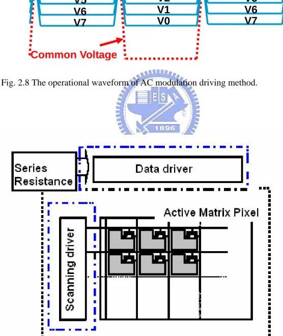
Liquid crystal molecules will be defected under a fixed voltage in a long period. Although the fixed voltage has vanished, the characteristic of the liquid crystals will be destroyed and the twist of liquid crystals can not change with electric field. Therefore, the electric field should be recovered every period to avoid the destruction of liquid crystals. When the frame picture is kept on the same gray level, the electric field across liquid crystals is divided into two electrodes — positive electrode and negative electrode. As electric field is higher than common mode voltage the electrode is called positive electrode, otherwise it is called negative electrode. By this way, the liquid crystal molecules will avoid defection in the fixed electric field. In term of above description, LCD panel can be principally composed of four types —
Chapter 2 7 7 frame inversion, row inversion, column inversion, and dot inversion. They are listed in Fig. 2.6. Frame inversion is that all the adjacent pixels of the LCD panel have the same electrode. Row inversion and column inversion is that each adjacent column pixel and adjacent row pixel have the same electrode respectively. Finally, all the adjacent pixels of LCD panel have different electrode is called dot inversion. Dot inversion is the major driving method of LCD panel. By the opposite polarity of the voltage vertically and horizontally side by side to each pixel, dot inversion can reduce clustered DC voltage in the screen which may result image sticking and to reduce the screen flickering. No matter what methods the LCD panel will be driven, all the pixels will change polarity on the frequency of 60 Hz (16ms). In other word, the polarity of each pixel is alternating changed.
Based on the operational type of common mode voltage, the driving method can also be classified into direct driving and AC modulation driving. They are shown in Fig. 2.7 and Fig. 2.8 respectively. Direct driving method would keep its common voltage on a constant level. But, the common mode voltage of AC modulation driving method would change its polarity in turns. The characteristics of two driving methods are listed below:
Direct driving method:
– Frame, row, column, and dot inversion are all available. – Crosstalk and flicker can be eliminated.
z AC modulation driving method:
– Frame and row inversion are available. – Low power dissipation in data driver.
Chapter 2 8 8 The periphery circuit blocks of LCD panel are composed of four parts — display panel, timing controller, scan driver and data driver. In Fig. 2.9 is the block diagram of the LCD panel driver circuits. Display panel is constructed of active matrixes and its structure layout is illustrated in the Fig. 2.10. The active matrixes are similar to DRAM (dynamic random access memory) which is used to charge and discharge the capacitor on the pixels. Timing controller is responsible for transiting RGB (red, green, and blue) signals to the data driver and controlling the behavior of scan driver. As soon as one voltage level of the scan lines rises, the RGB signals will be transited through the data driver. After a period, the voltage level of this scan line will be disabled and next scan line will act. All voltage levels of those scan lines will change in turn. As for scan driver and data driver, they will be further discussed in the following sections.
2.3.1 Scan Driver Circuit
Scan driver, shown in Fig. 2.11, consists of shifter register, level shifter, and output buffer. Shifter register is used to store digital input signals and transit them to the next stage according to timing clock. Because the turn-on voltage of active pixels is high, scan driver should drive the active pixels with a high voltage. The purpose of the level shifter is to convert the digital signals to a higher level voltage. Finally, since the scan lines can be modeled as RC (resister and capacitor) ladder shown in Fig 2.12, the output buffer should be used in the last stage. The output buffer is composed of inverter chain. The number of stages employed in the inverter chain depends on the RC ladder.
Chapter 2 9 9 Data driver, shown in Fig. 2.13, mainly contains shifter register, data latch, level shifter, digital to analog converter and output buffer. Furthermore, the first three parts classify as digital architectures. The other two parts belong to analog architectures. Shifter register and data latch manage to transit and store the RGB signals. Also, the purpose of level shifter is the same as the one in scan driver. It is applied to translate the RGB signal to a higher level voltage. As implied by the name, digital to analog converter is used convert the digital RGB signal to analog gray level. Its structures can be divided into many types, and there will be much more detailed discussion in the following chapters. As for output buffer, its purpose is applied to drive active pixels into a desired gray level. The LCD panel usually has large loading, especially in larger panel display or higher resolution display. For this reason, the output buffer should enhance its own charge capability. The corresponding output buffer circuit will be described in the next chapter.
Chapter 2 10 10
Temperature Solid
crystalline Liquid
Nematic
Liquid crystal mesophases
Melting point Clearing point
Fig. 2.1 Phase variation of liquid crystal in different temperature.
T
V
100%
90%
10%
V
90TN
V
100TN
V
90STN
V
100STN
Chapter 2 11 11 Bottom Polarizer Top Polarizer Scan Line Data Line ITO Electrode Color Filter Color Filter Glass
TFT Glass
Light
Pixel
Fig. 2.3 Cross section of LCD module.
Fig. 2.4 The liquid crystal operates in normally white case: (a) light can pass and (b) light is blocked.
Chapter 2 12 12
Fig. 2.5(a) The relationship between digital input codes and input voltage across liquid crystals and (b) the smooth curve between digital input codes and light transmission rate.
1
2
3
4
5
1
2
3
4
5
6
1
2
3
4
5
1
2
3
4
5
6
Frame inversion
1
2
3
4
5
1
2
3
4
5
6
1
2
3
4
5
1
2
3
4
5
6
(N)th Frame
(N+1)th Frame
Row inversion
Chapter 2 13 13
1
2
3
4
5
1
2
3
4
5
6
1
2
3
4
5
1
2
3
4
5
6
Column inversion
1
2
3
4
5
1
2
3
4
5
6
1
2
3
4
5
1
2
3
4
5
6
(N)th Frame
(N+1)th Frame
Dot inversion
Fig. 2.6 Inversion of LCD panel.
Fig. 2.7 The operational waveform of direct driving method.
V0
V1
V2
V3
V4
V5
V6
V7
Gray Scale Voltage
V0
V1
V2
V3
V4
V5
V6
V7
V7
V6
V5
V4
V3
V2
V1
V0
Common Voltage
Chapter 2 14 14
Fig. 2.8 The operational waveform of AC modulation driving method.
Fig. 2.9 Block diagram of the LCD panel driver circuits.
V0
V1
V2
V3
V4
V5
V6
V7
V3
V2
V1
V0
V7
V6
V5
V4
V3
V2
V1
V0
V7
V6
V5
V4
Common Voltage
Chapter 2 15 15
Fig. 2.10 The pixel layout structure of active matrix cell on LCD panel.
Chapter 2 16 16
R
L1C
L1R
L2C
L2R
L3C
L3R
L4C
L4R
L5C
L5Fig. 2.12 RC (resister and capacitor) ladder of scanning line.
Chapter 3 17
CHAPTER 3
OUTPUT BUFFER WITH THRESHOLD
VOLTAGE COMPENSATION
3.1 Design Consideration of Output Buffer for LCD
As LCD panel has come into wide use in portable system, such as notebook computer, there is a big demand of developing low power dissipation, high resolution, high speed and large output swing LCD driver. The detailed architecture of LCD driver has been discussed in the last chapter. They include shifter registers, level shifters, DAC, output buffer, etc. Output buffer is much critical to achieve high speed driving, high resolution, low power dissipation and large output swing. In this thesis some output buffers will be proposed to fit the aforementioned concerns.
Furthermore, take the data sheet of KS0625 in Samsung Corp. as reference, some design specifications will be decided in this thesis. For example, the full swing of output voltage in data driver is ±4 V, and the resolution of DAC has 6-to-64 gray level. Besides, the operational frequency is 50 kHz which is applied for XGA (extended graphic array) resolution. And Table I, gives some examples about operational frequencies for typical (frame rate is 60 kHz) display resolution. The loading in this data sheet is a RC ladder whose value and structure are both illustrated in Fig. 3.1. Finally, due to the serious drift of VTH (threshold voltage) in LTPS technology, some output buffers with VTH compensation will also be designed and discussed to overcome the drift of VTH.
Chapter 3 18
3.1.1 Rail-to-Rail Operational Amplifier
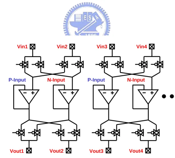
In order to get the large output swing, a rail-to-rail operational amplifier is employed to achieve this purpose [5]-[6]. Make the use of dot inversion driving characteristic in LCD panel; an elegant and lower power rail-to-rail amplifier is proposed which is shown in Fig. 3.2. A PMOS input differential amplifier has a large discharge capability and a NMOS input differential amplifier has a large charge capability. In a dot inversion method; a negative-to-positive or positive-to-negative voltage with respect to the fixed voltage of the backside electrode is driven from the column driver with alternating polarities between column lines. When the column lines are under the negative polarity, electrodes are connected to the outputs of PMOS input differential amplifiers. As the column lines are alternated to the positive polarity, the NMOS differential input amplifiers drive the electrodes to higher level. In brief, the PMOS input differential amplifiers, which have a good discharge capability, drive the negative-going transitions and the NMOS input differential amplifiers, which have a good charge capability, drive the positive-going transitions. So, the common mode input voltage of the PMOS input differential amplifier can be very low and vice versa for the NMOS input differential amplifier. In summary, a large output swing and low power output buffer is achieved by this method.
3.1.2 High Slew Rate Operational Amplifier
Due to the large output loading and timing limit of LCD panel, the slew rate of output buffer in data driver must be enhanced. Fig. 3.3 is a fundamental circuit structure of slew rate enhancement. As shown in this circuit, Amplifier-C monitors the output voltage of first stage amplifier. Then, the voltage of this output is converted to current by the V-I (voltage to current) converter, and the converted current will be
Chapter 3 19
added to the bias current of first stage. By this way, the slew rate of this operational amplifier will be enhanced significantly.
3.2 Slew Rate Enhancement Output Buffer
As previously discussed, a simple operational amplifier with slew rate enhancement in LTPS technology is proposed in Fig. 3.4. For an output buffer, the output is connected to the inverting input (in-) and the input signal is applied to the non-inverting terminal (in+). The differential pair M5-M6, which is biased by a constant current source M1-M4, is actively loaded by the current mirror formed by M7 and M8. Besides, M9 and M10 form a common source output stage and the loading in the output is 680pF. When the output stage of M9-M10 is used to drive a large capacitive load of a LCD panel under a step wise input, it will have a better fall time but a poor rising time since M9 is controlled by a constant current which provides limited charging capability to the load. To overcome this problem, M11–M12, which forms a current comparator and a charging transistor M13 are added. The width and length of M12 is chosen the same as those of M7 and M8 to draw the same amount of current, I/2, where I is the biasing current of the input differential stage. However, the width and length of M11 is chosen to be a little bit larger than half of M4.
(W/L)11 = 1/2(W/L)4 + ∆(W/L) (3-1)
In the stable state with no input signal, the output voltage will equal to the input voltage. The current flowing in M5, M6, M7, M8, and M12 are all I/2. At this
Chapter 3 20
moment, the current flowing in M11 is also I/2. However, since the aspect ratio of M11 is designed to be greater than half of M4, this will force M11 go out of the saturation region and be in the triode region. As a result, the gate voltage of M13 will be forced to be close to the value of VDD. M13 will then stay at “off”. That is, when no input signal is applied, M13 is cut off from the output.
When the input voltage of the non-inverting terminal is raised by a step voltage ∆V1, the current in M5 will be increased to I/2 + (1/2)gm∆V1 but the current in M6 will be decreased to I/2 – (1/2)gm∆V1, where gm is the trans-conductance of M5 and M6.
ID5 = I/2 + (1/2)gm∆V1 (3-2)
ID6 = I/2 – (1/2)gm∆V1 (3-3)
gm = [I(W/L)5µPCox]1/2 (3-4)
µP andCox are the mobility in the p channel and the gate oxide capacitor per unit area, respectively. If ID5 is greater than I/2 + ∆I, it will get the formula which is shown as follow:
∆V1 > 2∆I/gm (3-5)
∆I = 1/2µPCox∆(W/L)(VGS11 – VTHP)2 (3-6)
That is, transistor M11 will go into the saturation region and the gate voltage of M13 will decrease to turn on M13. So, M13 begins to charge the output terminal. The larger varies in ∆V1, the more M13 will be turned on. Since VGS13 can reach a value of VDD, the gate voltage of M13 can be decreased to a really low and M13 can be turned to fully “on” to charge the output terminal by a maximal speed. When the
Chapter 3 21
output voltage reaches to the level that the voltage difference between the input and output is less than 2∆I/gm, M13 will stop to charge the output terminal. By this way, the output buffer can be used to drive a larger capacitive load. Furthermore, the driving capability can be improved by increasing the size of M13, M9, and M10. But, there is one thing must be noticed. Increasing the aspect ratio of M13 does not increase the static current; however, increasing the sizes of M9 and M10 will increase the static current. In other ward, that will increase the total power consumption.
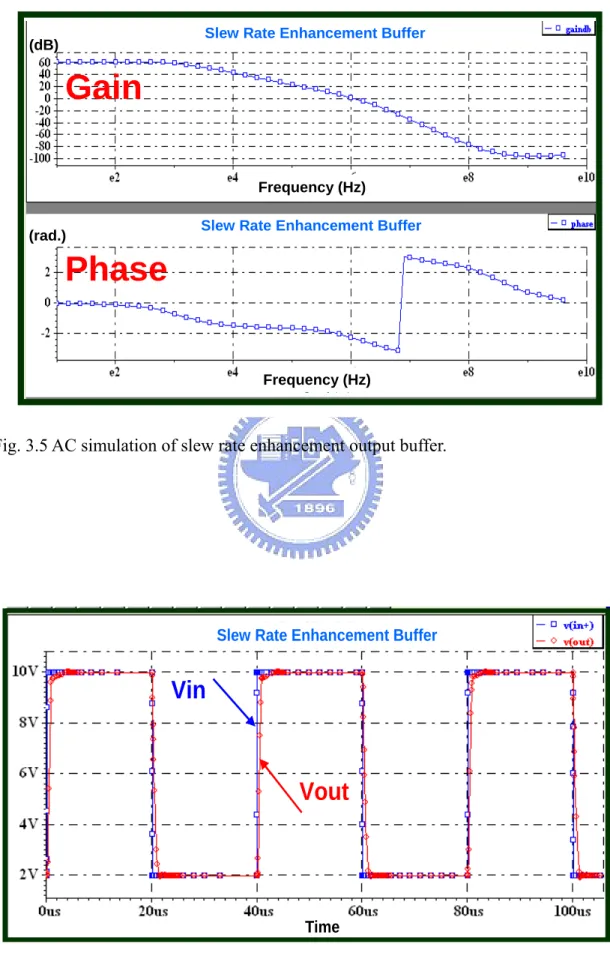
The simulation results of frequency response in TOPPOLY 6-µm LTPS model are shown in Fig. 3.5. It can find that open loop gain is 61.5 dB, unit gain frequency is 2.1 MHz, and the phase margin is 53.9°. Fig. 3.6 shows the output waveform when input signal is applied. The input signal swing is 2V-10V and operational frequency is 50 kHz. Besides, the rising and falling time of output waveform are 1.58 µs and 1.40 µs, respectively. In summary, the specification of this output buffer is listed in Table II. Fig. 3.7 is the whole layout of this circuit in TOPPOLY 6-µm LTPS process.
3.3 Low Power Class-B Output Buffer
3.3.1 Design Conception
According to the above circuit, it can drive heavy loading by slew rate enhancement structure, but there is still a lot to be improved in terms of power consumption. In this section a low power class-B output buffer is included and implemented in TOPPOLY 6-µm LTPS process [7]-[9]. Fig. 3.8 is the whole operational amplifier circuit diagram and its own loading is also shown in this figure. The loading also take the data sheet of KS0625 in Samsung Corp. as a reference. As an output buffer, the output is connected to the inverting input (in-) and the input signal is applied to the non-inverting terminal (in+). This output buffer is composed
Chapter 3 22
of a differential stage (M4-M8), two comparators (M9-M12), and a push-pull output stage (M13-M14). The differential pair M5-M6, which is biased by the constant current source M1-M4, is loaded by the diode-connected transistors M7 and M8. The comparators are used to sense and amplify the voltage difference of two inputs. Then the output of the comparators turns on or off the push-pull transistors. The aspect ratios of M9 and M11 are chosen to be the same as those of M7 and M8. However, the W/L of M10 is chosen to be a little bit larger than half of M4 but M12 a little bit smaller than half of M4.
(W/L)10 = 1/2(W/L)4 + ∆(W/L) (3-7)
(W/L)12 = 1/2(W/L)4 – ∆(W/L) (3-8)
In the stable state with no input signal, the output voltage will equal to the input voltage. The current flowing in M5, M6, M7, M8, M9 and M11 are all I/2. Then, the current flowing in M10 and M12 are also I/2. However, since the aspect ratio of M10 is designed to be greater than half of M4, this will make M10 go out of the saturation region and be in the triode region. So, the gate voltage of M14 will be forced to be close to the value of GND. M14 will then stay at “off”. For the comparator M11-M12, similarly, M11 will be in the triode region. The gate voltage of M13 will be forced to be close to the value of VDD. M13 will also stay at “off’. That is, when no input is applied, M13 and M14 are almost cut off from the output. However, when the input voltage of the non-inverting terminal is raised by a step voltage ∆V1, the current in M5 will be increased to I/2 + (1/2)gm∆V1, but the current in M6 will be decreased to I/2 – (1/2)gm∆V1, where gm is the trans-conductance of M5 and M6. And all of these are list in formula (3-9), (3-10), and (3-11).
Chapter 3 23
ID5 = I/2 + (1/2)gm∆V1 (3-9)
ID6 = I/2 – (1/2)gm∆V1 (3-10)
gm = [I(W/L)5µnCox]1/2 (3-11)
µn andCox are the mobility in the n channel and the gate oxide capacitor per unit area, respectively. The current in M6 is mirrored by M8, M9, and M11 to the two comparators M9-M12. Since ID6 is decreased, M10 will still stay in the triode region. M14 will than still stay at “off”. However, if ID6 is smaller than I/2 + ∆I, it will get the formula which is shown as follow:
∆V1 > 2∆I/gm (3-12)
∆I = 1/2µnCox∆(W/L)(VGS4 – VTHP)2 (3-13)
That is, transistor M11 will go into the saturation region and its drain voltage will decrease to turn on M13. Then, M13 begins to charge the output node. The larger varies in ∆V1, the more M13 is turned on. Since the gate voltage of M13 can be decreased to a really low and M13 can be turned to almost “on” to charge the output by a maximal speed. Hence, the output transistors M13-M14 can be designed to be of smaller sizes than the conventional output buffer. When the output voltage reaches the level that the voltage difference between the input and output is less than 2∆I/gm, VGS13 will be reduced and M13 begins to stop charging the output node. The smaller voltage varies, the more M13 is turned off. Similarly, when the input voltage of the non-inverting input is reduced by a step voltage ∆V1 from the stable state, M13 will still stay at “off”. If ∆V1 is greater than 2∆I/gm, M10 will go into the saturation region and M14 starts to discharge the output node. Also, when the output voltage reaches the level that the voltage difference between the input and output is less than 2∆I/gm,
Chapter 3 24
M14 begins to stop discharging output node. Hence, with the consideration of the offset voltage, the operation of this buffer can be summarized as follow:
z When Vin – Vout – Vos > 2∆I/gm, M13 will charge the output node. z When Vin – Vout – Vos < –2∆/Igm, M14 will charge the output node.
z When –2∆/Igm < Vin – Vout – Vos < 2∆Igm, both output transistors stay at off.
Where Vos is the input offset voltage of the output buffer. Since transistor M13 and M14 are almost “off” at the stable state, they consume almost no current. That is why this architecture of output buffer is low power while the operational speed can maintain relatively high.
3.3.2 Measurement Result
Based on lower power considerations, a low power class-B output buffer is proposed and implement in TOPPOLY 6-µm LTPS process. Furthermore, the simulation results of frequency response in TOPPOLY 6-µm LTPS model are shown in Fig. 3.9. It can find that open loop gain is 40 dB, unit gain frequency is 1.7 MHz, and the phase margin is 73.8°. Fig. 3.10 shows the output waveform when input signal is applied. The input signal swing is 2V-10V and operational frequency is 50 kHz. Besides, the rising and falling time of output waveform are 2.88 µs and 3.30 µs, respectively. In summary, the specification of this output buffer is listed in Table III.
Fig. 3.11 is the whole layout of this circuit in TOPPOLY 6-µm LTPS process. Also, the measurement environment and glass photo are shown in Fig. 3.12. The input pattern and DC bias are generated by pulse generation and power supply through probe station. Besides, the output waveform is also investigated by oscilloscope through probe station. The total instruments for measuring class-B output buffer are
Chapter 3 25
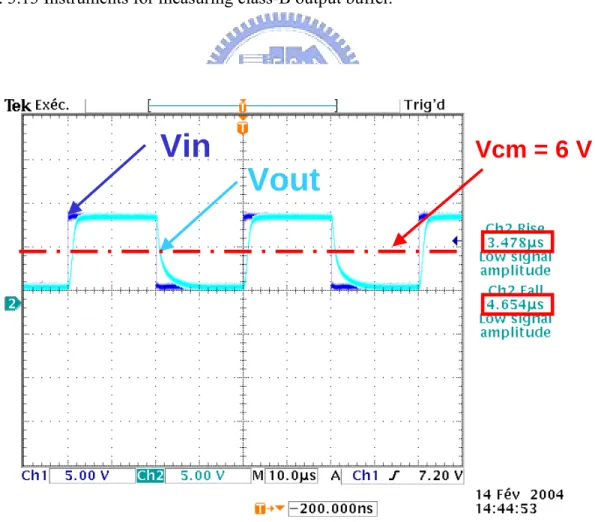
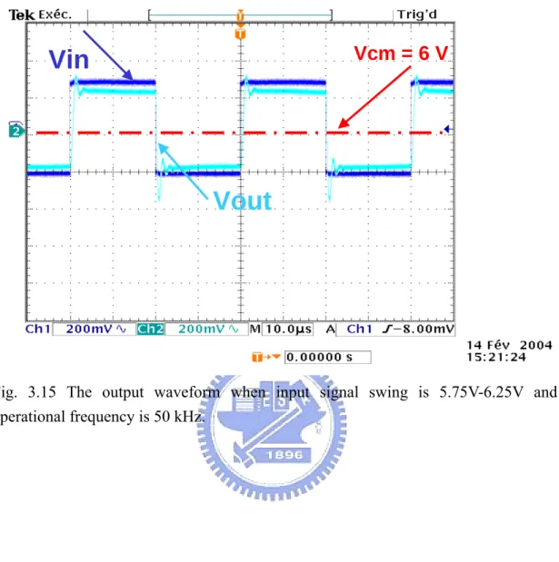
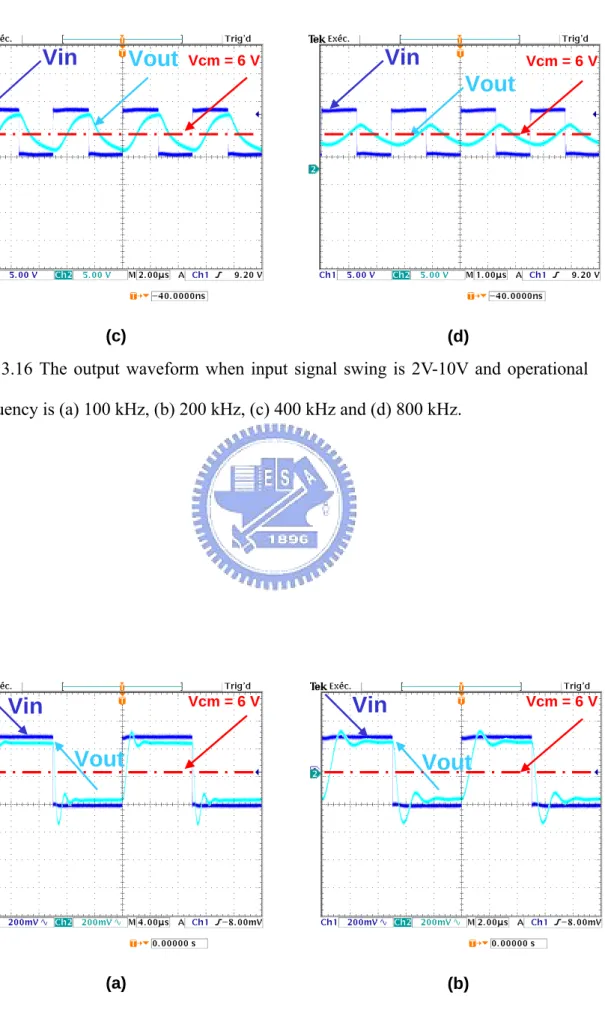
illustrated in Fig. 3.13. According to above descriptions, the performance of this circuit are measured and list below. Fig. 3.14 is the waveform when input signal swing is 2V-10V and operational frequency is 50 kHz. In this figure, it can see that the rising time and falling time are 3.478 µs and 4.654 µs. These results are a little different from the simulation. About this different, it may be caused by the drift VTH, and this problem will be solve in next section. But the function of this class-B output buffer is work in general. Besides, the output waveform is also shown in Fig. 3.15 when input signal swing is 5.75V-6.25V and operational frequency is 50 kHz. It can see that the output waveform has a little overshot in rising and falling step. These results are caused by the phase margin and it also shows the relationship between phase margin and overshot in Table IV. Furthermore, the output waveform when input signal swing is 2V-10V and operational frequency is 100 kHz, 200 kHz, 400 kHz and 800 kHz is also measured and shown in Fig. 3.16(a), Fig. 3.16(b), Fig. 3.16(c), and Fig. 3.16(d). As it can see, when input operational frequency is fewer than 400 kHz, the output waveform can reach the full swing in 20 µs. In addition, Fig. 3.17(a), Fig. 3.17(b), Fig. 3.17(c), and Fig. 3.17(d) are the output waveform when input signal swing is 5.75V-6.25V and operational frequency is 100 kHz, 200 kHz, 400 kHz and 800 kHz. It also shows that, the output waveform can function well when input signal operational frequency is fewer than 400 kHz. In summary, it can announce that this class-B output buffer in TOPPOLY 6-µm LTPS process can operate upper to 400 kHz. Furthermore, it will not consume extra power when input signal is stable.
3.4 Output Buffer with V
THCompensation
3.4.1 The Causation of Offset Voltage
Chapter 3 26
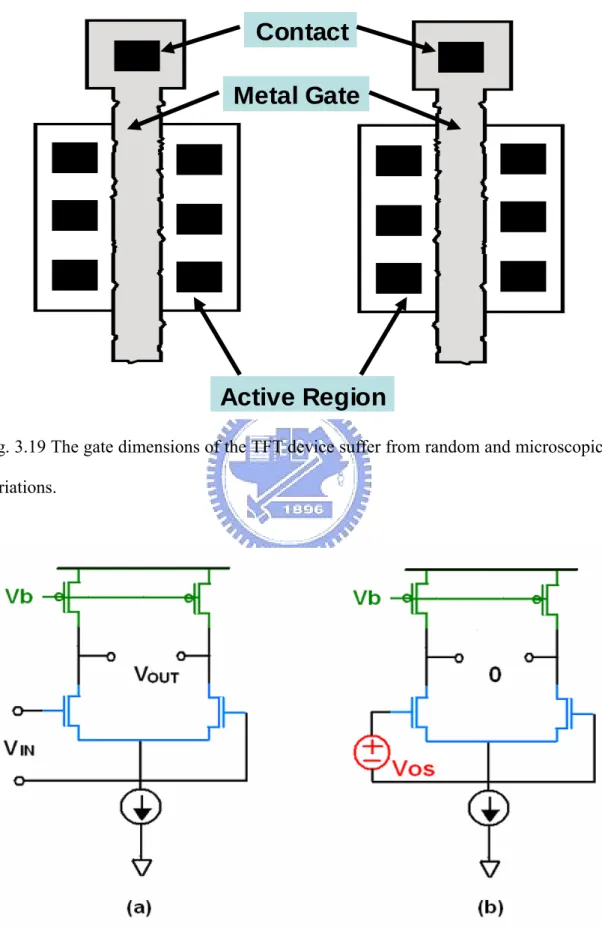
digital assistant) as well as notebook computers, data driver which are integrated in TFT (thin film transistor) have recently been developed to reduce cost and complexity in manufacture. As what is showed in Fig. 3.18, analog output buffer is the major circuit block for the data driver in TFT-LCD. It can amplify the input analog signal because the signal may be too small to drive a load. And, the operational amplifier is considered as analog output buffer because the operational amplifier has rather low linearity error, wide output range and high driving capability. Therefore, it should be urgently realized on glass in LTPS technology. However, the device in LTPS technology has serious problems for analog output buffer such as kink effect and dramatic variation of threshold voltage.
It should be noted that the mismatch of device in LTPS technology results in the output variation. For example, a finite mismatch is due to the uncertainties in each step of the manufacturing process. As shown in Fig. 3.19, the gate dimensions of the TFT device suffer from random and microscopic variations; hence mismatches exists between the equivalent lengths and widths of two transistors that are identically laid out. Besides, the TFT device has the large varied characteristics such as mobility and threshold voltage. These variations vary randomly from one device to another. And the offset voltage in output is increased when the variation of threshold voltage is serious. Express the characteristics of a TFT device in saturation region as ID = (1/2)µCOX(W/L)(VGS-VTH)2, it can be observed that mismatches between µ, COX, W, L and VTH result in mismatch between drain currents (for a given VGS) or gate-source voltages (for a given drain current) of two nominally-identical transistors. Consider the conventional operational amplifier without offset cancellation shown in Fig. 3.20(a). With VIN = 0 and perfect symmetry, VOUT = 0, while in the presence of mismatches, VOUT ≠ 0. As shown in Fig. 3.20(b), the circuit suffers from an offset voltage equal to the observed value of VOUT when VIN is set to zero. In practice, it is
Chapter 3 27
more meaningful to specify the offset voltage in input, defined as the input level that forces the output voltage to go to zero. According to the above description, the conventional operational amplifier without offset cancellation of Fig. 3.20(a) is to amplify a small input voltage. Then, as depicted in Fig. 3.21, the output contains amplified replicas of both the signal and offset voltage. And, if the offset voltage is serious, the offset voltage in output will force the conventional operational amplifier falls into nonlinear operation.
To calculate the offset voltage of the conventional operational amplifier without offset cancellation, Fig. 3.20(a) is be modified as Fig. 3.21. The offset voltage of N-type TFT device and P-type TFT device is inserted in Fig. 3.21. If ID1 = ID2 and ID3 = ID4, then a formula of input offset voltage is shown below.
VOS,N = [(VGS-VTH)N/2][∆(W/L)/(W/L)]N + ∆VTH,N (3-14)
VOS,P = [(|VGS-VTH|)P/2][∆(W/L)/(W/L)]P + ∆VTH,P (3-15)
Besides, VOS,P is amplified by a gain of gmP(rON || rOP) and divided by gmN(rON || rOP) when referred to the main input. Then, according to formula (3-14) and (3-15), a total offset voltage referred to the main input can be calculated in following formula.
VOS,IN = { [(|VGS-VTH|)P/2][∆(W/L)/(W/L)]P + ∆VTH,P }( gmP/ gmN)
+ [(VGS-VTH)N/2][∆(W/L)/(W/L)]N + ∆VTH,N (3-16)
As previously described, the offset voltage caused by P-type TFT device can be decreased by enlarging the size of N-type TFT device. In addition, the offset voltage caused by the mismatch and random variation of the N-type TFT device can be eliminated by adopting common centroid layout. Furthermore, the offset voltage
Chapter 3 28
caused by the latter gain stage can also be improved, because it will be divided by the gain of first stage. Therefore, if the variation of threshold voltage caused by the N-type TFT device can be minimized, the operational amplifier can function well and has rather low linearity error.
According to the above discussion, if the analog output buffer can be designed more elegant to eliminate the offset voltage, the data driver can be integrated on glass in LTPS technology promisingly. Thus, this thesis aims to propose some new analog output buffers with threshold voltage compensation. An AZ (auto zeroing) method was employed to reduce the offset voltage and it can process the higher resolution and higher quality panel.
3.4.2 Design of Output Buffer with V
THCompensation
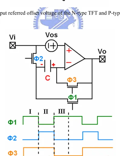
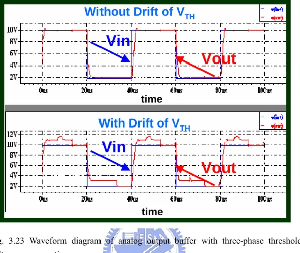
The basic idea of auto zeroing method is sampling the unwanted input offset voltage and then subtracting it from the instantaneous value of contaminated signal at the input [10]. A three-phase auto zeroing method using to reduce the offset voltage is shown in Fig. 3.22. The operational amplifier is employed class-B structure which is discussed in last section. The offset voltage of the operational amplifier is reduced as follow. During the first phase (φ1), the offset-holding capacitor C is reset by the output of the amplifier. Then, during the second phase (φ2), the offset voltage is detected in the output voltage and hold by capacitor C. Finally, during third phase (φ3), the detected offset voltage is added to the amplifier input, completing the offset cancellation. The output waveform of the three phase threshold voltage compensation which is simulated with TOPPOLY 6-µm LTPS model shows in Fig. 3.23. Through this sequence, the offset-holding capacitor C is pre-charged by the operational amplifier and finally compensates the offset voltage caused by the variation of
Chapter 3 29
threshold voltage in TFT device. In additional, Fig. 3.24 is the layout diagram in TOPPOLY 6-µm LTPS process.
According to the discussion above, the analog output buffer must has three phases to complete the threshold voltage compensation. It will limit the operational speed of output buffer. For this reason, if the phases for threshold voltage compensation can be reduced, the operational speed for analog output buffer can be enhanced further. Besides, it will be more promising to process the higher resolution and higher quality panel. So, a two-phase output buffer is proposed and shown in Fig. 3.25 to improve above drawbacks. As shown in this circuit architecture, Vcm is the common mode voltage of the data driver, and C is the offset-holding capacitor. During the first phase (φ1), the offset voltage is detected in the output terminal and hold by capacitor C. Then, VO(φ1) = Vcm + VOS(φ1) and VC(φ1) = VOS(φ1). During the second phase (φ2) the detected offset voltage is added to the amplifier input, and completes the offset cancellation. So, VO(φ2) = Vi + [VOS(φ2) – VOS(φ1)] and VC(φ2) = VOS(φ1). From the above description, the analog output buffer only needs two phases to complete the threshold voltage compensation. The output waveform of the two-phase threshold voltage compensation simulated with TOPPOLY 6-µm LTPS model is shown in Fig. 3.26. Fig. 3.27 is the full layout in TOPPOLY 6-µm LTPS process. As a result, the analog output buffer will have a better immunity to the variation of the threshold voltage. Furthermore, a more advance analysis is also done in this thesis. By modifying the VTH in TFT model, it can observe the output variation in output buffer. As describe above chapter, if a 64 gray level data driver must be implemented, the output variation must less than 1/2 LSB (last significant bit). In other word, if the output swing in output buffer is ±4 V, the output variation must less than 32 mV to fit above demands. Fig. 3.28 (Vi = 10 V) and Fig. 3.29 (Vi = 2 V) show the relationship between VTH and output variation in output buffer. It can see that, if
Chapter 3 30
the drift VTH in transistors M5-M8 and M13-M14 are less than 0.6 V (42.8%), the variation in output can be controlled under 32 mV.
Besides, a secondary analog output buffer with modified two-phase threshold voltage compensation is also designed and shown in Fig. 3.30. This structure only needs two phases to complete the threshold voltage compensation, too. What more important is that it does not need the extra common mode voltage (Vcm). Similarly, during the first phase (φ1), the offset voltage is detected in the output terminal and hold by capacitor C. Then, VO(φ1) = Vi + VOS(φ1) and VC(φ1) = VOS(φ1). During the second phase (φ2) the detected offset voltage is added to the amplifier input, and completes the offset cancellation. So, VO(φ2) = Vi + [VOS(φ2) – VOS(φ1)] and VC(φ2) = VOS(φ1). However, this structure is simulated in TOPPOLY 3-µm LTPS model. The simulated waveform is shown in Fig. 3.31. Fig. 3.32 is the full layout diagram of this circuit in TOPPOLY 3-µm LTPS process. Also, a more advanced analysis is done in this circuit. By modifying the VTH in TFT model, it can observe the output variation in output buffer. Because the output swing in this output buffer is ±3V, the output variation must less than 23 mV to fit above regulation. Fig. 3.33 (Vi = 8 V) and Fig. 3.34 (Vi = 2 V) show the relationship between VTH and output variation in output buffer. It can see that, if the drift VTH in transistors M5-M8 and M13-M14 are less than 0.6V (48.3%), the variation in output can be controlled under 23 mV.
In summary, this invention of analog output buffer with threshold voltage compensation can be applied in the data drivers for LCD panel system. By employing the threshold voltage compensation method, the analog output buffer can overcome the variation of threshold voltage. Besides, output buffer will be more promising to be integrated in the higher resolution and higher quality LCD panel.
Chapter 3 31
Table I
Operation frequencies specification of LCD panel.
Resolution VGA SVGA XGA SXGA UXGA
Total
800×525 1056×628 1344×806 1688×1066 2160×1250Active
640×480 800×600 1024×768 1280×1024 1600×1200Frame Rate
60 Hz 60 Hz 60 Hz 60 Hz 60 HzFr (row rate)
31.46 KHz 37.87 KHz 48.36 KHz 63.98 KHz 75.00 KHzFp (pixel rate)
25 MHz 40 MHz 65 MHz 108 MHz 162 MHzRow Period
31.78 µs 26.40 µs 20.68 µs 16.63 µs 13.33 µs Table IISpecification of slew rate enhancement output buffer.
Output Buffer
Specification
Operational Frequency
50 kHzGain
61.5 dBPhase Margin
53.9°Unit Gain Frequency
2.1 MHzDynamic Range
2 V – 10 VRising Time
1.58 µsFalling Time
1.40 µsChapter 3 32
Table III
Specification of Class-B output buffer.
Output Buffer
Specification
Operational Frequency
50 kHzGain
40 dBPhase Margin
73.8°Unit Gain Frequency
1.7 MHzDynamic Range
2 V – 10 VRising Time
2.88 µsFalling Time
3.30 µsPower Consumption
1.6 mWTable IV
The relationship between phase margin and overshot.
Phase Margin
Wu/W2
Overshoot
45°
1.000 36.8%55°
0.700 13.3%60°
0.577 8.7%65°
0.466 4.7%70°
0.364 1.4%75°
0.268 0.008%Chapter 3 33
Load
5 k
Ω
5 k
Ω
10 k
Ω
10 k
Ω
10 k
Ω
10 k
Ω
25 pF
25 pF
25 pF
Vout
Vcm
Fig. 3.1 The values of RC ladder in Samsung data sheet.
Vin1 Vin2 Vout2 Vout1 Vin3 Vin4 Vout4 Vout3
P-Input N-Input P-Input N-Input
Chapter 3 34
Fig. 3.3 A fundamental circuit structure of slew rate enhancement.
M1 M2 M3 M4 M11 M9 M5 M6 M7 M8 M12 M10 R C
CL = 680 pF
Vin- Vin+ Vout M13Chapter 3 35
Gain
Phase
Frequency (Hz)
Frequency (Hz)
Slew Rate Enhancement Buffer
Slew Rate Enhancement Buffer
(dB)
(rad.)
Fig. 3.5 AC simulation of slew rate enhancement output buffer.
Vin
Vout
Time
Slew Rate Enhancement Buffer
Chapter 3 36
vdd
in
out
vb
gnd
Fig. 3.7 Layout of slew rate enhancement output buffer.
Comparator
M1Vin-Vin+
Vout
R1 C1 R2 C2 M2 M3 M7 M8 M5 M6 M9 M11 M13 M4 M10 M12 M14Load
5 kΩ 5 kΩ 10 kΩ 10 kΩ 10 kΩ 10 kΩ 25 pF 25 pF 25 pF Vout VcmChapter 3 37
Gain
Phase
Low-Power High-Speed Class-B Buffer
Low-Power High-Speed Class-B Buffer
Frequency (Hz)
Frequency (Hz) (dB)
(rad.)
Fig. 3.9 AC simulation of class-B output buffer.
Vin
Vout
Low-Power High-Speed Class-B Buffer
time
Chapter 3 38
in
vb
gnd
vcm
out
vdd
Load
Fig. 3.11 Layout of class-B output buffer.
Fig. 3.12 The input pattern and DC bias are generated by pulse generation and power supply through probe station.
in gnd vcm vdd out
Probe Station
Chapter 3 39
Fig. 3.13 Instruments for measuring class-B output buffer.
Vin
Vout
Vcm = 6 V
Fig. 3.14 The output waveform when input signal swing is 2V-10V and operational frequency is 50 kHz.
Agilent 81110A Tektronix TDS 3054B
Chapter 3 40
Vin
Vout
Vcm = 6 V
Fig. 3.15 The output waveform when input signal swing is 5.75V-6.25V and operational frequency is 50 kHz. (a)
Vin
Vout
Vin
Vout
(b) Vcm = 6 V Vcm = 6 VChapter 3 41
(c) (d)
Vin
Vout
Vin
Vout
Vcm = 6 V Vcm = 6 V
Fig. 3.16 The output waveform when input signal swing is 2V-10V and operational frequency is (a) 100 kHz, (b) 200 kHz, (c) 400 kHz and (d) 800 kHz.
(a) (b)
Vin
Vout
Vin
Vout
Vcm = 6 V Vcm = 6 VChapter 3 42 (c) (d)
Vin
Vout
Vin
Vout
Vcm = 6 V Vcm = 6 VFig. 3.17 The output waveform when input signal swing is 5.75V-6.25V and operational frequency is (a) 100 kHz, (b) 200 kHz, (c) 400 kHz and (d) 800 kHz.
Chapter 3 43
Metal Gate
Active Region
Contact
Fig. 3.19 The gate dimensions of the TFT device suffer from random and microscopic variations.
Fig. 3.20(a) The conventional operational amplifier with offset voltage measured at the output, (b) circuit of (a) with its offset voltage referred to the input.
Chapter 3 44
Fig. 3.21 The input referred offset voltage of the N-type TFT and P-type TFT.
Fig. 3.22 Circuit diagram of analog output buffer with three-phase threshold voltage compensation.
Chapter 3 45
Vout
Vin
Vout
Without Drift of V
THtime
time
Vin
With Drift of V
THFig. 3.23 Waveform diagram of analog output buffer with three-phase threshold voltage compensation.
vb
gnd
vdd
Vi
Vo
Φ1
Φ2
Φ3
Φ1b
Φ3
Chapter 3 46
Fig. 3.25 Circuit diagram of analog output buffer with two-phase threshold voltage compensation.
Vin
Vout
Vin
Vout
time
time
Without Drift of V
THWith Drift of V
THFig. 3.26 Waveform diagram of analog output buffer with two-phase threshold voltage compensation.
Chapter 3 47
vb
gnd
vdd
Vi
Vo
Φ1
Φ2
vcm
Fig. 3.27 Layout of output buffer with two-phase threshold voltage compensation.
Chapter 3 48
Fig. 3.29 The relationship between VTH and output variation when Vin = 2 V.
Fig. 3.30 A secondary analog output buffer with modified two-phase threshold voltage compensation.
Chapter 3 49
Fig. 3.31 Waveform diagram of secondary analog output buffer with modified two-phase threshold voltage compensation.
Fig. 3.32 Layout of secondary analog output buffer with modified two-phase threshold voltage compensation.
Load
in
vb
vdd
out
gnd
s1 s2
300 µm
Vin
Vout
Vin
Vout
Without Drift of Vt
With Drift of Vt
Voffset
time time time
Chapter 3 50
Fig. 3.33 The relationship between VTH and output variation when Vin = 8 V.