複晶矽薄膜電晶體中漏電流及可靠度課題之研究
82
0
0
全文
(2)
(3) 複晶矽薄膜電晶體中漏電流及可靠度課題之研究 研究生:李明賢. 指導教授:. 林鴻志 黃調元. 博士 博士. 國立交通大學 電子工程學系. 電子研究所. 摘要 本論文提出並實作一種具有自我對準能力之複晶矽奈米線薄膜電晶體,以及一種應 用於解析熱載子衰退的新穎測試結構。首先,我們描述奈米線薄膜電晶體之製程,及如 何製作此複晶矽奈米線的製程參數。我們也審視了影響奈米線尺寸及形狀之因子。這個 製程非常簡單,不牽涉到複雜且昂貴的電子束微影或是深紫外光微影設備。 我們研究並討論了奈米線薄膜電晶體的開狀態特性,包括剛製成的元件及經過電漿 處理的元件,然後討論了電漿處理及尺寸對於電特性的影響。與傳統平面結構的元件比 較,此奈米線通道的優點包括有:絕佳的開電流密度及對短通道效應有較佳的控制能力 等等。此外,由於奈米線的寬度很窄,在進行氫化的時候能夠更夠效率地使元件的特性 改善。 我們也研究了奈米線薄膜電晶體其獨特的關狀態漏電流機制。產生於閘極與汲極間 重疊區域的閘極引發汲極漏電流(gate-induced drain leakage, GIDL),被發現是造成此一 異常漏電流的元兇。我們仔細檢驗了此一異常漏電流的產生原因,以及電漿處理對於此 漏電流的影響。我們發現此一電流起因於在閘極與汲極介面的低掺雜區域,此區域引發 了一條額外的漏電流路徑。在檢驗了漏電流的起因之後,我們提出並實際驗證了數種減. i.
(4) 少此一漏電流的方案。這些方案包括了快速熱退火(Rapid thermal annealing, RTA)、在閘 極與汲極間插入一層氮化矽、以及改使用複晶矽鍺材料作為奈米線通道等。這數種方案 的特色被逐一比較並加以討論。 我們也提出並實作了一種新穎的測試結構,可以解析薄膜電晶體中熱載子衰退所發 生的位置及時間演變。此一新穎測試結構的製作方式與傳統的薄膜電晶體一樣容易,與 現在的超大規模積體電路製程完全相容,並且不需要額外的光罩。我們檢視了此一測試 元件所帶來之靈敏度的提昇以及在決定施壓條件時的優點,也探討了金屬後電漿處理對 於熱載子衰退效應的影響。特別的是,我們在研究過程中,利用此一結構發現了兩種會 造成臨界電壓漂移的機制。 由於此測試結構的高靈敏度及解析能力,使得在研究可靠度相關議題時,能夠直接 利用此一測試結構直接觀察元件的衰退現象,不必再利用高電壓施壓條件下的結果,去 推測元件在正常操作或是低電壓施壓條件之下的衰退現象,並可以比較元件在高低電壓 施壓下的不同現象和機制。 我們也利用此一測試結構,研究了當元件操作於交流模式時,所產生的熱載子衰退 現象。關於操作頻率、上升及下降時間都有詳細的探討。利用此一測試結構的特性,輸 入訊號中各個準位階段其所對應到的損傷位置可以被定位出來。實驗結果顯示,損傷主 要是當閘極訊號切換時,瞬間所產生的熱載子所導致。伴隨著偵測熱載子衰退時的高靈 敏度,此一元件也可以應用於一般交流操作時的可靠度研究之用。 在此論文的最後一個部份,我們進行了關於缺陷能態密度的分析。在說明原理及方 式之後,我們可以利用前述的測試元件萃取出當元件受到熱載子損傷之後,其能態密度 分佈的變化。由於傳統元件在受到熱載子損傷後,通道中各部位的能態密度分佈將會變. ii.
(5) 得不均勻,且局部的缺陷密度增加量將會在萃取能態密度分佈時被整體所稀釋,造成實 務上萃取的困難。利用此一測試元件,我們可以萃取出各部位其能態密度分佈的變化, 並重組成元件衰退後的真實分佈狀態,並利用元件模擬技術重現元件的次臨界特性曲 線。 關鍵字:薄膜電晶體;複晶矽;奈米線;自我對準;閘極引發汲極漏電流;電漿處 理;矽鍺;快速熱退火;熱載子;熱載子衰退;熱載子效應;測試結構;交流施壓;能 態密度;元件模擬;可靠度。. iii.
(6)
(7) A Study of Leakage Current and Reliability Issues in Poly-Si Thin-Film Transistors Student: Ming-Hsien Lee. Advisor: Dr. Horng-Chih Lin Dr. Tiao-Yuan Huang. Department of Electronics Engineering & Institute of Electronics National Chiao-Tung University. Abstract In this thesis, we proposed and demonstrated a poly-Si thin-film transistor with self-aligned nanowire channels, as well as a novel test structure suitable for resolving hot-carrier degradation. Firstly, the fabrication of proposed NWTFT was described, followed by the detail in poly-Si nanowire formation and investigation of the factors affecting size and shape of the nanowire. The fabrication is simple and does not involve costly lithography tools. On-state characteristics of NWTFT were then examined and discussed, including as-fabircated and plasma-treated samples. The effects of post-metal treatment and geometric parameters on NWTFT were then discussed. The advantages of NWTFT were demonstrated by comparing with traditional planar structures. Such nanowire structure has been shown to be excellent in terms of on-current per unit width and controllability over short-channel effects. Owing to the fine nano-scale of NW width, hydrogenation would be very efficient for further performance improvement. The unique off-state leakage mechanism of NWTFT was also investigated. A gate-induced drain leakage (GIDL), which is generated in the overlapped region between the gate and the drain, was uncovered as the major culprit for the anomalous leakage. The origin. v.
(8) of the anomalous leakage was then examined, as well as the effect of post-metal treatment. This current was found to originate from the lightly-doped region at gate/drain interface, which induced an additional current path. After that, several modifications were proposed and demonstrated in order to alleviate the unique leakage. Rapid thermal annealing (RTA), inserted nitride mask, and poly Si1-XGeX were investigated and compared. A tester, which can spatially and temporally resolve hot-carrier degradations, was proposed and demonstrated. The fabrication of the novel test structure is simple and compatible with standard ULSI processings without extra masking. Advantages in sensitivity and stress-condition determination were discussed, accompanying with the effects of post-metal plasma treatment on hot-carrier degradations. Specifically, we found that at least two mechanisms are responsible for the negative threshold voltage shift detected by monitor transistors. The high sensitivity and resolving capability of the novel test structure can also help researchers observe directly degradation phenomena occurring when devices are stressed under moderate or minor conditions. We also studied the phenomena of hot-carrier degradation during AC operations using the proposed test structure. Effects of frequency, rising and falling times, were investigated and discussed. The phenomena of the hot-carrier degradation can be spatially resolved using the proposed tester. By applying such a tester to AC hot-carrier stressing, the relationship between different stages of input signal and resultant damage location can be established. The tester also showed a high sensitivity in detecting even mild AC degradation. The experiment provides unambiguous evidence that the damage occurs during the transient stages, with the aid of the test structure. At the last part of the thesis, the analyses related to effective density-of-states distributions were performed. After the description of experimential procedures, effective. vi.
(9) density-of-states distributions of localized damaged regions were extracted using the aforementioned tester. The information revealed by the analyses was then discussed. The extracted density-of-states distributions for both unstressed and stressed films were used to conduct simulations for subthreshold characteristics of TFTs and compared with the experimental data. The combination of the proposed novel test structure and density-of-states extraction technique provides a powerful tool for resolving the non-uniform density-of-states distribution of TFTs after HC stressing, which is impossible using traditional testers. Keyword: Thin-film transistor; Polycrystalline silicon; Poly-Si; Nanowire; NWTFT; Self-aligned; Gate-induced drain leakage (GIDL); Plasma treatment; Silicon germanium; Rapid-thermal annealing (RTA); Hot-carrier; Hot-carrier degradation; Hot-carrier effect; Test structure; HCTFT; AC stress; Density of states; Device simulation; Reliability.. vii.
(10)
(11) 誌. 謝. 首先誠摯地感謝指導教授黃調元博士及林鴻志博士,兩位老師細心的教導使我得以 一窺此一領域的深奧,不時的討論並指點我正確的方向,使我在這些年中獲益匪淺。黃 老師的博學多聞、林博對於研究的嚴謹態度,都是我學習的典範。從提醒我不要把 paper 當聖經,要有批判思考的精神,到指導我發現問題、定義課題、並解決問題的能力與技 巧,老師們的字字句句,學生深感於心。 從碩士班加入當時的記憶體元件實驗室,到博士班從改名後的先進元件技術實驗室 畢業,這七年裡的日子,現在回想起來,點點滴滴,印象深刻。那些在 NDL 度過的日 日夜夜,不管是早上五點起來搖酸、換酸、簽 run、E-gun 的生活,還是下午進去出來時 正好看到隔日的日出,現在回想起來,那些曾經的苦澀,已經轉化成「啊! 我也有過這 種日子」的小小驕傲。 這一路走來,要感謝的人實在太多。感謝葉冠麟、王夢凡、李耀仁、林敬偉、陳宏 瑋、俞正明、李達元、盧文泰、林家彬、黃志鋒、黃若谷、常鼎國等學長們給予我研究 上建議、訓練我操作許多實驗設備和機台、以及在漫長的研究生涯當中與我分享他們過 來人的心得。也感謝修維、志民、嘉裕、宏年、百宏、偉豪、前泰、柏儀、建豪、漢譽、 嘉政、鴻鈞、玨篤、仁威、原熏、芳村、婉如、一右這些同窗戰友,這些年來多虧了你 們,快樂時一起歡笑、低潮時彼此打氣;實驗室的俊榮、景森、賢達、凱翔、振家、行 徽、銑泓、偉銘、馥鈺、文強、大偉、李維、育正、仲揚等等學弟妹當然也不能忘記, 你們在實驗上的幫忙與協助,我銘感在心。我還要感謝我的好友們,你們充實了我的生 命,讓我的生活更加多彩多姿。 本論文的完成另外要特別感謝交通大學奈米中心以及國家奈米元件實驗室中許多 工作人員的大力協助。包括簡昭欣博士、楊忠諺博士、宋金龍、劉正財、侯福居、吳政 三、巫振榮、沈士文、謝錦龍、李亮嶢、吳大為、陳俊淇、陳世哲、許慶龍、余安南、 楊明瑞先生,以及彭馨誼、劉思菁、范庭瑋、謝竹枝、李春杏、徐台鳳、蔣秋芬、陳繡 芝、趙子綾小姐,還有那些許許多多曾經幫助過我的人。因為有你們的體諒及協助,使 得實驗上的工作能夠更加順利地進行。此外也要感謝洪志旺教授、葉鳳生教授、楊文祿 教授、張國明教授、崔秉鉞教授、以及林孝義博士對於論文所給予的寶貴意見與指導。 最後,謹以此論文獻給我摯愛的雙親及女友如玲,你們對我的包容和體諒,是我最 大的幸運和福氣。這些年來有你們在背後的全力支持,不但成為了我的避風港,更是我 持續前進的動力。. 李明賢 誌於風城交大 2007 年 6 月. ix.
(12)
(13) Contents Abstract (Chinese) .....................................................................................................................i Abstract (English).....................................................................................................................v Acknowledgement (Chinese) ..................................................................................................ix Contents....................................................................................................................................xi Table Captions ........................................................................................................................xv Figure Captions.....................................................................................................................xvii 1 Introduction ...........................................................................................................................1 1.1 An overview of poly-Si thin-film transistors: trends in the development ....................1 1.1.1 Efforts in mobility enhancement .......................................................................2 1.1.2 Efforts in off-state leakage reduction ................................................................2 1.2 An introduction of silicon nanowires ...........................................................................3 1.3 Reliability issues in poly-Si TFTs ................................................................................4 1.4 Motivation of this study................................................................................................5 1.5 Organization of the thesis .............................................................................................6 2 Nanowire TFTs with Self-Aligned Poly-Si Channels..........................................................9 2.1 Background...................................................................................................................9 2.2 Fabrication of nanowire TFTs .................................................................................... 11 2.2.1 Device Structure .............................................................................................. 11 2.2.2 Process of fabrication ......................................................................................12 2.2.3 Formation of poly-Si nanowires ......................................................................13 2.3 On-state Characteristics of nanowire TFTs ................................................................17 2.3.1 Characteristics of as-fabricated nanowire TFTs ..............................................18 2.3.2 Effects of post-metal treatment........................................................................19. xi.
(14) 2.3.3 Effects of geometric parameters of the nanowire channel .............................. 22 2.3.4 Features of TFTs in nano-scale regime ........................................................... 26 2.4 Summary .................................................................................................................... 31 3 Off-state Characteristics of Nanowire TFTs..................................................................... 33 3.1 Introduction to off-state leakage in TFTs................................................................... 33 3.1.1 General background ........................................................................................ 33 3.1.2 Proposed mechanisms for off-state leakage current ....................................... 35 3.1.3 Methods for analyzing off-state leakage current............................................. 36 3.1.4 Methods for off-state leakage current reduction ............................................. 37 3.2 Leakage current mechanism in NWTFTs .................................................................. 39 3.2.1 Origins of off-state leakage current in NWTFTs ............................................ 40 3.2.2 Effects of post-metal plasma treatment........................................................... 44 3.3 Reduction of off-state leakage current in NWTFTs ................................................... 46 3.3.1 Proposed methods for leakage current reduction in NWTFTs........................ 47 3.3.2 Effects of rapid thermal annealing (RTA) ....................................................... 47 3.3.3 Effects of additional nitride hard mask in gate/drain overlap region.............. 48 3.3.4 Effects of Si1-XGeX channel material .............................................................. 51 3.3.5 Comparisons and discussion among proposed methods ................................. 52 3.4 Summary .................................................................................................................... 55 4 Investigation of Hot-carrier Degradation Using a Novel Test Structure ....................... 57 4.1 Introduction of hot-carrier effect (HCE) .................................................................... 57 4.1.1 Hot-carrier degradation in MOSFETs............................................................. 59 4.1.2 Challenges in hot-carrier analysis of TFTs ..................................................... 60 4.2 Fabrication and operating principle of HCTFT ......................................................... 61 4.3 Spatially resolving capability of HCTFT................................................................... 64 4.4 Feature of sensitivity enhancement in HCTFT .......................................................... 67 xii.
(15) 4.5 Effects of stress gate voltage ......................................................................................72 4.6 Evolution of HC degradation......................................................................................74 4.7 Effects of post-metal Plasma treatment ......................................................................80 4.8 Summary.....................................................................................................................84 5 Analysis of HC Degradation Under AC Operations Using HCTFTs ..............................85 5.1 Introduction ................................................................................................................85 5.2 Experimental setup .....................................................................................................86 5.3 Results and discussion ................................................................................................88 5.3.1 Effects of frequency.........................................................................................88 5.3.2 Effects of rising and falling times....................................................................92 5.3.3 Temporal evolution under AC stressing ..........................................................98 5.4 Summary...................................................................................................................101 6 Effective Density-of-states Distributions for Hot-carrier Degradations in Poly-Si TFTs ................................................................................................................................................103 6.1 Introduction ..............................................................................................................103 6.2 Experimental setup of density of states extraction using FEC method ....................104 6.2.1 Flat-band voltage determination....................................................................104 6.2.2 Relationship between current-voltage and surface band-bending.................105 6.2.3 Density of states in terms of surface band-bending.......................................106 6.2.4 Experimental setup for DOS extraction.........................................................107 6.3 Experimental setup of device simulation..................................................................109 6.4 Results and Discussion ............................................................................................. 110 6.4.1 Density of states before and after the hot-carrier stress................................. 111 6.4.2 Temporal evolution of DOS during hot-carrier stressing .............................. 115 6.4.3 Recreating stressed IV characteristics using MTs ......................................... 117 6.5 Summary...................................................................................................................121. xiii.
(16) 7 Conclusions and Future Prospects .................................................................................. 123 7.1 Conclusions.............................................................................................................. 123 7.2 Future Prospects....................................................................................................... 125 7.2.1 Mobility enhancement in nanowire TFTs ..................................................... 126 7.2.2 Applications for the proposed nanowire TFTs .............................................. 127 7.2.3 Resolution enhancement in HCTFT ............................................................. 128 7.2.4 Hot-carrier degradation in p-channel TFTs................................................... 128 7.2.5 More bias conditions in AC stressing modes ................................................ 128 References ............................................................................................................................. 131 Vita ........................................................................................................................................ 157 Publication List .................................................................................................................... 159. Version 1.6R. xiv.
(17) Table Captions. Chapter 2: Table 2-I Details of the etching recipe during NW formation..................................................16 Table 2-II Major performance parameters for NWTFTs which received different post-metal treatments. ..............................................................................................................21 Table 2-III Major performance parameters for NWTFTs which received different duration of plasma treatment.....................................................................................................22. Chapter 4: Table 4-I Major performance parameters for the test transistors..............................................64. xv.
(18)
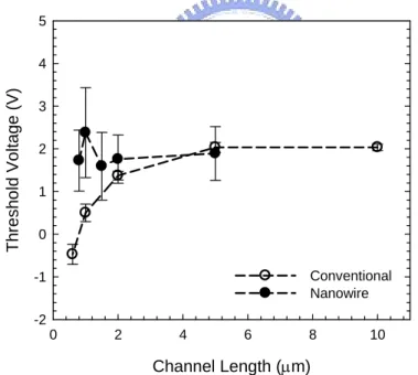
(19) Figure Captions. Chapter 2: Fig. 2-1 Schematic structure of NWTFTs. ............................................................................... 11 Fig. 2-2 (a) Top view and (b) cross-sectional view of the NWTFT. ........................................12 Fig. 2-3 Key processing steps for fabricating NWTFTs...........................................................14 Fig. 2-4 The cross-sectional view of NWTFTs taken by transmission electron microscopy (TEM). The deposited gate and the channel layer thicknesses are 100nm and 100nm, respectively. ...............................................................................................15 Fig. 2-5 Cross-sectional view of NW consisted of 200nm thick gate and 100nm channel layer. ................................................................................................................................16 Fig. 2-6 Cross-sectional view of NW with 100nm thick gate and 50nm channel layer. ..........17 Fig. 2-7 Measured width and thickness of the NW as a function of the OE time. ...................18 Fig. 2-8 Subthreshold characteristics of an as-fabricated NWTFT. .........................................19 Fig. 2-9 Output characteristics of an as-fabricated NWTFT. ...................................................19 Fig. 2-10 Subthreshold characteristics of NWTFTs which received different post-metal treatment. ................................................................................................................21 Fig. 2-11 Subthreshold characteristics of NWTFTs which received longer treatment.............22 Fig. 2-12 Subthreshold characteristics of NWTFTs with different channel width...................24 Fig. 2-13 Output characteristics of NWTFTs with different channel width.............................24 Fig. 2-14 Subthreshold characteristics of NWTFTs with different channel length..................25 Fig. 2-15 Output characteristics of NWTFTs with different channel length............................26 Fig. 2-16 Threshold voltage (Vth) as a function of channel length for NWTFTs with and without plasma treatment. ......................................................................................27 Fig. 2-17 On-state current as a function of channel length for NWTFTs with and without plasma treatment.....................................................................................................27. xvii.
(20) Fig. 2-18 Threshold voltage as a function of channel length for reference and NW devices.. 28 Fig. 2-19 Drain current per unit width as a function of channel width for control and NW TFTs. ...................................................................................................................... 30 Fig. 2-20 Schematic drawings of the cross-section of (a) the triangle NW and (b) conventional planar structure along the width direction.............................................................. 30 Fig. 2-21 Drive current (normalized to the channel width) as a function of channel width for control and NW devices. ........................................................................................ 31 Fig. 2-22 Mobility and subthreshold slope as a function of channel width for control and NW devices.................................................................................................................... 31. Chapter 3: Fig. 3-1 Typical transfer characteristics (ID-VG) of (a) MOSFET and (b) TFT device............ 34 Fig. 3-2 Schematic band diagrams of TFTs under various gate biases.................................... 35 Fig. 3-3 Schematic band diagrams of TFTs under various drain biases. ................................. 36 Fig. 3-4 Demonstration of activation energy extraction: (a) measuring off-state drain current under various temperatures, (b) performing Arrhenious plot, and (c) calculating activation energy from the fitted slope in (b)......................................................... 38 Fig. 3-5 Drain current per unit width of NWTFTs and conventional TFTs. ............................ 40 Fig. 3-6 Dependence of off-state leakage current for NWTFTs with different gate width...... 41 Fig. 3-7 Off-state leakage current of NWTFTs versus gate width........................................... 41 Fig. 3-8 Top view of the gate-to-drain overlap region in the device structure where major leakage current conducts........................................................................................ 42 Fig. 3-9 (a) Off-state I-V characteristics of a NWTFT measured at different temperatures. (b) Activation energy of NWTFTs measured at VD = 0.5 or 5 V as a function of gate voltage.................................................................................................................... 43 Fig. 3-10 Off-state characteristics of NWTFTs with and without NH3 plasma treatment....... 45 Fig. 3-11 Off-state leakage current of NWTFTs with and without NH3 plasma treatment as a function of gate width. ........................................................................................... 45 Fig. 3-12 Activation energy of NWTFTs with and without NH3 plasma treatment as a function of gate voltage........................................................................................................ 46 xviii.
(21) Fig. 3-13 Off-state characteristics of the devices with and without RTA treatment.................48 Fig. 3-14 Off-state leakage current of NWTFTs with RTA treatment as a function of gate width. ......................................................................................................................49 Fig. 3-15 Schematics of the NWTFT with hard mask modification. .......................................50 Fig. 3-16 Cross-sectional TEM of the NW-TFT embedded with nitride hard mask. ...............50 Fig. 3-17 Off-state characteristics of the devices embedded with hard mask. .........................51 Fig. 3-18 Off-state characteristics of devices with Si1-XGeX channels. ....................................52 Fig. 3-19 Leakage current flows near the drain side of NW-TFT. ...........................................53 Fig. 3-20 OSCR of devices with different modification schemes. ...........................................54. Chapter 4: Fig. 4-1 Schematic illustration of (a) CHEI and (b) DAHC in hot-carrier generation.............58 Fig. 4-2 Schematic illustration and operating configurations of the HCTFT test structure. ....62 Fig. 4-3 (a) Subthreshold and (b) output characteristics of as-fabricated test transistors (TTs). ................................................................................................................................63 Fig. 4-4 (a) Subthreshold characteristics of the test transistors before and after the hot-carrier stressing at VG/VD of 10 V/20 V for 1000 sec. (b) Subthreshold characteristics which are measured under reversed S/D mode. .....................................................65 Fig. 4-5 Subthreshold characteristics of (a) S-MT, (b) C-MT, and (c) D-MT transistors in the same test structure characterized in Fig. 4-4 before and after the hot-carrier stressing at VG/VD of 10 V/20 V for 1000 sec........................................................67 Fig. 4-6 Subthreshold characteristics of (a) TT, (b) S-MT, (c) C-MT, and (d) D-MT transistors in a test structure with a SPC poly-Si channel before and after the hot-carrier stressing at VG/VD of 9 V/18 V for 1000 sec..........................................................68 Fig. 4-7 Subthreshold characteristics of (a) TT, (b) S-MT, (c) C-MT, and (d) D-MT transistors in a test structure with an as-deposited poly-Si channel before and after the hot-carrier stressing at VG/VD of 6 V/12 V for 1000 sec. .......................................69 Fig. 4-8 Subthreshold characteristics of (a) TT, (b) S-MT, (c) C-MT, and (d) D-MT transistors in a test structure with a SPC poly-Si channel before and after the hot-carrier stressing at VG/VD of 6.5 V/13 V for 1000 sec.......................................................70 xix.
(22) Fig. 4-9 Threshold voltage shift of test structures under various hot-carrier stress conditions with constant VG/VD ratio of 0.5............................................................................ 71 Fig. 4-10 Subthreshold swing degradation of test structures under various hot-carrier stress conditions with constant VG/VD ratio of 0.5. ......................................................... 72 Fig. 4-11 Threshold voltage shift of test structures under various hot-carrier stress conditions at a fixed VD of 13 V. ............................................................................................. 73 Fig. 4-12 Subthreshold swing degradation of test structures under various hot-carrier stress conditions at a fixed VD of 13 V............................................................................. 73 Fig. 4-13 Subthreshold characteristics of (a) TT, (b) S-MT, (c) C-MT, and (d) D-MT transistors in the test structure with a SPC poly-Si channel before and after the hot-carrier stressing at VG/VD of 13 V/13 V for 1000 sec. .................................... 74 Fig. 4-14 Evolution of subthreshold characteristics of (a) TT, (b) S-MT, (c) C-MT, and (d) D-MT in test structures with a SPC poly-Si channel during hot-carrier stressing under VG/VD=6.5V/13V. ........................................................................................ 75 Fig. 4-15 Evolution of threshold voltage shift of a test structure during hot-carrier stress under VG/VD=6.5V/13V. .................................................................................................. 76 Fig. 4-16 Evolution of subthreshold swing degradation of a test structure during hot-carrier stress under VG/VD=6.5V/13V. .............................................................................. 76 Fig. 4-17 Schematic illustration of the hot-carrier-degradation mechanisms under VG/VD=6.5V/13V. .................................................................................................. 77 Fig. 4-18 Evolution of subthreshold characteristics of (a) TT, (b) S-MT, (c) C-MT, and (d) D-MT in a test structure with a SPC poly-Si channel during hot-carrier stressing under VG/VD=13V/13V. ......................................................................................... 78 Fig. 4-19 Evolution of threshold voltage shift of a test structure during hot-carrier stress under VG/VD=13V/13V. ................................................................................................... 79 Fig. 4-20 Evolution of subthreshold swing degradation of a test structure during hot-carrier stress under VG/VD=13V/13V. ............................................................................... 79 Fig. 4-21 Schematic illustration of the degradation mechanisms under VG/VD=13V/13V. The band diagram is taken near the source. .................................................................. 80 Fig. 4-22 Subthreshold swing of testers (TT and D-MT) after different duration of NH3 plasma treatment. ................................................................................................... 81 Fig. 4-23 Effective density-of-states distributions of TTs after different durations of NH3 xx.
(23) plasma treatment.....................................................................................................82 Fig. 4-24 Subthreshold characteristics of D-MTs before and after hot-carrier stressing of VG/VD = 6.5V/13V for 1000 sec. Samples received a plasma treatment of (a) 1 hour and (b) 2 hours. ..............................................................................................83 Fig. 4-25 Subthreshold swing shift of testers as a function of NH3 plasma treatment time. The shift represents the difference of the SS measured before and after hot-carrier stressing. .................................................................................................................83. Chapter 5: Fig. 5-1 Schematic illustration of the measurement setup........................................................87 Fig. 5-2 Waveforms of the stress pulse applied to the gate. .....................................................87 Fig. 5-3 Subthreshold characteristics of TTs before and after AC stress for 1000 seconds with the frequency of (a) 100kHz and (b) 1MHz. ..........................................................88 Fig. 5-4 Subthreshold characteristics of D-MTs before and after AC stress for 1000 seconds with the frequency of (a) 100kHz and (b) 1MHz. ..................................................89 Fig. 5-5 Subthreshold characteristics of S-MTs before and after AC stress for 1000 seconds with the frequency of (a) 100kHz and (b) 1MHz. ..................................................89 Fig. 5-6 On-current degradation under AC stress with different frequencies. .........................90 Fig. 5-7 Threshold voltage shift under AC stress with different frequencies...........................90 Fig. 5-8 Mechanism of AC stress induced degradation............................................................91 Fig. 5-9 On-current degradation after 100,000 repetitions of AC stressing as a function of frequency. ...............................................................................................................92 Fig. 5-10 On-current degradation of the testers after hot-carrier stressing with various rising time. ........................................................................................................................93 Fig. 5-11 On-current degradation of the testers after hot-carrier stressing with various falling time. ........................................................................................................................94 Fig. 5-12 On-current degradation of the testers after hot-carrier stressing as a function of rising time. ..............................................................................................................95 Fig. 5-13 On-current degradation of the testers after hot-carrier stressing as a function of falling time..............................................................................................................95 xxi.
(24) Fig. 5-14 Subthreshold characteristics of TTs after hot-carrier stressing with different falling time......................................................................................................................... 96 Fig. 5-15 Subthreshold characteristics of D-MTs after hot-carrier stressing with different falling time. ............................................................................................................ 97 Fig. 5-16 Schematic illustration of the relative location between the hot-carrier-damaged region and the leakage generation site. .................................................................. 98 Fig. 5-17 Evolution of subthreshold characteristics of (a) TT, (b) S-MT, (c) C-MT, and (d) D-MT in the tester during hot-carrier stressing under VG_high/VD=13V/13V, freq. = 500 kHz, tr = tf = 100ns.......................................................................................... 99 Fig. 5-18 Evolution of the shift in threshold voltage for the same tester shown in Fig. 5-17. .............................................................................................................................. 100 Fig. 5-19 Evolutions of the subthreshold swing shift of the same tester shown in Fig. 5-17.100 Fig. 5-20 Evolutions of on-current degradation of the same tester shown in Fig. 5-17. ....... 101. Chapter 6: Fig. 6-1 Subthreshold characteristics of TT measured at different temperatures. ................. 107 Fig. 6-2 Plots of T ⋅ (d log G / dVG ) as a function of 1000/T. .............................................. 108 Fig. 6-3 Extracted surface band-bending as a function of gate voltage................................. 108 Fig. 6-4 Calculated density-of-states as a function of surface band-bending. ....................... 109 Fig. 6-5 One Gaussian and two exponential distributions used to represent the extracted DOS distribution. ...........................................................................................................110 Fig. 6-6 Subthreshold characteristics of (a) TT and (b) D-MT, before and after hot-carrier stressing under VG/VD = 6.5V/13V for 1000 sec. .................................................111 Fig. 6-7 Effective density-of-states distribution of TT before and after hot-carrier stressing under VG/VD = 6.5V/13V for 1000 sec. ................................................................112 Fig. 6-8 Effective density-of-states distribution of D-MT (a) before and (b) after hot-carrier stressing under VG/VD = 6.5V/13V for 1000 sec. .................................................113 Fig. 6-9 (a) Relationship between gate voltage and extracted surface energy and (b) mapping of the increased DOS on subthreshold characteristics, before and after hot-carrier stressing under VG/VD = 6.5V/13V for 1000 sec. .................................................114 xxii.
(25) Fig. 6-10 Simulated subthreshold characteristics of D-MT (a) before and (b) after hot-carrier stressing under VG/VD = 6.5V/13V for 1000 sec.................................................. 115 Fig. 6-11 Evolution of subthreshold characteristics of D-MT in (a) logarithmic and (b) linear scales during hot-carrier stressing under VG/VD=6.5V/13V................................. 116 Fig. 6-12 Increase in density-of-states distributions of D-MT during hot-carrier stressing... 116 Fig. 6-13 Subthreshold characteristics of (a) TT, (b) S-MT, (c) C-MT, and (d) D-MT transistors in the test structure before and after the hot-carrier stressing at VG/VD of 10 V/20 V for 1000 sec......................................................................................... 117 Fig. 6-14 Density-of-states distributions of the TT and three MTs before HC stressing. ...... 118 Fig. 6-15 Density-of-states distributions of (a) D-MT, (b) C-MT, and (c) S-MT before and after hot-carrier stressing at VG/VD of 10 V/20 V for 1000 sec............................ 119 Fig. 6-16 Schematics of (a) top- and (b) cross-sectional view of the tester with indication of the induced damaged. ...........................................................................................120 Fig. 6-17 Simulated subthreshold characteristics using data collected from MTs. ................120. Chapter 7: Fig. 7-1 (a) Top view of the layout, (b) the optical microscopy image and (c) the schematics of the poly-Si NWTFT enhanced by MILC..............................................................126. Hand-crafted, perverse champion. Fig. 7-2 Schematics of the proposed bio-sensor realized by the NWTFTs. ...........................127. xxiii.
(26)
(27) Sec. 1.1 An overview of poly-Si thin-film transistors: trends in the development. Chapter 1 1 Introduction. Polycrystalline silicon (Poly-Si) thin-film transistors (TFTs) have been extensively used in many applications, including active-matrix liquid-crystal displays (AMLCDs) [1.1]-[1.4], memory devices [1.5]-[1.9], image sensors [1.10], and thermal printer heads [1.11]. Because of their better grain crystallinity, compared with the amorphous counterparts, better device performance such as carrier mobility and drive current can be realized in poly-Si TFTs.. 1.1 An overview of poly-Si thin-film transistors: trends in the development Thin-film transistors have been put into commercial use in the past decades. Since it is impossible to deposite single crystalline silicon (c-Si) film on glass substrate by low-pressure chemical vapor deposition (LPCVD) or plasma-enhanced chemical vapor deposition (PECVD), amorphous silicon or polycrystalline silicon are used as the channel materials in TFTs. By replacing quartz substrate with low-cost glass, and migrating the channel material from amorphous to polycrystalline, TFTs can now meet the requirement in fabrication cost, process temperature, and device performance. Because of the lack in short range order, the electron field effect mobility (μn) of amorphous silicon material is usually lower than 1 cm2/V-s. On the contrary, the mobility of poly-Si material varies from tens to hundreds cm2/V-s, depending on the process condition and the treatment in material preparation.. 1.
(28) Chapter 1 Introduction. Nonetheless, both are much lower than that of c-Si (~600 cm2/V-s). Therefore, how to increase the mobility of poly-Si is one of the most important challenges.. 1.1.1 Efforts in mobility enhancement Since mobility of poly-Si is mainly determined by the crystallinity, many studies focus on the grain size and the grain quality in poly-Si material. Although poly-Si can be directly deposited by LPCVD over 540-620˚C, its mobility is limited to about 10 cm2/V-s due to grain size of 100~500nm [1.12]. Solid phase crystallization (SPC) technique, where amorphous films was first deposited and then crystallized into poly-Si, has been shown to improve mobility and enhance grain size [1.13]. Usually, the crystallization process is performed in furnaces at 600˚C for 20-24 hours. The resultant grain size can exceed 1 μm, and the mobility can reach several tens of cm2/V-s. One of the practical limitations of the SPC technique is the temperature of 600˚C, which is still higher for most glass substrates. Processes where poly-Si preparation is carried out in lower temperatures hence were developed. Excimer laser anneal (ELA) [1.14]-[1.16] represents one of the promising candidates for low-temperature poly-Si (LTPS) technologies. By radiating pulsed excimer lasers on amorphous Si films, localized region can be melted and transformed into poly-Si. Since only the localized region was heated, the substrate temperature can be kept to lower than 400˚C. After adjusting energy density and duration of the laser pulse, along with scanning patterns [1.17] and substrate temperature, a high mobility of 280cm2/V-s can be achieved [1.18]. Another candidate for LTPS is the metal-induced lateral crystallization (MILC). It uses metals like Ni [1.19] or Pd [1.20] as the catalyst to promote the transition of a-Si to poly-Si in a lower temperature.. 1.1.2 Efforts in off-state leakage reduction In addition to mobility, another prime concern for TFT applications is their high off-state. 2.
(29) Sec. 1.2 An introduction of silicon nanowires. leakage current. Off-state leakage is a critical factor since it increases standby power dissipation. Most of the leakage is originated from the electrical field between gate and drain [1.21], combined with the impact of the defects inside channel material. Since the gate/drain bias is required for circuit operation, all efforts in off-state leakage reduction are focused on the reduction of trap state density or the uses of structural modification to reduce the localize electric field between gate and drain. The role of the trap states is to determine carrier generation rate and lifetime of generated electron-hole pairs. To reduce the trap density, employment of hydrogen passivation is a common technique [1.22]. Another approach is to enlarge grain size and reduce the number of the grain boundary in poly-Si material, because most of defects are located inside the grain boundaries. Equipped with the knowledge that the off-state leakage is originated near drain, by controlling the location of grain boundaries and keeping them away from the drain junction, the off-state leakage can also be effectively reduced [1.23]. Lightly-doped drain (LDD) is the most popular approach of structural modifications for leakage reduction [1.24][1.25]. It can effectively reduce the high electric field when devices are operated at off-state [1.26]. One of its impacts to TFTs is the attenuation of on-state current due to the addition of series resistance. There are other approaches which are based on the concept of LDD, but trying not to attenuate the on-state current [1.27]. In addition to LDD, other approaches such as field-induced drain [1.28] or multi-fingered gate [1.29] were also proposed to reduce the off-state leakage.. 1.2 An introduction of silicon nanowires Minimization is always the most critical issue in silicon technology. To enhance the output current and increase the density of devices per unit area on a chip, the geometry of device have been continually scaled down for past decades [1.30]. Nowadays with the 3.
(30) Chapter 1 Introduction. technology node at 65nm, the semiconductor industry has entered into nanoscale era. As the device is shrunk to the nanoscale regime, where the geometry of devices is smaller than 100nm, mechanical and electrical properties of the material may be different from those in the bulk material. As a result, the realization of some new structures and materials is likely. In addition to conventional planar structure which has been broadly employed in MOSFETs, some other structures such as FinFET [1.31], single-electron transistors [1.32], and nanowire [1.33][1.34], were proposed. Nanowires can be used as a conduction wire [1.35], a resistor [1.36], or a field-effect transistor (FET) [1.37]. Owing to its unique feature of high-surface-to-volume ratio, nanowire exhibits great potential for some specific applications such as bio-sensors [1.38][1.39], memory devices [1.40], and switches [1.41]. There are two major approaches for nanowire preparation. One is the top-down approach, which requires advanced lithographic tools like deep UV steppers [1.48][1.49]. Another is the bottom-up approach, such as growth of the nanowire by catalyst-assisted growth or epitaxy [1.50]. The former approach is very straight-forward, but costly. In contrast, the latter approach is very flexible for experimental studies, but has concerns of metal contaminations. Although many methodologies and materials have been proposed and demonstrated for nanowire preparation, the top-down approach, which is compatible with current MOSFET technology and without issues of contamination, is still the first choice for commercial manufacturing. More detail about the methodologies will be introduced in Section 2.1.. 1.3 Reliability issues in poly-Si TFTs As poly-Si TFTs were employed in the commercial applications, long term stability in device characteristics during circuit operations becomes another important issue. To keep circuits function properly, performance and electrical characteristics of TFTs must be within. 4.
(31) Sec. 1.4 Motivation of this study. the design specification, even after long-term operations. As a result, reliability issues need to be taken into considerations. Most of the reliability issues come from the low-temperature process needed for poly-Si TFTs and the nature of materials used in poly-Si TFTs. For instance, the deposited gate oxide, unlike the high-quality thermal oxide in MOSFET, may induce high gate leakage current or gate oxide failure after long-term operations [1.42][1.43]. Another example is hot-carrier degradation and self-heating in poly-Si TFTs. The former may result in shift of device characteristics owing to the localized damage induced in some portions of channel [1.44][1.45]. The latter may be ascribed to poor thermal-conducting of glass substrate and large amount of heat generated from on-current [1.46][1.47].. 1.4 Motivation of this study As mentioned in the above sections, the top-down approach is the best choice when integrating such a new device into current MOSFET technology. Since the cost is a critical concern for the top-down method, it is desirable to develop a new method that can not only be compatible with ULSI processes, but also reduces cost of fabrication. To achieve these goals, expensive advanced lithography must be avoided and an alternative approach needs to be adopted. It is required that the nanowire can not only be produced, but also be positioned at specific locations (i.e., the channel region). It is also desirable that this approach must be integrated with MOSFETs in a seamless manner. In lines with this, a novel method to fabricate nanowire thin film transistors (NWTFTs) was proposed and demonstrated in this dissertation. While characterizing the proposed NWTFT, we found that the off-state leakage current of device is much larger than we originally expected. After further investigation of the leakage current, we found that the current is proportional to the gate-to-drain overlap region. To 5.
(32) Chapter 1 Introduction. uncover the mechanism, more experiments were performed and some approaches were proposed in order to reduce the effect of such anomalous leakage. Eventually, we successfully demonstrated some process and device modifications, and new material for leakage reduction. The results are in a good agreement with our understanding. Similar to the device minimization which led us to the study of NWTFTs, the need in hot-carrier analysis also led us to the development of new test structures. Owing to the nature of non-uniform distributions of damages across the channel, the call for a test structure which is capable of spatially resolving the damages along the channel of stressed transistor is urgent. Information gathered from such test structures will be very valuable since it will enable us to easily locate the damage sites, analyze the mechanisms, and find cures to alleviate impacts of hot-carrier degradation. Again, this tester needs to be fully compatible with the ULSI processes. It would be even better if no additional mask is needed for such a tester. The outcome is a test structure which is capable of measuring the spatial and temporal evolution of hot-carrier degradation. Because the damage is non-uniformly distributed along the channel, it is very difficult to extract and analyze the difference in effective density-of-states (DOS) distributions before and after hot-carrier degradation. Since the proposed tester is capable of observing a localized degradation, density-of-states extraction technique can be adopted to investigate the impact of hot-carrier degradation on defect density in certain part of the channel. We have extracted the effective density-of-states distributions in damaged regions and validated the result by conducting the subthreshold characteristics using the extracted DOS and the device simulator.. 1.5 Organization of the thesis In this thesis, seven chapters are organized to present the detail of the aforementioned works. An overview of poly-Si TFTs is described in Chapter 1, together with the introduction 6.
(33) Sec. 1.5 Organization of the thesis. of silicon nanowires and the reliability issue in TFTs. Motivation of this study and organization of this work (i.e., the current section) are also included in this chapter. In Chapter 2, the nanowire thin-film transistors (NWTFTs) are demonstrated. Several methodologies are introduced and compared, providing the backgrounds of nanowire formation. The fabrication of proposed NWTFT is then described, followed by the detail in poly-Si nanowire formation and the investigation of factors that affect size and shape of the nanowire. Afterwards, on-state characteristics of NWTFTs are examined and discussed in Section 2.3. The characteristics of both as-fabricated and plasma-treated samples are demonstrated. The effects of post-metal treatment and geometric parameters on NWTFTs are then discussed. Last in this chapter, the advantages of nanowire channel are demonstrated by comparing with the traditional planar structure. In Chapter 3, the unique off-state leakage mechanism of proposed NWTFT is investigated. In the beginning of this chapter, some background knowledge such as off-state leakages in TFT, proposed mechanisms, analysis methodologies, and proposed leakage reduction methods, are introduced. Afterwards, the leakage mechanism of proposed NWTFT is investigated in Section 3.2. The origin of anomalous leakage is examined, as well as the effect of post-metal treatment. In Section 3.3, several modifications are proposed and demonstrated in order to alleviate the unique leakage. Rapid thermal annealing (RTA), inserted nitride mask, and poly Si1-XGeX are investigated and compared. An indicator called OSCR is also proposed to evaluate the effect of these modifications on off-state leakage reduction. In Chapter 4, the aforementioned novel tester for hot-carrier investigation is introduced, by describing design specifications and operating principles of the tester. The tester, which is called HCTFT, is then evaluated under various hot-carrier stressing experiments. The. 7.
(34) Chapter 1 Introduction. capability of the tester in spatially resolving hot-carrier degradation is demonstrated, followed by the discussion on sensitivity and stress conditions. We also demonstrate the application in observing temporal evolution during hot-carrier degradation in this chapter. At the end of this chapter, effects of post-metal plasma treatment on hot-carrier degradation are investigated. In Chapter 5, the HCTFTs are adopted in analyses of hot-carrier degradation under AC operations. The effects of several parameters, such as frequency, rising and falling times, are investigated and discussed. At last, a complicated case where two different types of degradation simultaneously occur at different part of the channel, along with the analysis using temporal evolution, are demonstrated. The analyses related to effective density-of-states distributions are performed and discussed in Chapter 6. Procedures of extracting effective density-of-states distributions and setup of simulation are described in detail. Afterwards, effective density-of-states distributions of the localized damaged regions are extracted. The information revealed by the analysis is then discussed. The extracted density-of-states distributions for both unstressed and stressed film are used to conduct simulations for subthreshold characteristics of TFTs and compared with the experimental data. Finally, the summaries and conclusions as well as some suggestions for future study are given in Chapter 7. References for each chapter are organized and listed at the end of this dissertation.. 8.
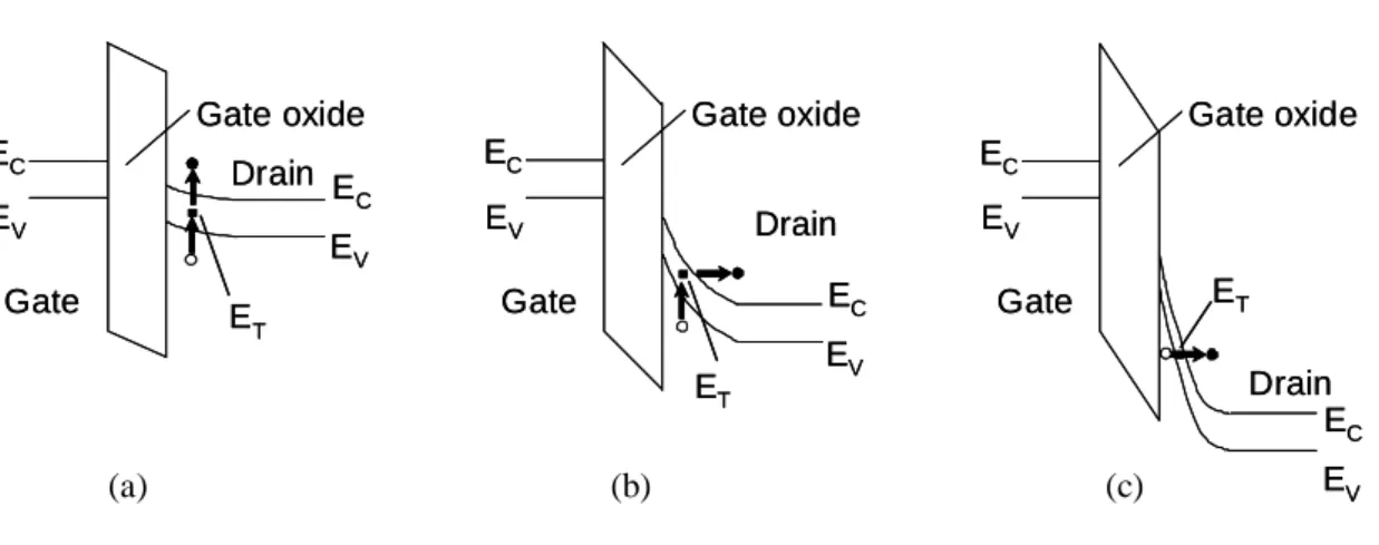
(35) Sec. 2.1 Background. Chapter 2 2 Nanowire TFTs with Self-Aligned Poly-Si Channels. 2.1 Background Minimization of silicon devices is being actively pursued. In this regard, Si nanowires (NWs) possess great potential for testing and understanding the fundamental role of dimensionality and size in device electrical properties. Owing to its inherent high surface-to-volume ratio, NWs can effectively suppress the short-channel effects normally encountered in nano-scale MOSFETs [2.1] and provide high surface sensitivity for sensing devices. Many potential applications of Si NWs have been investigated, including nano CMOS [2.1], novel logic devices [2.2], memory devices [2.3], NW TFTs [2.4], biosensors [2.5][2.6] , and nano-electromechanical switch devices [2.7]. Si NWs could be prepared by either top-down or bottom-up methods. The former approach uses advanced lithographic tools like deep UV steppers [2.1][2.3] and e-beam writers [2.6], to define the pattern of NWs. Silicon-on-insulator (SOI) wafers are usually required as the substrate to fabricate single-crystalline silicon (c-Si) NWs. Although well developed and mature for mass production purpose, top-down approach is very costly as it requires expensive equipments and cutting-edge technologies. The size of NWs is also restricted by the resolution limit of lithography and etching. To further shrink the width of the line into nano-scale regime, several techniques have been proposed to replace direct pattern-and-etching. One of the techniques is to use the spacer as the hard mask for etching. 9.
(36) Chapter 2 Nanowire TFTs with Self-Aligned Poly-Si Channels. [2.8]. This is because the formation of sidewall spacer is well developed, and the size of spacer can be carefully controlled to within several hundreds angstrom. By applying spacers as the hard mask, the Si layer under the spacer can be etched to form the NWs. Another technique is by shrinking the width of patterned oxide layer via over-time wet etching [2.9]. After the chemical shrink is complete and the width of under-cutted oxide is within the nano-scale, photo resist is then removed and shrunk oxide is used as the hard mask for etching of the underlying Si layer. Unlike the top-down approach, the bottom-up approach is very flexible for experimental studies. Instead of an existing Si layer on the wafer, NWs are prepared by catalyst-assisted growth or epitaxy. Several techniques are developed for this approach, such as vapor-liquid-solid (VLS) [2.10], solid-liquid-solid (SLS) [2.11], solid phase diffusion [2.12], molecular beam epitaxy (MBE) [2.13], oxide-assisted nucleation [2.14], and metal-organic chemical vapor deposition (MOCVD) [2.15]. Since the catalyst is usually metallic, contamination is a great concern. In addition, the positioning of NWs [2.16], and the control of structural parameters such as NW’s diameter, length, and orientation [2.17], could eventually hinder its use in practical manufacturing. A novel method for preparing nanowire TFTs (NWTFTs) is introduced and demonstrated in this chapter. The proposed method is simple and compatible with modern semiconductor processings. Moreover, it does not require costly lithographic tools. Solid-phase crystallized (SPC) poly-Si and as-deposited poly-Si1-xGex by low-temperature chemical vapor deposition (LPCVD) are used as the channel material. Performance comparisons with conventional planar devices, effects of plasma treatment, and geometric parameters are explored and addressed in this chapter. The conduction mechanism of the off-state leakage current and the methods for its reduction will be investigated and demonstrated in the next chapter.. 10. YOUNG OLE I LIVE.
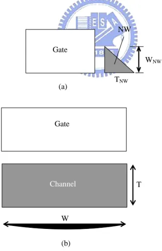
(37) Sec. 2.2 Fabrication of nanowire TFTs. 2.2 Fabrication of nanowire TFTs 2.2.1 Device Structure Figure 2-1 shows schematic structure of the proposed NWTFT. It adopts a side-gated scheme where two NW channels are formed on the sidewall of the gate. Source and drain (S/D) regions lying across the gate are defined simultaneously with the formation of NW channels in a self-aligned manner that will be described later. Another unique feature of the new structure is that a large portion of the NWs is inherently exposed to the environment which serves seamlessly as the sensing site when the device is used as a sensor. For example, for biologic sensor applications, the exposing NW surface serves as the sensing site and, after certain immobilization treatment, specific receptor agents are formed on the surface which could selectively detect the target species contained in the test solution [2.5], [2.6]. The top and cross-sectional views of the NWTFT are shown in Fig. 2-2(a) and Fig. 2-2(b), respectively. The definitions of dimensional parameters are also labeled in Fig. 2-2. It should be noted that “Gate Width” is different from “NW width”.. Source. Drain. Fig. 2-1 Schematic structure of NWTFTs.. 11.
(38) Chapter 2 Nanowire TFTs with Self-Aligned Poly-Si Channels. (a) Gate. Source Channel length Channel Drain. Gate Width (b) CVD oxide. NW thickness. Poly-Si. NW width. (Gate) thermal oxide Si substrate. Fig. 2-2 (a) Top view and (b) cross-sectional view of the NWTFT.. 2.2.2 Process of fabrication The key process for fabricating NWTFTs is briefly illustrated in Fig. 2-3. An n+ poly-Si gate of 100nm thick was first formed on a Si substrate capped with an oxide layer (Fig. 2-3(a)), followed by the deposition of oxide layer using low-temperature chemical vapor deposition (LPCVD). The oxide layer is 30nm thick, and serves as the gate dielectric. An amorphous Si layer of 100nm thick was then deposited by CVD, followed by an annealing step at 600 oC in N2 ambient for 24 hours to transform the amorphous Si into poly-Si (Fig. 2-3(b)). Subsequently, source/drain (S/D) implant was performed (Fig. 2-3(c)). It should be 12.
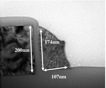
(39) Sec. 2.2 Fabrication of nanowire TFTs. noted that the implant energy was kept low so that most implanted dopants were located near the top surface of the Si layer. S/D photoresist patterns were then formed on the substrate by a standard lithography step. A reactive plasma etch step was subsequently used to etch the poly-Si layer. The sidewall Si channels were formed after this step in a self-aligned manner (Fig. 2-3(d)). Since the implanted energy is low, dopants in places other than S/D regions were removed during the etch step owing to the shallow project range. The S/D dopants were then activated by an annealing treatment. The fabrication was completed after the formation of test pads using standard metallization steps. To investigate the effectiveness of plasma passivation, some samples were treated in NH3 plasma at 300 oC after the metallization steps. To illustrate the impacts of using the NW channels on device performance, control devices with conventional top-gate and self-aligned S/D structure were also fabricated. These control devices have a 50 nm-thick SPC channel treated with the same SPC conditions as the NW split, and also received a plasma treatment in NH3 plasma at 300 oC for 1 hour.. 2.2.3 Formation of poly-Si nanowires The pictures taken by transmission electron microscopy (TEM) after channel formation are shown in Fig. 2-4. In Fig. 2-4(a), it can be clearly seen that the location of the NW channel is on the sidewall of the gate. The width and thickness of the NW can be characterized in Fig. 2-4(b), which are 21 and 23nm, respectively. Since the device adopts side-gate scheme, the width of the NW represents the width of the conduction channel. The size and shape of the spacer-like NW are determined by the following process parameters: thickness of the poly-Si gate, thickness of the deposited channel layer, time of etch, and recipe of the etcher (RIE). All four must be adjusted properly to obtain the desirable size of NW. The cross-sectional TEM view of the NW consisted of 200nm thick gate and 100nm thick channel layer is shown in Fig. 2-5. The etching recipe in this case is mainly 13.
(40) Chapter 2 Nanowire TFTs with Self-Aligned Poly-Si Channels. (a). (b). (c) ions. Dopant atoms. (d). Fig. 2-3 Key processing steps for fabricating NWTFTs.. 14.
(41) Sec. 2.2 Fabrication of nanowire TFTs. constructed by a break-through etch, a main etch (ME) with end-point detection, and an over etch (OE) of 60 seconds.The detail of the recipe is listed in Table 2-I. The resultant width and thickness of the NW are 174nm and 107nm, respectively. Although the shape in this case is rounded, the size of nanowire is still too large to meet the requirement (width < 100nm).. (a). (b). Fig. 2-4 The cross-sectional view of NWTFTs taken by transmission electron microscopy (TEM). The deposited gate and the channel layer thicknesses are 100nm and 100nm, respectively.. 15.
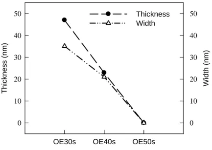
(42) Chapter 2 Nanowire TFTs with Self-Aligned Poly-Si Channels. 174nm 200nm. 107nm. Fig. 2-5 Cross-sectional view of NW consisted of 200nm thick gate and 100nm channel layer.. Etching step. Pressure (mTorr). RF Top power (W). RF Bottom power (W). Gas flow (sccm). Time (sec). Break-through. 5. 250. 200. Cl2: 80. 4. Main etch (ME). 17. 160. 33. Cl2: 22 O2: 1.5 HBr: 165. End-point detection. Over etch (OE). 25. 250. 33. O2: 2 HBr: 150. Table 2-I Details of the etching recipe during NW formation.. Samples with 100nm thick gate and 50nm thick channel layer are also fabricated. Owing to etching rate, the etching recipe is mainly constructed by a break-through etch and an over etch of 25 seconds. The resultant NW is shown in Fig. 2-6. The width and thickness of the NW in this case are 35nm and 34nm, respectively.. 16.
(43) Sec. 2.3 On-state Characteristics of nanowire TFTs. Fig. 2-6 Cross-sectional view of NW with 100nm thick gate and 50nm channel layer.. Since the time of main etch is controlled by end-point detection, over-etch time is used for NW size control. Several over-etch time are tested to determine the relationship between the over-etch time and the NW size. Samples with 100nm thick gate and 100nm thick channel layer are used in this experiment. The measured width and thickness of NW as a function of the OE time is illustrated in Fig. 2-7. Both NW thickness and width decrease with OE time. The results indicate that structural parameters of NW devices could be controlled reasonably. In other words, by carefully controlling the thickness of deposited film and the over-etch time, the structure can be easily shrunk into nano-scale regime.. 2.3 On-state Characteristics of nanowire TFTs Electrical characteristics of the fabricated nanowire TFTs are mainly characterized by the automated measurement setup constructed by an AglientTM 4156A semiconductor parameter analyzer and Interactive Characterization Software (ICS) software.. 17.
(44) Chapter 2 Nanowire TFTs with Self-Aligned Poly-Si Channels. Thickness Width. 50. 40. 40. 30. 30. 20. 20. 10. 10. 0. 0 OE30s. OE40s. Width (nm). Thickness (nm). 50. OE50s. Fig. 2-7 Measured width and thickness of the NW as a function of the OE time.. 2.3.1 Characteristics of as-fabricated nanowire TFTs “As-fabricated” devices mean that the devices received no post-metal treatment such as NH3-plasma or H2/N2 mixed anneal. Subthreshold and output characteristics of a typical poly-Si NW TFT device are shown in Fig. 2-8 and Fig. 2-9, respectively. In this example, the height of n+ poly-Si electrode is 100 nm, while the thickness of deposited Si layer and gate oxide are 100 and 30 nm, respectively. As can be seen in Fig. 2-8 and Fig. 2-9, good device performance with high on/off current ratio (around 105) and reasonable subthreshold swing (around 400 mV/decade) are achieved, even though the channel material quality and device structure are not optimized. The leakage current is rather high, presumably related to the process-induced damage during plasma etching and the gate-induced-drain-leakage (GIDL) occurred at the gate-to-drain overlap region. The mechanism and reduction of the leakage current will be discussed in Chapter 3.. 18.
(45) Sec. 2.3 On-state Characteristics of nanowire TFTs. 10-5 10. VD = 0.5V / 3V, W / L = 21 nm / 2μm. -6. Drain Current (A). 10-7 10-8 10-9 10-10 10-11 10-12 10-13 -2. 0. 2. 4. 6. 8. 10. Gate Voltage (V). Fig. 2-8 Subthreshold characteristics of an as-fabricated NWTFT.. 8.0 W / L = 21 nm / 2μm. Drain Current (μA). VG = 11V 6.0 VG = 10V 4.0 VG = 9V VG = 8V. 2.0. VG = 7V 0.0 0. 2. 4. 6. 8. 10. Drain Voltage (V). Fig. 2-9 Output characteristics of an as-fabricated NWTFT.. 2.3.2 Effects of post-metal treatment Post-metal hydrogenation has been reported to effectively reduce both the deep and tail states [2.18], and consequently enhance the performance of TFTs. Owing to the abundant grain boundaries and defects in TFTs, the effect of post-metal treatment in TFTs is more 19.
(46) Chapter 2 Nanowire TFTs with Self-Aligned Poly-Si Channels. important than that in MOSFETs. In recent years, plasma treatments in hydrogen ambient and other ambient such as deuterium [2.19], N2/H2 [2.20], or NH3 [2.21] have been investigated. The diffused hydrogen and nitrogen species have been reported to effectively passivate the dangling bonds, traps, and defects at grain boundaries and oxide/channel interface [2.22]. As a result, the device performance of TFTs improves, including better subthreshold characteristics, higher on/off current ratio, and lower barrier potential in the grain boundaries. To investigate the effect of post-metal treatment, the aforementioned “as-fabricated” devices were put under different ambients. In this work, both forming gas annealing (denoted as FG) in furnace and NH3 plasma treatment in PECVD were employed. For those which were annealed in forming gas, the devices were exposed in N2/H2 ambient at 400ºC for 30 minutes. For those which received plasma treatments, the devices were put in NH3 ambient at 300ºC, and exposed under a RF plasma of 200 watt for either 1 or 2 hours. Transfer characteristics of the samples which received different post-metal treatment are shown in Fig. 2-10. The width of NWs characterized in this experiment is 35nm. It can be clearly seen that the samples which received forming gas annealing exhibit only slightly better subthreshold swing, larger on-state current, and lower off-state leakage. Compared with FG annealing, dramatic improvement in device performance in terms of drastically reduced threshold voltage, steeper subthreshold slope, higher on-state current, and reduced leakage, is achieved with the plasma treatment. This is because the plasma can generate more excited hydrogen species, and provide more energy needed in diffusion and passivation. More defects will therefore be passivated, resulting in device performance improvement. The major performance parameters for the aforementioned NWTFTs are listed in Table 2-II . On and off current used to calculate on/off current ratio are defined as the current at VG=10V, VD=0.5V and VG= -3V, VD=0.5V, respectively.. 20.
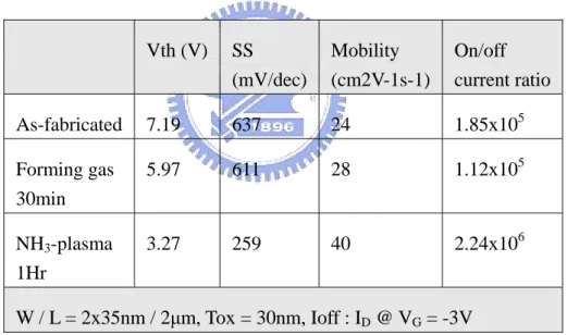
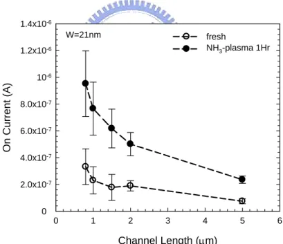
(47) Sec. 2.3 On-state Characteristics of nanowire TFTs. 10-5. VD = 0.5V / 3V, W / L = 35 nm / 2μm. 10-6 Drain Current (A). 10-7 10-8 10-9 10-10 10-11 as-fabricated FG 30min NH3-plasma 1Hr. 10-12 10-13 -2. 0. 2. 4. 6. 8. 10. Gate Voltage (V). Fig. 2-10 Subthreshold characteristics of NWTFTs which received different post-metal treatment.. Vth (V). SS (mV/dec). Mobility (cm2V-1s-1). On/off current ratio. As-fabricated. 7.19. 637. 24. 1.85x10⁵. Forming gas 30min. 5.97. 611. 28. 1.12x10⁵. NH3-plasma 1Hr. 3.27. 259. 40. 2.24x10⁶. W / L = 2x35nm / 2μm, Tox = 30nm, Ioff : ID @ VG = -3V Table 2-II Major performance parameters for NWTFTs which received different post-metal treatments.. Samples which received longer NH3 plasma treatments were also investigated. Transfer characteristics of NWTFTs which received different duration of NH3 plasma treatment are shown in Fig. 2-11. It can be seen that samples which received longer (e.g., 2-hours) treatment exhibit larger improvement on off-state leakage. The major performance parameters for the aforementioned NWTFTs are listed in Table 2-III. 21.
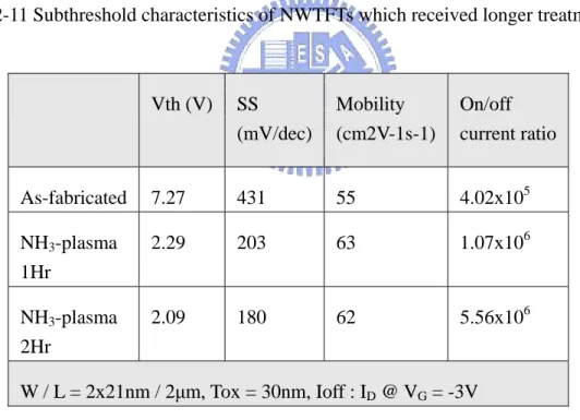
(48) Chapter 2 Nanowire TFTs with Self-Aligned Poly-Si Channels. 10-5. VD = 0.5V / 3V, W / L = 21 nm / 2μm. 10-6 Drain Current (A). 10-7 10-8 10-9 10-10 10-11 as-fabricated NH3-plasma 1Hr. 10-12. NH3-plasma 2Hr. 10-13 -2. 0. 2. 4. 6. 8. 10. Gate Voltage (V). Fig. 2-11 Subthreshold characteristics of NWTFTs which received longer treatment.. Vth (V). SS (mV/dec). Mobility (cm2V-1s-1). On/off current ratio. As-fabricated. 7.27. 431. 55. 4.02x10⁵. NH3-plasma 1Hr. 2.29. 203. 63. 1.07x10⁶. NH3-plasma 2Hr. 2.09. 180. 62. 5.56x10⁶. W / L = 2x21nm / 2μm, Tox = 30nm, Ioff : ID @ VG = -3V Table 2-III Major performance parameters for NWTFTs which received different duration of plasma treatment.. 2.3.3 Effects of geometric parameters of the nanowire channel As mentioned before, the size of nanowire channel can be controlled by over-etch time.. 22.
(49) Sec. 2.3 On-state Characteristics of nanowire TFTs. Unlike the conventional planar self-aligned counterpart where channel width only affects on-current, the size of the nanowire will influence electric characteristics in many aspects. This is owing to the edge effect of nanowire channel. In this section, impacts of geometric parameters of nanowire channel on electrical characteristics will be investigated. The transfer (subthreshold) and output characteristics of the NWTFTs with different channel width are shown in Fig. 2-12 and Fig. 2-13, respectively. In Fig. 2-12, it can be clearly seen that the NWTFT with W=21nm shows better electrical characteristics, including steeper subthreshold slope, higher on-state current, and lower off-state leakage current, compared with NWTFT with W=35nm. This could be ascribed to the better gate controllability and the fringing electrical field contributed by the edge of nanowire channel. The detailed explanation of the edge effect and the comparison between nanowire and conventional planar structure will be discussed in the next section. As shown in Fig. 2-13, it is interesting to note that the NWTFT with W=21nm possesses higher output current than the NWTFT with W=35nm. The threshold voltage difference owing to the steeper subthreshold slope may be the major cause. Since the NWTFT with W=21nm possesses lower threshold voltage, its output current will be larger from the well-known fundamental equation, in which the drain current can be expressed as:. I D = μ n COX. W (VG − VTH ) 2 L. Eq. 2-1. The extracted data in Table 2-II and Table 2-III also indicate that the mobility of the sample with W=21nm is higher than the sample with of W=35nm. This also contributes to the output-current enhancement.. 23.
(50) Chapter 2 Nanowire TFTs with Self-Aligned Poly-Si Channels. 10-5. VD = 0.5V / 3V, L = 2μm. 10-6. W = 35nm W = 21nm. Drain Current (A). 10-7 10-8 10-9 10-10 10-11 10-12 10-13 -2. 0. 2. 4. 6. 8. 10. Gate Voltage (V). Fig. 2-12 Subthreshold characteristics of NWTFTs with different channel width.. 14.0 W = 35nm W = 21nm. 12.0. L = 1.5μm. Drain Current (μA). VG = 7, 8, 9, 10, 11V 10.0 8.0 6.0 4.0 2.0 0.0 0. 2. 4. 6. 8. 10. Drain Voltage (V). Fig. 2-13 Output characteristics of NWTFTs with different channel width.. The effect of channel length is also investigated. In our experiments, NWTFTs with channel length ranging from 0.8μm to 5μm are used to study long and short channel effects, respectively. Figure 2-14 depicts subthreshold characteristics of NWTFTs with two extremes. 24.
數據

+7
相關文件
To reduce the leakage current related higher power consumption in highly integrated circuit and overcome the physical thickness limitation of silicon dioxide, the conventional SiO
To reduce the leakage current related higher power consumption in highly integrated circuit and overcome the physical thickness limitation of silicon dioxide, the conventional SiO 2
―Low-Temperature Polycrystalline Silicon Thin Film Transistor Nonvolatile Memory Using Ni Nanocrystals as Charge-Trapping Centers Fabricated by Hydrogen Plasma
a substance, such as silicon or germanium, with electrical conductivity intermediate between that of an insulator and a
• 後段工程是從由矽晶圓切割成一個一個的晶片 入手,進行裝片、固定、接合連接、注模成 形、引出接腳、按印檢查等工序,完成作為元
在1980年代,非晶矽是唯一商業化的薄膜型太 陽能電池材料。非晶矽的優點在於對於可見光
雙極性接面電晶體(bipolar junction transistor, BJT) 場效電晶體(field effect transistor, FET).
• 雙極性電晶體 (bipolar junction transistor , BJ T) 依結構區分,有 npn 型及 pnp 型兩種. Base
