國立臺灣大學工學院材料科學與工程學研究所 博士論文
Department of Materials Science and Engineering College of Engineering
National Taiwan University Doctoral Dissertation
原子層沉積之金屬氧化物及高分子/金屬氧化物超晶格 複合材料熱電性質及氣體滲透率研究
Thermoelectricity and gas permeability of metal oxide and metal oxide/polymer superlattice composites by atomic
layer deposition 施柏瑋 Bo-Wei Shih
指導教授: 蔡豐羽 博士 Advisor: Feng-Yu Tsai, Ph.D.
中華民國 108 年 12 月
December, 2019
誌謝
經過漫長的求學生涯,終於要卸下學生的角色了。在這最後一段的博士班歲 月中,可說是充滿磨練與挫折,但因有了許多人的鼓勵與幫助,讓我可以克服難 關,順利的走完這讓我成長最多的一個階段。
首先要感謝的是我的指導教授蔡豐羽博士所給予訓練。在研究過程中,教授 的信任讓我可以自由地發揮想像以及嘗試各種實驗;但在重要的時刻,您的及時 督導及糾正讓我可以發現自己的錯誤並修正。因此,在博士班的學習中,讓我培 養出可以獨立思考並謹慎自我審視的能力。於此同時,也要感謝 謝文斌教授長 期提供實驗資源讓我能順利完成研究,以及 郭錦龍教授於口試前及時雨的鼓勵 讓我混亂的思緒得以沉澱。
感謝實驗室學長姐們的知識分享和經驗傳授,讓我於研究初期可以快速的步 入軌道;也感謝各個學弟學妹們,你們的好學讓我在扮演學長這個角色時,可以 重新審視我所學的知識及技能。謝謝各位在實驗室遇到的人,你們豐富了我的研 究生活。接下來要感謝的是,系辦各位阿姨、牙醫系 琬瑜學姐和勝豪學長,以 及大學和高中的好友們,你們讓我在研究之餘或是研究疲憊時,可以向你們吐苦 水或是聽你們的幹話吐槽和各種八卦來調劑身心,謝謝各為讓我的台北生活更加 精采。
最後要感謝的是,一直以來支持我的媽媽、大姐一家、二姐一家、三姐以及 子華,你們不管是無形或是實值的照顧和關愛,是讓我有能力面對各項挑戰以及 獲得博士學位最重要的動力來源,謝謝你們無條件的陪伴,你們是我最重要的寶 藏。
摘要
本研究將探討由原子層沉積技術所製備之超晶格薄膜材料於熱電領域以及各 種不同領域之應用,如:可撓式超高阻氣性薄膜以及奈米孔洞材料之開發。隨著 穿戴型電子裝置的普及以及積體電路尺度的微縮,如何回收裝置操作時所產生的 廢熱和冷卻裝置中各種微型晶片以達到再生能源之利用和裝置元件壽命的延長為 現今科學家及工業界爭相研究之項目。其中薄膜熱電技術為一可同時解決這些問 題之技術,但其實用性仍受限於高效能薄膜熱電材料以及高可靠性熱電薄膜製程 技術之缺乏。在材料選擇方面,相較於傳統的重金屬化合物塊材熱電材料,金屬 氧化物半導體薄膜熱電材料具備多項優勢,包括價格低廉、化學性質穩定、環境 友善、且薄膜製備簡易等,因此為極受看好之新世代熱電材料。然而,金屬氧化 物雖具有良好的電導率及 Seebeck coefficient,但其熱導率亦極高,使其代表 熱電效能之 ZT 值難以提高。本研究將利用具高可靠性之薄膜沉積技術─原子層 沉積技術(ALD)製備技術純熟之氧化鋅薄膜並藉由進行新穎觀念之研究,以大幅 提升之氧化鋅薄膜之熱電效能,此外,亦進行將超晶格薄膜應用於可撓式超高阻 氣性薄膜以及奈米孔洞材料之開發的研究。本論文主要的研究項目有下列五點:
(1) 在 ALD 氧化鋅中,引入不同之摻雜物以形成週期性超晶格結構,並探討
摻雜物種類、濃度、分布方式以及超晶格週期對於熱電效應之影響。在 我們的研究中顯示,高原子量以及離子半徑匹配於基質之摻雜物在同時 使用傳統摻雜技術和本實驗室所開發的混合層摻雜技術下,可對基質之 熱電效能有最佳之提升,其幅度可達 12 倍。
(2) 在 ALD 反應中,使用具18O 與16O 同位素之前驅物以形成具有同位素之超
晶格薄膜,此研究就可在維持前項研究中所最佳化之電性條件下,更進 一步的降低熱導率。於結果中顯示,50%的同位素混摻並在疊層週期約為 10 奈米時,可將前項研究中最佳之熱導率再下降 20~25%。
(3) 開發新穎分子層沉積(MLD)之有機高分子導電薄膜,與金屬氧化物層交替 沉積形成高分子/氧化物超晶格薄膜,藉由大量的有機/無機界面來大幅 降低材料熱導率,但仍維持高導電度。於導電高分子的研究上,我們成
功開發出兩款高分子薄膜,其中一款電導率可高達 500 S cm-1。而在高
分子/氧化物超晶格薄膜的熱電性質表現上,在最佳化的結構中,其熱電 效能可提升 7 倍。
(4) 開發具抗水解能力之高分子即其所形成之高分子/氧化物超晶格薄膜阻氣
性質研究。於結果中,該高分子即其所形成之超晶格薄膜皆於高濕度的 環境下,具有較高的穩定性。
(5) 開發低溫熱裂解技術,以製備奈米孔洞材料。於研究中發現,在水氣的
幫助下,可大幅降低 alucone 之熱裂解溫度以形成奈米孔洞材料。其最 佳化的條件中,可有效移除高達 70%的碳含量,且退火溫度可低於 100
℃。因此,此技術將使奈米孔洞材料可沉積於高分子基板以及應用於各 種軟性電子元件中。
關鍵詞:薄膜熱電材料、原子層沉積技術、分子層沉積技術、氧化鋅、超晶格薄 膜、高分子奈米複合材料、可撓式高阻氣性薄膜、奈米孔洞材料。
Abstract
Thermoelectric thin films are an important type of materials for the management and recycling of waste heat in the ever-shrinking electronic devices, but their
development has been hindered by the dearth of methods for fabricating high-quality thin films with adequate thermoelectric performance, i.e. high Seebeck coefficient, high electrical conductivity, and low thermal conductivity. This study develops high-quality superlattice thin films based on metal oxides and conducting polymers by atomic layer deposition (ALD) and molecular layer deposition (MLD), aiming to realize significant enhancement in the thermoelectric figure of merit, or ZT value, of the resultant thin films. Additionally, the gas permeation properties of the ALD/MLD superlattice thin films are also examined. Key results and findings of this work are summarized as follows.
(1) Effects of composition and structure on the thermoelectric properties of metal oxide superlattice thin films: We used ZnO as our host material, into which we insert HfO2, ZrO2, or TiO2 guest layers with various thicknesses and
periodicities as both electrical dopants and phonon-scattering centers. We arrived at the following conclusions: (i) of the 3 types of guest layers, HfO2
showed the best overall enhancement in ZT, by a factor of 12, over the ZnO host owing to Hf’s similar ionic radius to Zn’s and high atomic mass; (ii) the
optimal electrical performance was achieved by forming the guest layers as a mixture of both ZnO and the guest in a periodicity of 1 mixed monolayer per 24 ZnO monolayer; (iii) the best phonon-scattering effect was obtained by inserting 7 guest monolayers for every two periods of the structure described in (ii).
(2) Effects of incorporating O18 isotope into the metal oxide superlattice on its thermoelectric properties: Based on the optimal structure we developed in (1), we found that the ZT could be further increased by around 20% by replacing 50% of the oxygen content with O18 in a periodicity of 10 nm O16/10 nm O18. (3) Development of novel MLD conducting polymers and their superlattices with
metal oxide semiconductors: Two polymers, polyaniline and poly(3,4- ethyelenedioxythiophene) (PEDOT), were successfully deposited with electrical conductivity of up to 500 S cm-1. Superlattice films composed of alternating 4 periods of ALD mix 19:1 HZO and 6 cycles of MLD PEDOT were found to offer the maximum improvement in ZT, by ~700%, over that of the undoped ZnO.
(4) Development of hydrolysis-resistant MLD polymer films to fabricate ALD/MLD nanolaminated high-performance gas barrier films: Polyamide (Poly(imino-carbonyl-1,4-phenylene-carbonyl-iminoethylene)) films deposited
from terephthaloyl chloride and ethylenediamine were found to provide the best long-term stability under humid condition among several polyamide films studied.
Key words: Thin-film thermoelectrics, atomic layer deposition (ALD), molecular layer deposition (MLD), zinc oxide (ZnO), superlattice, conducting polymer nanocomposites, flexible gas barrier, nanoporous materials.
Table of Contents
誌謝 ... i
摘要 ... ii
Abstract ... iv
Table of Contents ... vii
List of Figures ... xii
List of Tables ... xix
Chapter 1 Introduction ... 1
1.1 Overview of thermoelectricity ... 1
1.2 Fundamental of thermoelectric effect ... 4
1.2.1 Origin of thermoelectric effect ... 4
1.2.2 Trade-off between electrical conductivity and Seebeck coefficient ... 8
1.2.3 Thermal conductivity of materials ... 11
1.2.4 The figure of merit, ZT ... 14
1.3 Thermoelectricity in thin films ... 16
1.3.1 Size effect ... 16
1.3.2 Superlattice(Nanolaminates) ... 17
1.3.3 Advantages of thin film thermoelectric materials ... 19
1.4 Fundamental of atomic layer deposition and its advantages of depositing thin film thermoelectric materials ... 22
1.4.1 Atomic layer deposition(ALD) ... 22
1.4.2 Molecular layer deposition(MLD) ... 24
1.4.3 Advantages of ALD on depositing thin film thermoelectric materials ... 26
1.5 Literature review of thin film thermoelectric materials deposited by ALD 29 1.6 Applications of ALD/MLD superlattices ... 32
1.6.1 Flexible high performance gas barrier ... 32
1.6.2 Nanoporous materials ... 34
1.7 Motivation and objective statements ... 36
1.8 Research approach ... 39
1.8.1 High valence and high atomic weight metal ion doping ... 39
1.8.2 Isotope superlattice ... 40
1.8.3 Novel MLD conducting polymer development and the metal oxide/polymer superlattice deposition ... 41
1.8.4 Anti-hydrolysis polymer development ... 43
1.9 Dissertation Organization ... 45
Chapter 2 Experimental methods ... 47
2.1 Equipment and experiment details ... 47
2.1.1 ALD and MLD deposition systems ... 47
2.1.2 Conventional and mixed ALD metal ion doping process ... 48
2.1.3 Oxygen isotope incorporated superlattice ... 51
2.1.4 MLD conducting polymer process ... 52
2.1.5 Anti-hydrolysis polymers and metalcone process ... 54
2.2 Thin film characteristics analysis ... 56
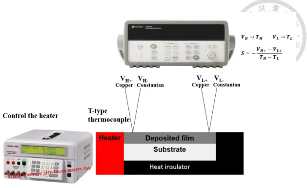
2.2.1 Measurements of electrical conductivity and Seebeck coefficient ... 56
2.2.2 Measurement of thermal conductivity by the time-domain thermoreflectance method (TDTR) ... 57
2.2.3 Quartz crystal microbalance (QCM) ... 61
2.2.4 Spectral characterization... 61
2.2.5 Transmission electron microscopy (TEM) ... 62
2.2.6 Micro-figure measurement (Alpha-step) ... 63
2.2.7 Gas barrier performance measurements ... 63
2.2.8 Thermogravimetric analysis (TGA) ... 64
Chapter 3 Metal oxide superlattice ... 65
3.1 Selection of dopants ... 65
3.2 Distribution Patterns of dopants ... 72
3.2.1 Conventional versus mixed ALD doping processes ... 72
3.2.2 Combination of conventional and mixed ALD doping processes ... 79
3.3 Isotope superlattice ... 92
3.3.1 Modification of deposition parameters ... 92
3.3.2 Influence on thermoelectric properties ... 94
3.4 Summary ... 100
Chapter 4 Metal oxide/polymer superlattice ... 102
4.1 Poly(3,4-ethylenedioxythiophene) (PEDOT) ... 102
4.1.1 The deposition of PEDOT ... 102
4.1.2 Interface-engineering of metal oxide/PEDOT superlattice ... 108
4.1.3 Superlattice deposition and thermoelectric performance ... 114
4.2 Polyaniline ... 127
4.3 Polythiophene ... 130
4.4 Summary ... 132
Chapter 5 Long-term stable gas barrier ... 134
5.1 The deposition of polyamide ... 134
5.2 The gas barrier performance of polyamide and HfO2/polyamide superlattice 143 5.3 The deposition of polyester ... 146
5.4 Summary ... 149
Chapter 6 Conclusions ... 150
Reference ... 153
Appendix Nanoporous materials ... 161
Other data ... 169
List of Figures
Chapter 1
Figure 1.1: Operating principle of TE materials. ... 3
Figure 1.2: Best ZT value for bulk n-type and p-type TE materials. ... 3
Figure 1.3: Illustration of model for deducing. ... 6
Figure 1.4: The Fermi Dirac distributions at each end and difference between them. ... 6
Figure 1.5: The dependence of Seebeck coefficient on DOS over energy states. ... 7
Figure 1.6: Fermi window and Fermi-Dirac distribution. ... 10
Figure 1.7: Tendency of Seebeck coefficient and electrical with regard to the location of Fermi window. ... 11
Figure 1.8: Contribution of 𝜅𝜅𝑒𝑒𝑒𝑒 and 𝜅𝜅𝑝𝑝ℎto 𝜅𝜅𝑡𝑡𝑡𝑡𝑡𝑡𝑡𝑡𝑒𝑒for different types of materials. ... 15
Figure 1.9: The optimization of ZT through carrier concentration tuning.. ... 15
Figure 1.10: The schematic diagram of the density of states for electrons in different dimension based on parabolic band structure. ... 21
Figure 1.11: The schematic diagram of energy filtering effect in superlattice. ... 21
Figure 1.12: The schematic illustration of ALD film growth mechanism. ... 27
Figure 1.13: ALD window, the dependence of growth rate per cycle on temperature. .. 28
Figure 1.14: The schematic illustration of MLD polyester film growth mechanism. .... 28
Figure 1.15: The structure of PA32. ... 33
Figure 1.16: The schematics of torturous path of inorganic-organic multilayer gas barrier. ... 33
Figure 1.17: The schematic illustration of the evolution of ALD/MLD superlattice after post-annealing in various atmosphere. ... 35
Figure 1.18: The tunability of pore size resulted from ALD/MLD superlattice. ... 35
Figure 1.19: The reaction mechanism of MLD PEDOT95. ... 43
Chapter 2
Figure 2.1: The scheme illustration of home-made system for measuring Seebeck coefficient. ... 57Figure 2.2: The multilayered structure used for simulation. ... 59
Figure 2.3: The result of ZnO thermal conductivity by TDTR method. ... 60
Figure 2.4: The schematic layout of TDTR apparatus. ... 60
Figure 2.5: The calculated 𝑆𝑆𝑆𝑆 for each parameters in simulation. ... 61
Chapter 3
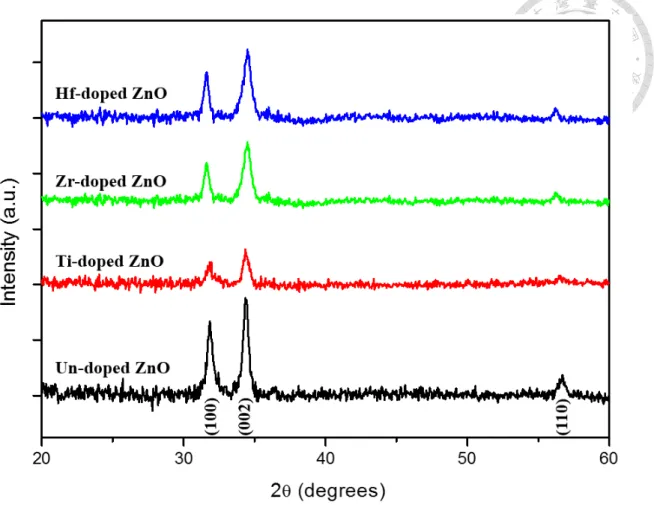
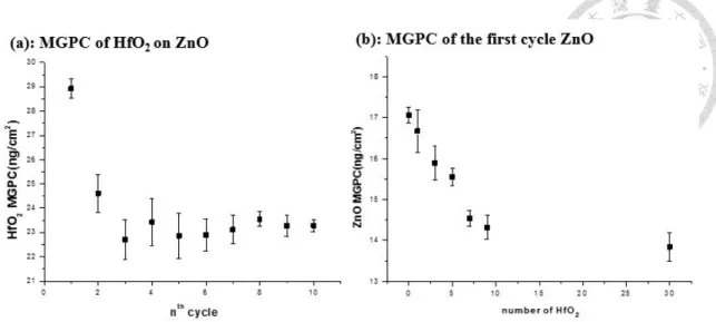
Figure 3.1: The XRD patterns of undoped ZnO and all con 9:1 doped ZnO. ... 71 Figure 3.2: The schematic illustration of depositing dopant layer by conventionalprocess and mixed ALD doping process. ... 78 Figure 3.3: XRD comparison for (a) same period length; (b) densely inserted mixed ALD doping; (c) same Hf content. ... 78 Figure 3.4: The ZnO films doped with a combination of conventional and mixed HfO2
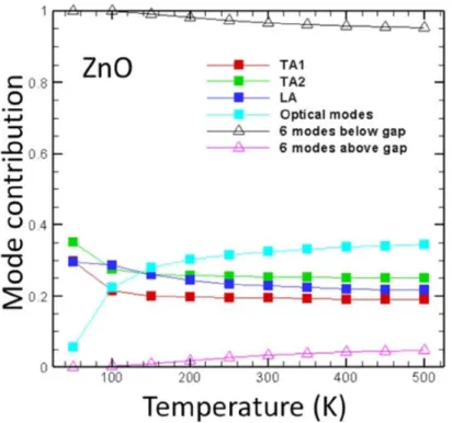
dopant layers. ... 88 Figure 3.5: The illustration and the nomenclature of structures with 1 period of mix 24:1 HZO and varied cycles of conventional HfO2 layer. ... 88 Figure 3.6: MGPC of (a) HfO2 on the surface of 24 cycles ZnO and (b) the first cycle ZnO on the various cycles of HfO2 acquired from in-QCM analysis. ... 89 Figure 3.7: Cross-sectional TEM images of the mix 24:1 HZO films inserted with (a) 3, (b) 5, (c) 7 cycles of the conventional dopant layer at each 1 period length (24 ZnO cycles/1 m-dopant cycle/24 ZnO cycles)... 89 Figure 3.8: The energy band alignment of ZnO and HfO2. ... 90 Figure 3.9: The transportation of carriers in mix 24 / nH (a) n<7; (b) n=7; (c) n>7. ... 90 Figure 3.10: Cumulative lattice thermal conductivity of bulk ZnO at 300 K simulated by Karttunen et al. 100. ... 91 Figure 3.11: The nomenclature of structures which are isotope incorporated... 98 Figure 3.12: The contribution ratio of each phonon modes in ZnO which is simulated by Wu et al.103. ... 98
Figure 3.13: The phonon group velocity as a function of frequency for ZnO simulated by Wu et al.103. ... 99 Figure 3.14: The simulation done by Wang et al.104 (a) phonon dispersion curves of wurtzite ZnO; (b) vibrational density of states of wurtzite ZnO. ... 99
Chapter 4
Figure 4.1: The photographs of deposited PEDOT films and blank glass substrates. .. 106 Figure 4.2: The FITR spectrum of deposited PEDOT films. ... 106 Figure 4.3: The UV-Vis spectrum of deposited PEDOT films. ... 107 Figure 4.4: The in-situ QCM results of the deposition of PEDOT on the surface of ZnO using two kinds of pulse sequences. ... 112 Figure 4.5: The cross sectional TEM images of deposited films in the structure of
6×(80-cycle ZnO/ 1-cyle PEDOT). ... 112 Figure 4.6: The mass gain of ZnO in steady-growth region and that on the surface of inserted PEDOT with various modifications. ... 113 Figure 4.7: The mass gain of H2O on surface covered by redundant SbCl5. ... 113 Figure 4.8: The XRD patterns of ZnO deposited by ALD and MLD systems. ... 124 Figure 4.9: The mean grain size calculation of mix 19:1 HZO by Scherrer equation. . 125 Figure 4.10: The cross-sectional TEM images of HZO/PEDOT superlattices with (a) 1-
cycle; (b) 6-cycle inserted PEDOT. ... 125 Figure 4.11: The schematic illustration of superlattice-structure and series-resistance model in our calculation. ... 125 Figure 4.12: The estimated interface thermal conductance in ZnO/hydroquinone/ZnO superlattice done by Ashutosh Giri et al. ... 126 Figure 4.13: The schematic illustration of energy band alignment of PEDOT and ZnO.
... 126 Figure 4.14: The photograph of 15 and 30nm polyaniline thin films on glass substrates.
... 129 Figure 4.15: The FTIR spectrum of ~30nm polyaniline. ... 129 Figure 4.16: The in-situ QCM results (a) deposition of polythiophene while pulsing thiophene twice; (b) pulse VOCl3 alone; (c) increasing N2 flow rate transiently. ... 131
Chapter 5
Figure 5.1: The QCM results by the usage of MC and piperazine in deposition of
polyamide at varied deposition temperature (a) 100°C; (b) 120°C. ... 139 Figure 5.2: The QCM results by the usage of MC and 1,8-diaminooctane in deposition of polyamide at varied deposition temperature (a) 120°C; (b) 100°C. ... 139 Figure 5.3: The QCM results of 100-cycle polyamide deposited by the usage of MC and
1,8-diaminooctane at 100°C. The inset is the zoom-in of the mass gain at latter cycles.
... 139
Figure 5.4: The FITR spectrum of polyamide deposited by the usage of MC and 1,8- diaminooctane. ... 140
Figure 5.5: The QCM result by the usage of terephthaloyl chloride and ED in deposition of polyamide at 120°C. ... 140
Figure 5.6: The QCM result of the multiple pulse of single precursor. ... 141
Figure 5.7: The QCM result of polyamide by the usage of terephthaloyl chloride and ED with re-nucleation layers. ... 141
Figure 5.8: The FITR spectrum of polyamide deposited by the usage of terephthaloyl chloride and ED. ... 142
Figure 5.9: The QCM results of varied pulse time of EG (a) 0.02 s; (b) 0.10 s. The insets are the mass gain at latter cycles. ... 147
Figure 5.10: The QCM result of polyester at 180°C with 0.02 s pulse of EG. ... 147
Figure 5.11: The schematic illustration of single and double reaction in MLD. ... 148
Figure 5.12: The reaction mechanism of the self-condensation of MC monomers. ... 148
Appendix
Figure A.1: The QCM result of alucone with varied exposure time (a) without; (b) 5 s;
(c) 15 s of EG deposited at 105 °C. ... 166 Figure A.2: The cross-sectional SEM images of alucone film with the exposure of EG.
... 166 Figure A.3: The TGA result of the SiO2 nanoparticles. ... 167 Figure A.4: The TGA results of the SiO2/alucone core-shell particles. ... 167 Figure A.5: The TGA results of the SiO2/alucone core-shell particles after varied low- temperature pyrolysis process. ... 168
List of Tables
Chapter 1
Table 1.1: The current progress in ALD ZnO thin film thermoelectric materials. ... 31
Chapter 2
Table 2.1: ALD parameters of depositing undoped ZnO. ... 49Table 2.2: ALD parameters of depositing conventional process metal ion doped ZnO. 49 Table 2.3: ALD parameters of depositing mixed ALD doping process metal ion doped ZnO. ... 50
Table 2.4: MLD parameters of depositing polythiophene. ... 53
Table 2.5: MLD parameters of depositing polyaniline. ... 53
Table 2.6: MLD parameters of depositing PEDOT. ... 53
Table 2.7 MLD parameters of depositing polyester. ... 55
Table 2.8: MLD parameters of depositing polyamides. ... 55
Table 2.9: MLD parameters of depositing alucone at 105°C. ... 55
Chapter 3
Table 3.1: The thermoelectric characteristic of undoped ZnO, Ti:ZnO, Zr:ZnO and Hf:ZnO... 69Table 3.2: The concentration of dopant measured by XPS and atomic number density of dopants. The number density is calculated by using composition ratio, film thickness and density41,99. ... 70 Table 3.3: Bond energy of metal/ligand and metal/oxygen and the difference between bond energies (ΔBE= BE metal/oxygen−BE metal/ligand). ... 70 Table 3.4: The thermoelectric characteristic of undoped ZnO, conventional process and mixed ALD doping process HZO. ... 76 Table 3.5: The concentration of dopant measured by XPS and atomic number density of Hf. The number density is calculated by using composition ratio, film thickness and density. ... 77 Table 3.6: The thermoelectric characteristic of the mix 24:1 HZO films inserted with 5- cycle conventional HfO2 layers at three periodicities (as illustrated in Figure 3.4). ... 86 Table 3.7: The thermoelectric characteristic of undoped ZnO and the films composed of 1 period of mix 24:1 HZO and varied cycles of conventional HfO2 layer.. ... 87 Table 3.8: The electrical characteristic, thickness and the refractive index of mix 24 / 7H-16O, mix 24 / 7H-18O and modified mix 24 / 7H-18O. ... 93 Table 3.9: The thermoelectric characteristic of undoped ZnO, mix 24 / 7H and 18O incorporated superlattice... 97
Chapter 4
Table 4.1: The characteristic of deposited PEDOT films. ... 106 Table 4.2: The electrical conductivity of PEDOT/HZO superlattice with various
modifications in the structure of 6×(4 periods mix 19:1 HZO + 1-cyle PEDOT) ... 112 Table 4.3: The electrical properties of ZnO and mixed HZO with varied insertion
periodicity of mixed doping layers. ... 123 Table 4.4: The thermoelectric characteristic of the HZO/PEDOT superlattice films with varied periodicities of mix 19:1 HZO host layers. ... 123 Table 4.5: The thermoelectric characteristic of the HZO/PEDOT superlattice films composed of alternating 4 periods of mix 19:1 HZO and varied cycles of PEDOT. ... 124 Table 4.6: The relevance of polyaniline growth rate on the temperature of SbCl5. ... 129
Chapter 5
Table 5.1: The structure of precursors, polymers and deposition temperatures in the deposition of polyamides. ... 138 Table 5.2: HeTR of varied samples before/after damp-test (85°C, 85%RH, 36 hours) and WVTR of superlattice-based gas barrier. The unit of HeTR and WVTR is cc day-1 m-2 and g day-1 m-2, respectively. ... 145
Chapter 1
Introduction
1.1 Overview of thermoelectricity
According to Quadrennial Technology Review 2015 from the United States Department of Energy, it is estimated that around 20~50% of industrial energy use becomes waste heat (e.g. hot exhaust gases, hot equipment surface and the heat pump away by cooling systems) and is then discharged into the environment1. Besides, household electrical appliances and personal portable devices also produce waste heat during operation. Recycling of such waste heat into useable energy will greatly reduce energy consumption and lessen the environmental impacts of industrial productions.
Thanks to its considerable advantages, such as scalability, reliability, zero extra energy input and no contamination, thermoelectric power generation is one of the best methods for recycling waste heat2. Thermoelectricity (TE) is a physical phenomenon where heat is converted into electrical energy directly, and vice versa. The TE effect was first discovered by Italian scientist Alessandro Volta, and then became widely known thanks to the work of Baltic German physicist Thomas Johann Seebeck3. A schematic illustration of the operating principle of the TE effect is shown in Figure 1.1. When a
chemical potential gradient of the charged carriers. The chemical potential gradient makes the charged carriers flow and then accumulate respectively at the hot and cold end of the TE material to form an electromotive force (EMF). The formed EMF can output electrical power if the ends of the TE material are attached to devices, thereby converting waste heat into useable electrical energy directly.
The efficiency of the thermoelectric effect of a material can be quantified by a figure of merit, ZT, which is defined as ZT =𝑆𝑆2𝜅𝜅𝜎𝜎𝑇𝑇, where S is the Seebeck coefficient, which is the ratio of the formed EMF over the applied temperature difference (−∆𝑉𝑉∆𝑇𝑇); σ the electrical conductivity of the material, κ the thermal conductivity, and T the absolute temperature.
As a high efficiency TE material, three properties are required. First, a high absolute value of Seebeck coefficient, which offers a high EMF to output electrical work, is required. Second, a high electrical conductivity ensures a low energy
dissipation as Joule heat during operation. Third, a low thermal conductivity is able to maintain not only high but also consistent temperature difference between the two ends of the material. In general, ZT>1 is the criterion to determine whether a TE material is practically usable or not. The summary of some common bulk n-type and p-type TE materials with high ZT values is shown in Figure 1.2.
Figure 1.1: Operating principle of TE materials.
Figure 1.2: Best ZT value for bulk n-type and p-type TE materials.
1.2 Fundamental of thermoelectric effect 1.2.1 Origin of thermoelectric effect
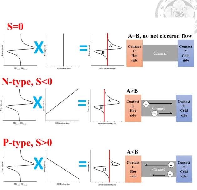
In this section, we use a qualitative way to deduce the origin of thermoelectric effect. First, a material with a finite thin thickness is divided into three parts, and each part is named as Contact1, Channel and Contact2, respectively. The schematic
illustrations of qualitative derivation are shown in Figure 1.3, Figure 1.4.and Figure 1.5.
When the temperature is homogeneous inside the entire material, the Fermi levels are the same at Contact1 and Contact2. However, when the thermal energy is applied to the material from a single side, a temperature gradient is created across the material. Here, we assume that Contact1 is the hot side and Contact2 is the cold side. A portion of electrons at the hot side gains sufficient kinetic energy and then is able to transit to the
higher energy states. In this transition process, the distribution of electrons over energy states at particular temperature is described by Fermi-Dirac distribution,𝑓𝑓(E) = 1
𝑒𝑒𝐸𝐸−𝜇𝜇𝑘𝑘𝐵𝐵𝑇𝑇+1
where 𝑘𝑘𝐵𝐵 is Boltzmann’s constant, T is the absolute temperature and μ is the chemical potential of electrons (i.e. Fermi energy). Also, the carrier concentration is known as the product of Fermi-Dirac distribution and density of states (DOS) of charged carriers.
Next, three situations with regard to the DOS over energy states near Fermi energy level are discussed as follows.
(1) The constant DOS over the energy states: In this situation, the concentration of electrons whose energy are higher than the Fermi energy in the hot side is greater than those in the cold side. On the other hand, the concentration of electrons whose energy ares lower than the Fermi energy in the cold side is greater than the one in the hot side. However, the absolute values of
concentration differences in this condition are the same. Hence, there is no net electron flow in the materials, which means that thermoelectric effect is absent in this kind of the materials.
(2) The DOS increases with energy: In this case, the absolute value of the difference in the electron concentration between the hot end and the cold end for electrons whose energy is higher than the Fermi energy is greater than the one lower than the Fermi energy. Hence, there is a net electron flow from the hot end to cold end and then it forms an EMF. By the definition:S = −∆𝑉𝑉∆𝑇𝑇, the Seebeck coefficients of the materials whose DOS increasing with energy are negative; thus, materials are called as n-type materials.
(3) The DOS decreases with energy: Contrary to situation (2), there is a net electron flow from cold end to hot end and then it forms EMF. The Seebeck coefficients for this type of materials are positive, and thus they are referred to p-type materials.
Figure 1.3: Illustration of model for deducing.
Figure 1.4: The Fermi Dirac distributions at each end and difference between them.
Figure 1.5: The dependence of Seebeck coefficient on DOS over energy states.
1.2.2 Trade-off between electrical conductivity and Seebeck coefficient
The relationship between electrical conductivity and Seebeck coefficient can be described by Mott formula4, which is shown in Equation (1) and Equation (2). In the equations, 𝑘𝑘𝐵𝐵 is the Boltzmann’s constant, T is the absolute temperature, μ is the chemical potential of electrons (i.e. Fermi energy) and c(E) is called as the energy- dependent conductivity, which is the product of the energy-dependent mobility μ(E) and the DOS.σ = ∫ c(E) �−df(E)dE � dE………. (1) Sσ =k−eB∫E−µk
BTc(E) �−df(E)dE � dE……… (2)
In Mott formula, the term�−df(E)dE � , which can also be called as the Fermi window, is the differential of the Fermi-Dirac distribution with respect to energy. The value of the Fermi window is non-zero only within the range of several 𝑘𝑘𝐵𝐵𝑇𝑇 around the Fermi level. In addition, this function is symmetric about the Fermi level. The illustration of the Fermi window is shown in Figure 1.6. It implies that the electrical conductivity and the Seebeck coefficient of a material are only determined by the electrons whose energy is around the Fermi level. From Equation (1), we can realize that all electrons within the Fermi window make positive contributions to the electrical conductivity. Hence, the more electrons within Fermi window are, the more conductive materials become. On the other hand, as mentioned in section 1.2.1 and learned from the
term”E−µk
BT” in Equation (2), the contribution of the electrons whose energy are higher than the Fermi energy are cancelled out by the electrons whose energy are lower than the Fermi energy. For this reason, a great concentration difference between the electrons whose energy are higher and lower than the Fermi energy is required for the high
absolute value of Seebeck coefficient. However, owing to the symmetry characteristic of the Fermi window about the Fermi energy, the conditions for achieving high electrical conductivity and absolute value of Seebeck coefficient are hard to meet simultaneously.
Take n-type materials as examples, the schematic illustration is shown in Figure 1.7. First, we make an assumption that the energy-dependent mobility μ(E) is near constant over energy. When the Fermi energy of a material is near the bottom of the conduction band, only several free electrons exist inside the conduction band and are able to make contributions to the electrical conductivity due to the low DOS near the bottom of conduction band. However, the low symmetry of DOS near the bottom of conduction band ensures a high absolute value of Seebeck coefficient. In contrast, the number and the symmetry of DOS become higher when the Fermi level arises and goes deep into the conduction band. Although a high electrical conductivity is achieved by increasing the number of DOS, the high symmetry of DOS diminishes the absolute value of Seebeck coefficient. Hence, only a few materials with a special DOS
distribution or an energy-dependent mobility μ(E) within the Fermi window are able to address the trade-off issue of Seebeck coefficient and electrical conductivity.
Figure 1.6: Fermi window and Fermi-Dirac distribution.
Figure 1.7: Tendency of Seebeck coefficient and electrical with regard to the location of Fermi window.
1.2.3 Thermal conductivity of materials
The thermal conductivity is a parameter to describe the ability of thermal energy transmitting through materials by the heat carriers. Typically, the thermal conductivity of a material is made up of two parts, one is the contribution from the charged carriers, i.e. electrons or holes, and the other is attributed to the phonons, i.e. lattice vibration.
Mathematically, the thermal conductivity of a material can be expressed as 𝜅𝜅𝑡𝑡𝑡𝑡𝑡𝑡𝑡𝑡𝑒𝑒 = 𝜅𝜅𝑒𝑒𝑒𝑒 + 𝜅𝜅𝑝𝑝ℎ. The contribution of each parts to thermal conductivity is shown in Figure 1.8.
For the contribution from electrons, it is proportional to the product of the electrical conductivity and the absolute temperature, which can be described by
Wiedemann–Franz law, i.e. 𝜅𝜅𝑒𝑒𝑒𝑒 = σLT, the proportional constant L is known as Lorenz constant and equals to 2.44 × 10⁻⁸ 𝑊𝑊Ω𝐾𝐾−2. For materials with high electrical
conductivities, such as metals and heavily doped semiconductors, 𝜅𝜅𝑒𝑒𝑒𝑒 dominates the thermal conductivities of those materials. However, it shows little effect on typical semiconductors and is even negligible in insulators.
In the materials, the atoms vibrate around their equilibrium position as long as T ≠ 0 K. The vibration of an atom couples with that of neighbor atoms strongly, forming the lattice vibration, which is the sum of vibrations form those atoms and is characterized by a standing wave. Next, the quantized lattice vibrations are known as
“phonons”, which are quasiparticles. The process of transporting thermal energy can be viewed as the transmission of the phonons from one side to the other side through materials. In the following, the factors influencing the transportation of phonons are introduced:
(1) Weight of atoms: Be analogues to classical harmonic oscillator, vibration frequency reduces when the weight of atoms raises. For this reason, it reduces the transmission speed of phonon, and then reduces the thermal conductivities of materials.
(2) Microstructure and type of bonds: With the loose bonds between atoms and the disordered microstructure, i.e. amorphous, the vibration of an atom weakly
couples with those of neighbor atoms. For this reason, phonons are hard to propagate inside materials.
(3) Phonon scattering: When phonons encounter the scattering centers (e.g.
dopants, dislocation, grain boundary, mass difference interfaces) during transmitting, the transmitting direction of phonons changes. Hence the transmission of phonons is impeded as long as phonon the scattering centers exist inside the materials. Depending of the type and the characteristic, the scattering centers can be categorized into phonon-phonon scattering, impurity scattering, boundary (or interface) scattering and phonon-electron scattering.
1.2.4 The figure of merit, ZT
The figure of merit of the thermoelectric materials is described as ZT =𝑆𝑆2𝜅𝜅𝜎𝜎𝑇𝑇.
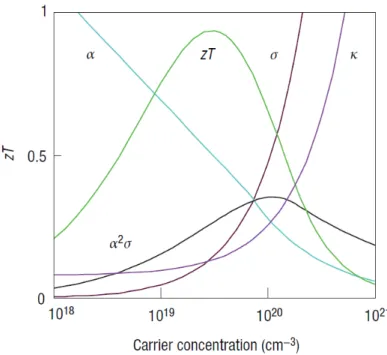
From the above introduction, we can realize that the high absolute value of Seebeck coefficient, the high electrical conductivity and the low thermal conductivity are required for achieving high ZT. A high absolute value of Seebeck coefficient ensures a large outputting EMF; a high electrical conductivity guarantees a low energy dissipation as Joule heating; a low thermal conductivity ensures a high and consistent temperature difference. Normally, power factor, i.e. 𝑆𝑆2𝜎𝜎, represents the figure of merit in the electrical part and can be tuned by doping. Form the calculation by G. Jeffrey Snyder and Eric S. Toberer5, it showed that the good thermoelectric materials are typically the heavily doped semiconductors with a carrier concentration between 1019 and 1020 carriers per cm3. The schematic illustration of optimizing ZT through carrier concentration tuning is shown in Figure 1.9.
Figure 1.8: Contribution of 𝜅𝜅𝑒𝑒𝑒𝑒 and 𝜅𝜅𝑝𝑝ℎto 𝜅𝜅𝑡𝑡𝑡𝑡𝑡𝑡𝑡𝑡𝑒𝑒for different types of materials.
Figure 1.9: The optimization of ZT through carrier concentration tuning. In the picture, α (0 to 500μV/K) represents the absolute value of Seebeck coefficient; σ (0 to 5000 S cm- 1) is the electrical conductivity; κ (0 to 10 W m–1 K–1) is the thermal conductivity5.
1.3 Thermoelectricity in thin films 1.3.1 Size effect
In the past decades, the progress of increasing the ZT of the thermoelectric materials was retarded owing to the interdependence of each parameter. As mentioned in section 1.2.1 and 1.2.2, if we enhance the electrical conductivity by doping, the suppression of the absolute value of Seebeck coefficient is accompanied; besides, the thermal conductivity also increases due to the contribution from increasing 𝜅𝜅𝑒𝑒𝑒𝑒. From this reason, ZT may decrease unexpectedly.
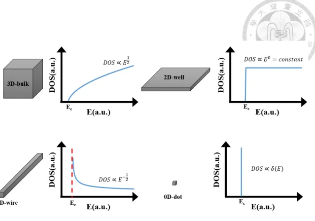
However, the emerging nanotechnologies offer opportunities to break through the current predicaments. By reducing the dimension of the materials, it shows a great potential to overcome the difficulty of the interdependence of parameters6. Since it is able to engineer the density of states for electrons straightforwardly without changing the composition elements. For example, it may destroy the high symmetric
characteristic of DOS in the Fermi window while the Fermi level goes deep into the conduction band, but still offers amounts of DOS. In this case, the high absolute value of Seebeck coefficient and the high electrical conductivity are obtained in the meantime.
The schematic diagram of the density of states for electrons in different dimension based on parabolic band structure is shown in Figure 1.10. Besides the benefits to electrical performance, the size effect also increases a large number of boundary
scatterings, which reduce thermal conductivity greatly, to reduce the thermal
conductivity. Overall, reducing the dimension of the materials is a promising way to enhance the figure of merit of thermoelectric.
1.3.2 Superlattice(Nanolaminates)
Thanks to the emerging nanotechnology, we can not only reduce the dimension of materials but also design and introduce some nanostructures into the materials, such as nanoinclusions7–12, nanopores13–16. Among these novel nanostructures, the superlattice (nanolaminates) shows a great ability to enhance the figure of merit, ZT17–22.
Nanolaminates are referred to the materials whose structures are made up of several kinds of base materials with different properties (e.g. composition elements, density, hardness and thermal conductivity.) alternatively and periodically in nanoscale. If the base materials are crystalline but in the different crystal structures, the nanolaminates can also be called as the superlattice. However, these two terms can replace with each other generally, so we use the term “superlattice” in this dissertation for convenience.
First, the complete and layered interfaces are able to suppress the thermal conductivity more effectively compared to the random distributed heterogeneous structure. As mentioned in section 1.2.3, the scattering centers inside materials retard the transport of phonons. For superlattice, when the interfaces are perpendicular to the
direction of heat transferring, the phonons with particular wavelength may undergo destructive interference completely according to the period length of interfaces.
Consequently, the contribution to thermal conductivity of the phonons with particular wavelength vanishes. Form this concept, we may filter out the phonons which offer major contribution to thermal conductivity by tuning the periodicity of interfaces even introducing multi-periodicity into the materials to reduce the thermal conductivity of superlattice effectively.
Second, the superlattice also offers an unparalleled way to overcome the entanglement of the electrical conductivity and the absolute value of Seebeck coefficient. Energy filtering effect, which can block the transmission of low energy carriers, occurs at the interfaces of two materials with the diverse transportation characteristic of charged carriers23–27. The schematic diagram of energy filtering effect is shown in Figure 1.11. Once again, the reduction of the absolute value of Seebeck coefficient is accompanied with the enhancement of electrical conductivity via doping, which makes the Fermi level goes deep into the conduction band for n-type materials.
However, if the energy barriers are placed along the transmitting direction of charged carriers, the low energy carriers no longer make contribution to the electrical
conductivity and Seebeck coefficient. Though the enhancement of electrical
conductivity is suppressed slightly, great mounts of carriers with energy higher than the
Fermi level still make positive contributions to Seebeck coefficient. For this reason the enhancements of the electrical conductivity and the absolute value of Seebeck
coefficient are obtained in the meanwhile. Owing to these advantages, the superlattice becomes the new paradigms in developing high ZT thermoelectric materials.
1.3.3 Advantages of thin film thermoelectric materials
As the growing usage of personal portable devices, the management and the recycling of waste heat in the ever-shrinking electronic devices have drawn much attentions nowadays. However, as the high performance bulk type thermoelectric materials are no longer suitable for the use in portable devices owing to the limited shape characteristic28–31. Therefore, the developments of nanoscale thermoelectric materials are demanded urgently. After years of effort, the progress in nanoscale thermoelectric materials has been made.
In the current results, nanowires32–35 and quantum-dots21,36–39 thermoelectric materials show excellent characteristics. Nevertheless, the packing density and the binding materials which provide the electrical conducting pathways and the mechanical strength still have to be taken into consideration in practical use. For this reason, the usages of extra materials and process are necessary to fabricate thermoelectric devices.
Hence, the usages of nanowire type and quantum-dot type thermoelectric materials to recycle the waste heat or cool the system increase the difficulty and complexity of the microminiaturized electronic device process.
On the other hand, the thin films thermoelectric materials, which also show promoted thermoelectric properties, are physically continuous and thus the complete materials, so the supporting materials are no longer required. In addition, the thin film deposition process are already utilized in the current semiconductor industry
extensively. Thus, the thin film thermoelectric materials are the best type of nanomaterials to recycle the waste heat and cool the system in microminiaturized electronic device. Among the current thin film deposition techniques, atomic layer deposition (ALD) shows a great potential for developing high performance thin film thermoelectric materials, since ALD is the emerging thin film deposition technique in semiconductor industry and possesses unparalleled the precise control over thickness and composition. These advantageous ensure the feasibility in practical use and the capability to fine tune the properties of deposited thin films.
Figure 1.10: The schematic diagram of the density of states for electrons in different dimension based on parabolic band structure.
Figure 1.11: The schematic diagram of energy filtering effect in superlattice.
1.4 Fundamental of atomic layer deposition and its advantages of depositing thin film thermoelectric materials
1.4.1 Atomic layer deposition(ALD)
Atomic layer deposition, which is a unique type of chemical vapor deposition (CVD), has drawn much attention in the recent years owing to its unique self-limiting growth characteristic. It utilizes two sequential self-limiting surface reactions between the vapors of precursors and the surface functional groups to deposit thin films. Take the deposition of Al2O3 as an example, the schematic illustration of film-growth mechanism is shown in Figure 1.12. The reaction steps are described as below:
(1) Trimethylaluminum, TMA, is introduced into reaction chamber and then reacts with the hydroxyl groups on the surface of substrate.
(2) The physisorbed TMA and the reaction byproducts, i.e. methane, are removed during N2 purge step.
(3) H2O is introduced into reaction chamber and then reacts with the surface methyl groups.
(4) Once again, the physisorbed H2O and the reaction byproducts are then removed during N2 purge step.
The TMA dose - N2 purge - H2O dose – N2 purge, these four steps are called as one cycle of ALD Al2O3 growth, which can form about 1 angstrom Al2O3. For growing
Al2O3 thin films, the reaction cycles are repeated until the desired thickness of Al2O3 are deposited.
Self-limiting, the unique characteristic of ALD reaction, makes the growth rate per cycle unchanged while increasing the dose amount of precursors and prolonging the purge time. This characteristic ensures following advantages: the defect-free deposition, the complete and uniform coverage over the surface with a high aspect ratio surface feature, the precise control over the film thickness and the elemental composition40.
Besides the selection of precursors, the deposition temperature also plays an important role to achieve self-limiting characteristic in ALD process. Since ALD growth only occurs within a particular temperature window (ALD window). The illustration of the dependence of growth rate per cycle on the temperature is shown in Figure 1.13.
When the temperature is below ALD window, there are two situations. One is that the precursors may condense on the surface easily, and then it causes a higher growth rate per cycle. The other one is that reactions between the precursor and the surface
functional groups are limited by the low kinetic energy, and then it cause a lower growth rate per cycle. On the other hand, when the temperature is above ALD window, there are also two situations. The first one is that the precursors may thermally decompose and the undesired reactions occurs, which raise growth rate per cycle. The second one is that the chemisorbed precursors tend to desorb form the surface, and then the lower growth
rate per cycle is obtained.
After years of effort, the deposition of various materials by ALD technique (e.g.
metal oxide41–43, metal nitride44–46, metal sulfide47,48, pure metal49) have been
demonstrated, and these thin films are successfully applied to varied applications, such as electronics, optoelectronics and biomedicine.
1.4.2 Molecular layer deposition(MLD)
Molecular layer deposition is a unique type of ALD. For traditional ALD, it focuses on the deposition of inorganic materials. However, MLD is referred to the deposition of pure organic polymers or organic-inorganic hybrid materials. Similar to ALD, MLD is also composed of two sequential self-limiting reactions. The deposition of pure organic polymers (e.g. polyamide, polyester and polyimide) have been
extensively studied50–53. Here, we take the deposition of polyester as an example to illustrate the growth mechanism. The schematic illustration is shown in Figure 1.14. In the first step, multifunctional carboxylic acid is introduced into the reaction chamber and then reacts with the surface hydroxyl groups. In the following N2 purge step, the excess unreacted monomers and the reaction byproducts are removed. Next, polyol is introduced and reacts with the surface carboxyl groups. In the last step, N2 purge the
surface to remove the excess unreacted polyol and the reaction byproducts. These four steps compose one cycle of MLD polyester growth.
As mentioned before, MLD is also developed to deposit organic-inorganic hybrid materials. The most iconic one is metalcone54–57. Take the deposition of alucone as an example, the reaction mechanism is almost as the same as the one of ALD Al2O3, the only one difference is that the polyol substitutes for H2O to reaction with the surface methyl groups and offers the surface hydroxyl groups. After cycles of MLD alucone
deposition, organic-inorganic hybrid material with special linkage Al
O R
O n is formed.
From the aspect of the growth mechanism, ALD and MLD are compatible to each other by selecting particular precursors with proper functional groups. Owing to the great control of composition, i.e. ratio of organic parts to inorganic parts, the
combination of ALD and MLD techniques is not only simplify the manufacturing process of organic-inorganic multilayer hybrid materials but also able to fine tune the characteristics (e.g. hardness, refractive index, gas permeability and thermal
conductivity) of the deposited hybrid materials58–61. The detailed introduction to applications of ALD/MLD superlattices (or nanolaminates) other than thermoelectric are stated in section 1.6.
1.4.3 Advantages of ALD on depositing thin film thermoelectric materials
As mentioned in section 1.2.4, the doping is a general technique to enhance the electrical conductivity of a semiconductor. However, a precise control of doping level is required to find out the best combination of electrical conductivity and Seebeck
coefficient, which offers the highest power factor (PF), i.e. σ × 𝑆𝑆2. Thanks to the layer- by-layer growth in atomic scale, ALD technique offers an unparalleled precise control of element concentrations, which is able to fine tune electrical conductivity, over other thin film deposition techniques. In addition, the layered and complete host-guest heterogeneous interfaces inside the superlattice are believed to impede the transport of phonons in materials effectively due to the severe phonon scatterings which are resulted from the phonon transportation property difference between the host material and the guest material (e.g. density, vibrational constant and coordination). Hence, the thermal conductivity of a material with the layered distribution of guest material decreases more drastically compared with the one with random distribution. Moreover, the ability to fine tune the thickness of entire film and basis materials is able to bring the size effect and the energy filtering effect into full play. Besides, attributed to the fine integration of ALD and MLD deposition process, the novel organic-inorganic superlattices are able to be deposited, and thus thermoelectric properties of them can be explored. With these
advantages, ALD and MLD are the promising techniques to develop the thin film thermoelectric materials.
Figure 1.12: The schematic illustration of ALD film growth mechanism.
Figure 1.13: ALD window, the dependence of growth rate per cycle on temperature.
Figure 1.14: The schematic illustration of MLD polyester film growth mechanism.
1.5 Literature review of thin film thermoelectric materials deposited by ALD
To date, the depositions of several traditional bulk type thermoelectric materials by ALD have been successfully demonstrated. Bi2Te3/Sb2Te3 superlattices were
deposited by Nminibapiel et al.62 The deposition of PbTe/PbSe superlattice was reported by Zhang et al.63 and Sarnet et al. also demonstrated the deposition of Bi2Te3 by the usage of the novel synthesized in-house precursor (Et3Si)2Se64. Recently, Bi2S3 was also deposited by Mahuli et al65. However, few selections of precursors suppress the
tunability of process, and then make it hard to fine tune the properties of materials.
Moreover, the low reactivity (e.g. BiCl3 and SbCl3) and the low volatility (e.g.
lead(II)bis(2,2,6,6-tetramethyl- 3,5-heptanedionato), Pb(C11H19O2)2 and bismuth(III) bis(2,2,6,6-tetramethylheptane-3,5-dionate), Bi(thd)3) precursors also reduce the robustness and reproducibility of the ALD processes. Besides, the traditional bulk type thermoelectric materials are disputed owing to containing scarce and toxic elements.
Therefore, the traditional bulk type materials are not able to exert the potential of ALD (e.g. fine tune the electrical conductivity via doping process and the period length of superlattice) and then are used as next the generation thin film thermoelectric materials.
Hence, it is important to choose a robust test-vehicle material to verify the advantages of ALD in developing thin film thermoelectric materials systematically.
ZnO (zinc oxide), which is earth abundant, environmental friendly, suitable band gap and crystal structure (direct band gap ~3.3ev at 300K and hexagonal wrutize structure), has been considered to be the next generation thermoelectric material. The thermoelectric properties of ZnO fabricated by traditional ways (e.g. sputtering, sol-gel and powder sintering) have been extensively studied. Moreover, its ALD process is already well established and applied to varied applications, such as thin-film transistors66,67, transparent conducting oxide68,69, gas sensor70,71, the electron transporting layers in OPVs72,73. Hence, ZnO is promising in demonstrating the capability of ALD in the thin film thermoelectric materials. The Table 1.1 summarizes the current progress in ALD ZnO thin film thermoelectric materials. Among the current results, Gallium showed best doping efficiency, the electrical conductivity after doping was promoted to 1808 S/cm at 1% Ga doping concentration. For enhancing the absolute value of Seebeck coefficient, organic-inorganic superlattice, i.e. 4,4'-
Oxydianiline(ODA)/ZnO, deposited by ALD/MLD combination achieved the best Seebeck coefficient, -220 μV/K. However, the thick Al2O3 dopant layers (0.82nm) inserted into ZnO matrix suppressed the thermal conductivity and enhanced the ZT value most effectively, the values are 0.26 W/m K and 0.14, respectively.
Table 1.1: The current progress in ALD ZnO thin film thermoelectric materials.
Dopants Doping concentration
(%)
Electrical conductivity
(S/cm)
Seebeck coefficient
(μV/K)
Thermal conductivity
(W/m K)
ZT
(300K) Ref
Ga 1 1808 -60 N/A N/A 74
Al 2 107 -63 1.18 0.012 75
Al 2 278 -66 0.26 0.14 76
ODA/
HQ/
AP
2.5 1.6/
3.5/
10
-220/
-205/
-160
N/A N/A 77
Al & HQ 2 14.3 -200 N/A N/A 78
1.6 Applications of ALD/MLD superlattices
As stated in section 1.4.2, the combination of ALD and MLD techniques possesses a great control of the composition, structure of superlattice, so it is easy to fine tune the characteristics of deposited superlattice materials, such as hardness, refractive index/
extinction coefficient, flexibility and conductivity. Therefore, there are plenty of researches about the application of superlattices materials deposited by ALD/MLD techniques, including Lithium-ion battery, filtration, gas separation, gas molecule capture/release and optical fiber79–85. Here, we only focus on the following two applications, flexible high performance gas barrier and nanoporous materials.
1.6.1 Flexible high performance gas barrier
In recent years, flexible/stretchable electronics have drawn much attention and their potentials on a variety of applications have been demonstrated successfully, such as wearable devices, artificial skins, diagnosis and therapy of movement disorders.
However, the commercialization of flexible/stretchable electronics is greatly hindered by the lack of effective encapsulation with satisfying flexibility/stretchability. To address this issue, our group have verified the feasibility of depositing superlattice- based flexible high performance gas barrier through ALD/MLD techniques. In our results, the inserted polymer, PA32 (Poly(imino-(1,3-dioxotrimethylene)-
iminoethylene)) (the structure Figure 1.15), provided the flexibility and decoupled the defects of inorganic parts, Al2O3 and/or HfO2, and thus the gas-barrier performance was promoted by prolong the torturous paths of gases. The schematics of the torturous path of inorganic-organic multilayer gas barrier is presented in Figure 1.16. Under the optimal structure, the WVTR (water vapor transmission rate) was ~10-6 g m-2 day-1, which meets the requirement of encapsulation of OLED, even with 10% strain. For the detailed results, they can be seen in the doctoral dissertation of Ming-Hung Tseng, Ph.D.
C O
C N H
O H N
n
Figure 1.15: The structure of PA32.
Figure 1.16: The schematics of torturous path of inorganic-organic multilayer gas barrier.
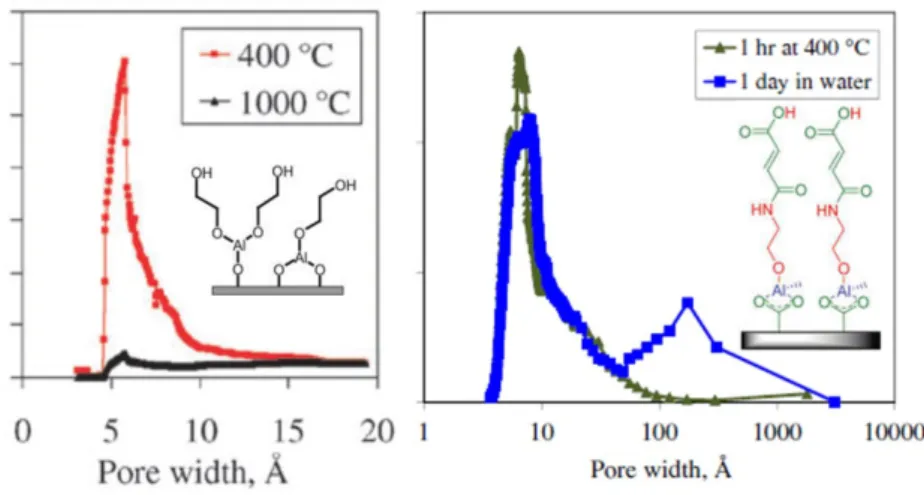
1.6.2 Nanoporous materials
In the past, the fabrication of nanoporous materials, such as zeolite and metal organic framework, required a series of chemical reactions with delicate and precision control; hence the practicality is greatly limited. Luckily, the evolution of ALD/MLD superlattice provides a novel route to fabricate nanoporous materials, whose pore size is smaller than 1 nm especially. To form nanoporous materials, the metalcone-type
superlattice films, including alucone, zincone, titanicone, are post-annealed in oxygen contained atmosphere at an elevated temperature (above 400°C) to eliminate the carbon- segments, thus the nanoscale pores are obtained with varied metal oxide scaffolds based on the selected metalcone. On the other hand, the conductive-carbon contained metal oxide is obtained by annealing the deposited superlattice films in the inert atmosphere.
The schematic illustration of the evolution of ALD/MLD superlattice after post- annealing in various atmosphere is shown in Figure 1.1779. In the process of forming nanoporous materials, the pore size and porosity are determined by the thickness (chain length) and periodicity of organic segments. Therefore, these properties can be fine- tuned by selecting a proper organic precursor and designing a certain structure of
superlattice. The tunability of pore size is presented in Figure 1.18 by the integrating the researches done by Liang et al86,87. So far, the resulted nanoporous materials with varied pore size have been utilized in a variety of researches, e.g. the ion-conductive protection
layer of electrode in Lithium-ion battery, the molecular sieve in gas separation and filtration of organic molecules, stabilizer for enhancing Pt ORR performance and the controlled release of molecules.
Figure 1.17: The schematic illustration of the evolution of ALD/MLD superlattice after post-annealing in various atmosphere.
Figure 1.18: The tunability of pore size resulted from ALD/MLD superlattice.
1.7 Motivation and objective statements
As mentioned in section 1.3.3. , the demand of thin film thermoelectric materials is called for owing to the growing attention in the waste heat recycling and the cooling system in personal portable devices. Thanks to the advantages, such as the precise control over the thickness and the composition of thin films, the conformal coverage over large area substrates with high ratio surface features, ALD is the best technique to deposit the high performance thin film thermoelectric materials.
To date, the progress of ALD ZnO-based thin film thermoelectric materials has been made significantly. By fine tuning the thickness of Al dopant layers, the ZT value of has been enhanced by almost two orders of magnitude, i.e. 0.0015 to 0.14. However, from Table 1.1, we can discover that only few kinds of dopants were utilized in current researches, e.g. Al and Ga. Also, only single periodicity of superlattice was designed to reduce the thermal conductivity of materials via interface scattering in each research.
Moreover, the organic insertions were limited to monolayers formed by benzene ring contained molecules which are almost insulation, so the current ALD/MLD organic- inorganic superlattices showed the terrible electrical conductivities. Hence, more detailed and fundamental researches have to be done in order to verify the feasibility and show the advantages of ALD technique in developing the high performance thin film thermoelectric materials. The researches include the type of dopants and the
formed interface, the dependence of thermal conductivity on interface period length, and development of nanoscale conducting polymers and their superlattice with inorganic materials.
As for the flexible high performance gas barrier, although the superlattice, which was composed of HfO2 and PA32, showed an unprecedented gas barrier performance, it still suffered from the issue of the long term stability due to the hydrolysis of PA32;
hence, the performance decayed with the time exposed to water. To address this issue, the development of anti-hydrolysis polymers as the substitutions for PA32 in the deposition of superlattice is crucial to improve the long term stability of superlattice.
Regarding the progression of nanoporous materials, the way to eliminate organic component was post-annealing at an elevated temperature, basically above 400°C.
Therefore, it is hard to use with the flexible polymer-based substrates and/or integrate with other organic-based devices since the elevated annealing temperature can also pyrolyze them. Hence, the exploration of the low-temperature pyrolysis process of metalcone superlattices can enhance the practicability of metalcone-resulted nanoporous materials.
In this dissertation, our objectives focus on the following four exploratory studies to improve the performance of superlattice thermoelectric materials, ALD/MLD gas barrier.
(1) Study of the effects of composition and structure on the thermoelectric properties of metal oxide superlattice thin films.
(2) Study of the effects of incorporating O18 isotope into the metal oxide superlattice on its thermoelectric properties.
(3) Development of novel MLD conducting polymers and their superlattice with metal oxide semiconductors.
(4) Development of anti-hydrolysis polymers by MLD technique and the fabrication of long-term stable gas barrier composed of metal oxide and anti-hydrolysis
polymers.
1.8 Research approach
1.8.1 High valence and high atomic weight metal ion doping
Typically, the doping of metal oxide is conducted by introducing guest ions (dopants) which are aliovalent to replace the cations or anions in the host materials. In ALD technique, the guest oxide layers, in which metal ions are aliovalent compared with the ones in host materials, are periodically inserted into the host metal oxide to offer dopant ions. Take Al doped ZnO (Al:ZnO) as an example, Al2O3 guest layers were periodically inserted into ZnO host layers by alternating one Al2O3 cycle with a number of ZnO cycles. In this case, since the valence of dopants, i.e. Al3+, is higher than that of Zn2+, the free electrons, which are able to make contributions to conducting, were created at the interface of Al2O3 and ZnO; hence the n-type doping was achieved. In addition to inducing free electrical carriers, the insertion of guest layers created a number of host/guest interfaces periodically which can also serve as the phononscattering centers to reduce the thermal conductivity of Al:ZnO by increasing interfacial scattering.
As listed in Table 1.1, the current ALD researches about thermoelectric properties of doped ZnO thin films focused on the usage of boron-group metal oxides, i.e. Al2O3
and Ga2O3, as inserted guest layers to arrive at n-type doping and reduce thermal conductivities by increasing interfacial scattering. However, based on the concept of

![HPSH [ 氧化數平衡反應式係數 ]](data:image/gif;base64,R0lGODlhAQABAIAAAP///wAAACH5BAEAAAAALAAAAAABAAEAAAICRAEAOw==)