國立臺灣大學工學院材料科學暨工程研究所 碩士論文
Institute of Materials Science and Engineering College of Engineering
National Taiwan University Master Thesis
摻雜錳之矽酸鋅/氧化矽殼/核微球之合成與光閘晶體(PBG)光 譜之分析
Synthesis of Mn-doped Zn
2SiO
4/SiO
2core-shell structure and characterization of photonic band-gap crystal (PBG)
謝函育 Hsieh, Han-Yu
指導教授:韋文誠 博士 Advisor: Wei, Wen-Cheng, Ph.D.
中華民國 97 年 7 月
July, 2008
致謝 時光飛逝,碩士生涯即將結束。
在台大的這段時間,承蒙了許多人的教導、幫忙、以及支持。首先要感謝的 韋老師,能孜孜不倦的教育學生無論是在課業、生活、或是待人處世各方面。在 即將畢業的這段期間,更是要常常麻煩老師晚上或是假日加班改論文,真是辛苦 了。同時要感謝擔任口試委員的黃啟原老師、劉如熹老師和林清富老師對於我論 文中的疑問或是缺失給予寶貴的意見和指教。
在Wei group 中,頌恩學長是最萬能最樂於幫忙的,感謝學長無論是在實驗、
課業的幫忙(對了還有體育活動);邦英學姐同樣是很樂意幫忙,感謝學姐在TEM
和XPS 實驗的協助,同時也祝福學姐在結婚之後要更幸福喔;浚傑學長與我相處
的時間比較少,不過浚傑學長在做人處世的積極態度一向是讓我相當欣賞的;一 中學長在實驗室的時間不長,但只要是學長能力範圍之內,向他開口沒有不答應 的;右儒學長則是擔任我一年級時的小老師,以前遇到問題常常就先想到找右儒 學長討論;銘璁和佳明學長也經常在做實驗或是功課上給我建議;家嘉和哲彥則 是一齊打拼和互相加油的好夥伴;怡如和嬿雯兩個可愛的學妹給實驗室添加了許 多的活力,同時也平衡了實驗室的陽剛之氣;士岳、勤文、敬閎還有智淵,以後 也要在課業和實驗上繼續加油。
感謝系上辛苦的行政人員,林由莉小姐、張瑛梅小姐、周麗美小姐、李玉玲 小姐、李苑慈小姐、陳學人先生、高崇源先生等等,有你們的幫忙使我能順利完 成學業。感謝貴儀的蔡錫昌先生、凝態中心的張秀如學姐、鶯歌陶瓷中心的沈俊 良先生、陳彥涵小姐、東元奈米應才的方金壽博士,有你們的幫忙讓我的論文更 完整。
感謝平時幫我加油打氣還有分享心情的好朋友們,彦亨、宜蓉、小羽、黃小 曼、奇勲,還有族繁不及備載的大同高中、成大材料的同學們;感謝台大材料系
壘的學長同學學弟們,我會記住和你們一起在2007 年拿下台大盃冠軍的榮耀。
最後感謝我的家人,爸爸媽媽,能夠一直支持我,謝謝。
摘要
摻雜錳之矽酸鋅(Mn-doped Zn2SiO4)是一種具有高亮度綠光放射(520 nm)的光
致發光和陰極發光之螢光材料。在本篇研究中,我們嘗試了六種方法製備矽酸鋅 螢光粉。其中ZSpII和ZSpVI具有最好的效果。以膠粒製程和強迫析出法製備氧化 矽/矽酸鋅核殼組成之膠體溶液。鋅離子和錳離子會鍍膜於氧化矽顆粒。在乾燥和 熱處理之後,在表面析出之鋅/錳離子會與氧化矽反應成為矽酸鋅結晶相。鋅/錳離 子的析出行為以感應耦合電漿-原子放射光譜(ICP-AES)做分析;核殼之微結構則由 電子顯微鏡做分析;結晶相由X光繞射儀鑑定;光致發光及陰極發光由光譜儀測 量。實驗結果顯示隨著熱處理溫度上升,析出物首先形成氧化鋅,並與氧化矽反 應形成矽酸鋅結晶。最後可得到由矽酸鋅鍍膜於具有光子晶體特性的氧化矽模 版。此外,矽酸鋅粉末也製作成漿料塗佈於透明電極以作為陰極發光元件,同時 對於此元件之光學表現做分析。
關鍵字︰光子晶體、核殼/結構、螢光粉、摻雜錳之矽酸鋅、膠粒製程、光致發光、
陰極發光
Abstract
Manganese doped zinc silicate (Zn2SiO4:Mn) is a kind of phosphor materials that has a photoluminescent (PL) (at 520 nm) and cathode-luminescent (CL) properties with relative high intensity green light emission. In this study, six methods were tried to synthesis Zn2SiO4 powder. Two (ZSpII and ZSpVI) methods have the best performance.
The colloidal particle consisted of SiO2 core-Zn2SiO4:Mn shell has been synthesized via colloidal process and forced precipitation. The reactants Zn/Mn ions were coated on the SiO2 particles. After drying and calcination, the Zn/Mn precipitates reacted with SiO2, then transformed to Zn2SiO4 phase. The behavior of Zn/Mn ions precipitation on silica spheres were studied by ICP-AES. The morphology of core-shell structure was investigated by electron microscopy. The phase identification was studied by X-ray diffraction. The PL and CL properties were determined by photon spectrometer. The results showed that with the increase of annealing temperature, the precipitates formed ZnO first, then reacted with SiO2 and transformed to Zn2SiO4 phase. Finally, SiO2
template with PBG structure coated by ZnSiO4:Mn shell was obtained. Besides, Zn2SiO4 powders as a paste coated on transparent electrode for assembling a CL device.
The performance of the device was characterized as well.
Keywords: PBG, core-shell, phosphor, Mn-doped Zn2SiO4, colloid, photoluminescence, cathode-luminescence
Content
摘要 ... I Abstract ... II Content ... III List of Figures ... V List of Tables ... X
Chapter 1 Introduction ... 1
Chapter 2 Literature Review ... 4
2.1 Photonic Band-Gap Crystals ... 4
2.1.1 Basic Concepts of Photonic Band-Gap Crystals ... 4
2.1.2 Assembly of Photonic Band-Gap Crystals ... 6
2.2 Luminescence Properties ... 19
2.3 Synthesis of Core-Shell Structures ... 28
2.3.1 Hydrothermal Method ... 29
2.3.2 Layer-by-layer Method ... 29
2.3.3 Osmotic Swelling ... 30
2.3.4 Sol-gel Method ... 31
2.3.5 Water/oil/water (W/O/W) Emulsion ... 32
2.4 Synthesis of Zn2SiO4:Mn Material ... 38
2.4.1 Zn2SiO4 Powders ... 39
2.4.2 Zn2SiO4 Thin Film ... 42
Chapter 3 Experimental Procedure ... 52
3.1 Materials ... 52
3.2 Experimental Design ... 52
3.3 Sample Preparations ... 53
3.4 Characterization ... 56
3.4.1 Phase Identification by XRD ... 56
3.4.2 Thermal Analysis by DTA ... 56
3.4.3 Zeta Potential Measurement ... 57
3.4.4 Microstructural Analysis by SEM/EDS and TEM ... 57
3.4.5 Chemical Composition Analysis by ICP-AES and XPS ... 58
3.4.6 Luminescence Property Analysis ... 59
Chapter 4 Results ... 66
4.3 Microstructure Observations and EDS Measurements ... 81
4.4 Luminescence Property ... 91
Chapter 5 Discussions ... 104
5.1 Methods Comparison ... 104
5.2 Effects of Mn2+ to PL Property ... 117
5.3 PBG Effects to PL Property ... 127
Chapter 6 Conclusions ... 131
Reference ... 133
List of Figures
Fig. 1- 1 Schematic diagrams illustrating PBG crystals with 1-D, 2-D and 3-D
dimensional structure. --- 3 Fig. 2- 1 Images showing the natural PBG structures. The top one is an opal and the
bottom ones are a butterfly and enlarged structure. ... 12 Fig. 2- 2 A typical band-gap diagram representing a PBG crystal with diamond
structure. The components are in spherical shape and have a dielectric constant of 12. ... 13 Fig. 2- 3 Schematic diagram that illustrates the silica glass tubes constructing a
2D-PBG crystal structure into fiber with the furnace operating at about
1800-2000oC. ... 14 Fig. 2- 4 SEM image illustrating the microstructure of a success waveguide consist of
12 stacked layers with a period of 4 μm. The designed waveguide itself is
sandwiched by the upper and lower complete PBG crystals. ... 15 Fig. 2- 5 A schematic diagram illustrating the behavior of particles by solvent flow
along upward direction. Both clear and obstructed niches are possible packing sites for the moving particles. ... 16 Fig. 2- 6 A potential diagram representing the net force resulting from summation of
repulsive force (electric double layer) and attractive force (ven der Waals force).
... 18 Fig. 2- 7 Structure of an EL device. The thickness of the phosphor layer in this case is
about 700 nm. ... 26 Fig. 2- 8 A schematic diagram showing EL mechanism in an EL device. ... 27 Fig. 2- 9 Schematic diagram indicating the processing steps to prepare hollow
core-shell particles with layer-by-layer method. ... 34 Fig. 2- 10 TEM micrographs showing the (a) (SiO2/PDADMAC)2-coated PS latex
particles and hollow silica spheres after calcination with (b) one, (c) two and (d) three layers coating. ... 35 Fig. 2- 11 Schematic diagram illustrating a sol-gel reaction resulting in the products of
different morphologies. ... 36 Fig. 2- 12 Schematic diagram representing the reaction steps of W/O/W emulsion. ... 37 Fig. 2- 13 Crystal structure of willemite unit cell in this diagram represents the
positions of Zn (dark balls), Si (light balls), and O (small balls) ions in this system.
spectra of Zn2SiO4:Mn was coated as a thin film on wafer... 46 Fig. 2- 15 TEM images showing the Zn2SiO4:Mn made by Ahmadi’s method contains
both the spherical and acicular shape. ... 47 Fig. 2- 16 Phase diagram of ZnO-SiO2 system. ... 48 Fig. 2- 17 DTA results of the ZnO-SiO2 mixture with LiF (left) and without LiF (right).
The reaction temperature was reduced by adding flux (LiF in this case) into the system. ... 49 Fig. 2- 18 Two EL spectra showing the emitting brightness and efficiency versus
applied voltage of Zn2SiO4:Mn with adding LiF as a flux. ... 50 Fig. 2- 19 X-ray diffraction analysis of the samples illustrating phase transformation
temperature. The annealing temperatures varied with (a) 800oC, (b) 840oC, (c) 920oC and (d) 980oC. ... 51
Fig. 3- 2 Experimental flowchart of this study. ... 62 Fig. 3- 3 A schematic diagram of a CL device. CNT electrode acted as a field emission
electron source. The electrons accelerated by applied DC power source then stroke on phosphor layer and thus generated light. ... 63 Fig. 3- 4 Schematic diagram of particles in G1 glue on a Cu grid. ... 64 Fig. 3- 5 Image showing the fluorescent spectroscopy system with (a) sample cell, (b)
detector (with optical fiber), (c) fluorescent spectrometer, (d) optical fiber connected to UV source, and (e) computer. The white circle is a cavity where samples could be placed in. ... 65 Fig. 3- 6 Block diagram representing the setting of PL measuring. ... 65
Fig. 4- 1 The measured contents of Mn2+ doping from calcined Zn2SiO4:Mn particles analyzed by ICP-AES. The unit is defined as molar percent of Mn/Zn. ... 70 Fig. 4- 2 Titration curves of [Zn2+] and [Mn2+] versus pH of solutions, respectively. ... 71 Fig. 4- 3 Titration curve of 0.5 ml 0.1M Zn(NO3)2 dissolved in 20 g de-ionized water
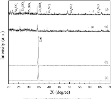
titrated by NaOH(aq). The dash line is the first order derivative curve of the titration curve. ... 72 Fig. 4- 4 Zeta-potential of calcined Zn2SiO4:Mn particles as a function of pH value.... 73 Fig. 4- 5 XRD patterns of Zn2SiO4:Mn (5 mol% doping) particles varies with different
heat treatments of 1200-500oC from top to bottom, respectively. ... 77 Fig. 4- 6 DTA curve representing the ZSpII samples annealing at 500oC for 2 hr. ... 78 Fig. 4- 7 SEM images of ZSpII bulky samples after heat the treatment at (a) 1100oC and
(b) 1200oC for 2 hr. ... 79 Fig. 4- 8 XRD pattern of Zn2SiO4:Mn powders dispersed in basic solution showing the
possible phases. The arrows pointed out the extra peaks other than those belonging to Zn2SiO4 phase. ... 80 Fig. 4- 9 SEM images showing the morphologies of (a) silica particles prepared by
Stöber method, (b) silica particles coated with Zn2+ and Mn2+ before calcinations, and (c) dried and after 1100oC calcination for 2hr. ... 84 Fig. 4- 10 SEM image showing silica particles with PBG structure at 1000oC heat
treatment for 2 hr. The precursors consists of TEOS:NH4OH:C2H5OH = 10:20:200.
... 85 Fig. 4- 11 SEM images of SiO2-template coated with Zn and Mn solution (a) original
concentration, or diluted by ethanol in volume to (b) 2, (c) 3, (d) 5, (e) 10 and (f) 20 times, then dried and annealed at 1000oC for 2 hr. The white circles illustrate that there are still a little amount of non-uniform coating, however, this
non-uniform coating did not exist at all as the precursors were diluted to 3 times. 86 Fig. 4- 12 SEM images of coated SiO2-template by the Zn/Mn solution diluted with
alcohol to 5 times. The samples were dried and annealed at (a) 600oC, (b) 800 oC, (c) 1000 oC, and (d) 1200 oC, respectively. ... 87 Fig. 4- 13 SEM image showing the positions of EDS measurement on ZSpVI sample. 88 Fig. 4- 14 TEM images showing the detail morphologies of assembled SiO2-template
with (a) one layer and (b) two layers packing, respectively. ... 89 Fig. 4- 15 TEM cross-sectional view of SiO2 particles coated with precursors (a)
directly and (b) diluted by alcohol to 5 times, respectively. ... 90 Fig. 4- 16 Optical spectrum of the UV source which was used in this study. ... 95 Fig. 4- 17 Photos of samples (a) and (b) prepared via ZSpII, and (c) and (d) via ZSpVI
processes. (a) and (c) were exposed under visible light while (b) and (d) were exposed under 254 nm UV light. ... 96 Fig. 4- 18 PL spectra of ZSpII intensity with different amounts of Mn ion doping. The
doping ratio of Mn was defined as Mn/Zn. ... 97 Fig. 4- 19 Spectra illustrating the PL intensity of ZSpII sample annealed at different
annealing temperatures. The samples of 1000oC and 1100oC perform a better emission property, while the intensity decreased if the temperature rose up to 1200oC. ... 98
Fig. 4- 21 PL spectra of ZSpVI samples diluted by ethyl alcohol to specific
concentration, then annealed at 1000oC for 2 hr. ... 100 Fig. 4- 22 Photos showing CL device in a vacuum chamber. ... 101 Fig. 4- 23 I-V curve illustrating the electrical property of ZSpII sample assembled in
TECO/CL device existed by a threshold voltage at 175 V and saturated at 310V.
... 102 Fig. 4- 24 CIE analysis result of ZSpII sample in TECO CL device. The sample of
studied is located at x = 0.2899 and y = 0.5048, which corresponds to the circle in this diagram. ... 103
Fig. 5- 1 XRD patterns illustrating the Zn2SiO4:Mn particles prepared by solid state reaction. The patterns were arranged by different annealing temperatures from 900-1200oC for 2 hr (bottom to top). ... 108 Fig. 5- 2 XRD patterns illustrating the Zn2SiO4:Mn particles prepared by solid state
reaction, which samples were ground and re-annealed for one to three times at 1100oC for 2 hr. ... 109 Fig. 5- 3 Photos showing the Zn2SiO4:Mn disks (1100oC for 2 hr) exposed (a) without,
and (b) with applied 254 nm UV light, where the left piece and right ones were synthesized via solid state reaction and colloidal process, respectively. ... 110 Fig. 5- 4 PL spectrum of the emission intensity of Zn2SiO4:Mn disks prepared by solid
state reaction (ZSpV series) and solution process (ZSpII). All of these samples were annealed at 1100oC for 2 hr. The number following the sample notation (ZSpV) is the cycles of grinding and re-annealing for one (square), two (circle) and three (triangle) times. ... 111 Fig. 5- 5 SEM image showing irregular shape of Zn2SiO4:Mn powder (ZSpV)
synthesized via solid state reaction at 1000oC for 2 h. ... 112 Fig. 5- 6 SEM image showing ZSpI samples annealed at 1000oC for 2 hr. The Zn and
Mn ions precipitated randomly, instead of uniformly coating on SiO2 particles surface. ... 113 Fig. 5- 7 XRD patterns showing crystalline phase of ZSpIII powder series after
quenching (top) and 800oC annealing (the other two patterns). The product
contained not only Zn2SiO4, but also a Zn4O(BO2)6 phase. ... 114 Fig. 5- 8 SEM images showing the morphology of ZSpIII series after calcination at
800oC for (a) 5 hr and (b) 10 hr, where (a2) and (b2) were imaged under BSE mode. X area is Zn rich region; while Y area is B rich region. The black area is
pores that are resulted from crystallization in the glass. ... 115 Fig. 5- 9 XRD patterns showing the crystalline phase of ZSpIV annealed at 400oC for 2 hr. The crystalline phase is indexed as Na2ZnCl4(H2O)3. ... 116 Fig. 5- 10 Schematic diagram explaining Zeeman effect, where is frequency, e is
electron charge, m is mass, and B is the magnetic field. The transition states exists only when Δml = 0 and ±1, and the phenomenon had been proven by the
Stern-Gerlach experiment. ... 122 Fig. 5- 11 Energy of d orbital of transition metal ions with (a) ion in octahedral site or
tetrahedral site with weak crystal field, where (b) represented the case of electron configuration of (e)2(t2)3 and (t2)5, respectively. ... 123 Fig. 5- 12 Schematic diagram showing the variation of energy level while Mn2+ is
adsorbing or releasing energy by light. ... 124 Fig. 5- 13 XPS spectra illustrating the binding energy of Mn ions. The samples
calcined at 1100oC for 2 hr were doped with 5 mol% (top) and 50 mol% (bottom) Mn (based on Zn). Both of the maximum peaks located at 641 eV. ... 125 Fig. 5- 14 SEM images of ZSpVI samples in random (top) and ordered (bottom)
packing, respectively. Both of the samples were annealed at 1000oC for 2 hr. .. 129 Fig. 5- 15 PL spectra of ZSpVI samples with and without PBG structure. The sample
that was ordered packing performed a stronger PL intensity (about 70%) greater than the other one. ... 130
List of Tables
Table 2- 1 A list showing the IEP point of some ceramic materials ... 17 Table 2- 2 Green phosphors that have been used for optical instruments and their
performance. ... 24 Table 2- 3 Radii of some ionic species existed in crystals with CN = 4 ... 25 Table 3- 1 List of methods tried in this study. ... 61 Table 5- 1 List of binding energy belonging to different valence states of Mn. The unit
in this table is eV and the spectrum considered in this case is 2p3/2. ... 126
Chapter 1 Introduction
Photonic band-gap crystals with a structure similar to opal which composes of materials arranged in periodic way has been discovered over 15 years. The characteristics of a PBG crystal (Fig. 1- 1) appear band gap that could fully reflect electromagnetive wave [1]. Opal that constructed by silica particles is a nature PBG crystal. Some materials, e.g. TiO2, and CdSe have also been tried to assemble a PBG crystal. If silica particles are substituted by phosphoric materials, we may improve photoluminescence property of the assembled crystal.
Different kinds of phosphor materials are widely used for illumination and display.
Televisions, fluorescent lamps, neon lamps, cathode ray tube (CRT) monitors field emission display are the most common products that use phosphors. Fluorescent lamp is a typical example that contains electrodes which supply electrons as applied with high voltage. These electrons strike mercury vapor and thus emit UV light. Phosphor coating on the lamp adsorbs the UV spectrum and emits visible light. The lamps, which are operated with phosphors and excited by UV light, perform at a higher efficiency and low heat. The phosphor materials used in the past 3 decades include tungstate (WO32-), phosphate (PO43-) or halide (X-). Oxide and rare-earth based oxide with Tb, Sm, and Ce
Phosphors can be classified into several categories: organic phosphors, inorganic phosphors, and radioactive phosphors. Organic phosphors are synthesized by polymer and affected by different substitutional function groups, sites, and activators. Inorganic phosphors are activated by the electrons in the orbits, or by rare-earth or transition oxides which are excited and relaxed between band gaps. Radioactive phosphors are capable of emitting light spontaneously by the energy releasing from radioactive element so to activate phosphors.
Ceramic-based, organic or sulfate-based phosphors are compared, the oxide-based phosphors have good luminescent characteristics, high chemical stability and good resistance against moisture. Therefore, ceramic-based phosphors operate and last longer life time. So oxide-based phosphors become more popular in display industry. [3, 4]
The objectives of this study are to (1) synthesize spherical submicron sized particles with a SiO2 core-Zn2SiO4 shell structure, (2) construct a PBG crystal with the core-shell particles and measure the optical (PL and EL) properties of the products, and (3) design a device that allows the phosphor performing luminescent property.
Fig. 1- 1 Schematic diagrams illustrating PBG crystals with 1-D, 2-D and 3-D dimensional structure. [2]
Chapter 2 Literature Review
2.1 Photonic Band-Gap Crystals
2.1.1 Basic Concepts of Photonic Band-Gap Crystals
As a general knowledge, a material with components or atomic elements arranged in a periodic way could be named as a crystal. Salt or so called NaCl is a typical example that represents a crystal with face centered cubic (FCC) structure, which Na+ and Cl- situated one by one and have a coordination number of 6. The same concept could be finely describing the photonic band-gap (PBG) crystals. The crystal structure such as FCC or else, is defined by how the elements packing in the system. However, the scale of PBG crystals in this topic is much larger than the traditional crystal structure. In other words, the size of the elements (particles or components) which are used to construct a PBG crystal ranged from submicron to micron size.
Opals and wings of some insects are the examples that have nature PBG structure [5]. Opals are the minerals full of spherical submicron silica particles. The colorful surface is resulting from the geometric structure of the silica particles which back- scatters the light of specific spectrum, instead of the original white color of the silica surface, as Fig. 2- 1. With the different band-gaps, the color would be varied. If the size
of the components lies in the range of about half of wavelength of the incident electromagnet wave (generally we consider about the half of 300-700 nm visible light), the behavior of electromagnetic wave that goes though a highly ordered PBG crystal could be controlled by the packing structure, packing period, and also the dielectric constant. Fig. 2- 2 is a typical band diagram of a PBG crystal with diamond structure.
The designation of those parameters could define the functions on the various applications, e.g. integrated optical circuits. [5, 6]
The term “photonic band-gap crystal” consisting of the medium with different dielectric constants in a periodic packing was first mentioned by John and Yablonovitch [7]. When the particle size approaches to the wavelength of an incident light and packed as a crystal, the band-gap will exist in this medium. Due to this special band-gap, the light that has the wavelength located in the band-gap is trapped, and not allowed to propagate through the medium. Base on this phenomenon, a component performed as a wave guide that could be used to transmit light signal with low energy loss will be a good application for PBG crystals.
In 1999, Russell et al. [8] tried to draw glass tubes into a specific array in a furnace (Fig. 2- 3). This technique provides a whole new process fabricating photonic crystal fiber (PCF) with different requirements (such as to maximize interaction between laser
improves the performance of fibers.
Photo lithography is also a useful process to prepare PBG crystals. This method shows perfect accuracy making the PBG structures on a substrate with 2-dimensional designation. Further, photo lithography method offers designed defects. If there are designed defects in PBG structure, some light would not go through this material and thus become a “light capacitor”. In this situation, the energy of light is trapped in these crystals and become resonant, just like a laser generator [10]. Besides, the pattern may lead to the change of direction on light path (Fig. 2- 4), thus a wave guide is obtained.
2.1.2 Assembly of Photonic Band-Gap Crystals
Several materials including InGaAs, InAs, SiO2, and etc., have been used to fabricate PBG crystals [11]. Among those, SiO2 based PBG crystal is the most common one found whatever in nature or by man made.
There are several methods to establish PBG crystals, including nature sedimentation, electrophoresis method, template method, and so on [12]. Nature sedimentation is the most common and convenient method to fabricate PBG crystals. In order to set up a perfect PBG crystal, some points have to be paid attention to. Whatever a fabrication is applied, (1) slow sedimentation or assemble rate, (2) careful drying, (3) good dispersion, and (4) mono-size dispersibility of used particles are the most 4
important factors. If the speed of solvent evaporation too fast, particles will not be able to have enough time packing at proper sites, and thus various defects occur.
Small particles dispersed in water experienced energy turbidity in random direction which is called “Brownian motion”. It’s believed that van der waal force, electric potential force balanced with Brownian motion offer the driving energy for particles to move to the sites that have the lowest energy. Besides the Brownian motion, the solvent flow during sedimentation also should be concerned. In 2004, Norris [13] supposed that when particles depositing on an ordered packing layer, two kinds of the location were possible for sedimentation: clear and obstructed niches as pointed in Fig. 2- 5. Solvent flowed through the surface of particles. As the solvent evaporating from the system, more solvent traveled through the sites of clear niches than obstructed ones. In Fig. 2- 5(b), the distance for particles moving form clear to obstructed niches is four times than from clear to obstructed ones. This phenomenon may be a reason to explain why a planar PBG crystal often packs as a face-centered-cubic (FCC) structure.
There is still one more important key point to create a perfect PBG crystal during sedimentation: the dispersion. Mono-sized ceramic particles dispersing in water will have some interesting chemical reactions occur on the surface, and thus lead to the charging effects. The possible reasons of creation of surface charge on colloidal
(1) Hydration and base-acid reactions: colloidal surface adsorbed H+ or OH-, and thus oxides compounds dispersed in solvent are affected by pH value, actually by electrical potential.
(2) Induced orientation of dipoles: colloid and solvent have different dielectric constant, so dipole-dipole moment may exist between these interfaces.
(3) Defects existing on colloidal surface: atoms or ions imperfectly packing may lead to the particle charged on the surface.
(4) Adsorption of foreign ions: foreign ions adsorbed by the colloid give rise to extra charge.
(5) Partial ionization in solvent: ions that dissolve in solution should satisfy its Ksp. therefore, the colloid and ion solubility are considered in balance.
So, if the particles have same sign of charging, such as strongly positively charged, then, these particles are kept in stable because the electrostatic repulsion force can keep colloids dispersed well in water without agglomeration. Otherwise, if the particles carry a low surface potential (usually less than 10 mV), they tend to coagulate together and
become unstable compared with the previous one. Equations. 2.1 and 2.2 describe the Coulomb force and ven der Waals force, where F is force, k is a constant (
4 0
1 πε ), d is
distance between particles, q is charge, A is Hamaker constant, Rs is radius of particles.
2 2 1
d q
Fr =kq (2.1)
12d2
Fa =− ARs (2.2)
The competition between particles, i.e. attracting and repulsing forces, is mainly dependent upon eq. 2.1 and 2.2. A colloid with poor dispersion gives rise to a poor packing density [14, 15], and of course a perfect PBG crystal will not be obtained.
Measuring zeta- (ζ-) potential of colloid could give us the information to predict the behavior of ceramic particles in water. Table 2- 1 shows the IEP of some oxide materials [16]. Sometimes, IEP may vary with several factors: impurities, phase (single or polycrystalline), and etc. Al2O3 in Table 2- 1 shows a range. The reason is that bauxite contains significant impurities, including SiO2, Fe3+, Ti4+, Na+, and so on. These impurities may cause the particle surface reacted with water, and make the IEP shift from the pure oxide.
If we take SiO2 for an instance, the zeta potential of SiO2 approaches to zero as acidity of the aqueous solution is at pH = 2. The potential (absolute value) will rise up when pH value away from IEP. So it is concluded that dispersion SiO2 in a basic solution at pH = 10 leads to a stable suspension. As for the other cases [17], adding surfactant to modify the surface charge is also a good way to keep particles from agglomeration. Usually, surfactant that carries a specific function group can offer some mechanisms to achieve this goal, i.e. Coulombic repulsion and steric repulsion. As
group (-COOH, -NH2 or the others) can be ionized and become partial positive or negative. Therefore, the surface potential will be fully changed by polymer instead of the initial one carried by the particle surface. Base on this procedure, particles are dispersed well by the potential contributed from attached polymers. Another mechanism could be mentioned below. Some polymers attached on particles do not ionize. However, polymer branches will stretch or spread out in water, and this resulte in steric hindrance.
This phenomenon makes polymer molecules repulsing on to each other, and then the colloids are well dispersed.
Guoy and Chapman [18] explained this phenomenon by a model considering electric double layer. Particles that carry strong zeta-potential have a thick double layer, which offers the repulsion force to maintain the stability. When the double layer is compressed, the effect contributed by ven der Waals (attractive) force becomes dominated. Fig. 2- 6 illustrates the distance between two particles vs. net attractive or repulsive force. The maximum of the net force provides an energy barrier that allows particles without contact permanently. In the other hand, primary and second minima are the sites that the net force will become attractive, therefore, gives rise to particle agglomeration.
Im et al. [19] and Park et al. [20] created PBG crystals with PS (polystyrene) spherical particles by nature sedimentation. The particles were closed packed as FCC
ordered structure by self-assembly. Capillary force during solvent evaporation plays an important role because of causing the particles into a closed packing. Consolidation occurs at the interface of particles, solvent and air. The existence of meniscus between two particles drives them to stable position. After drying, these particles could be fixed on substrate. With the moving of liquid/air interface, consolidation occurs continuously until the whole suspension getting dried.
PBG crystals could also be assembled on template with patterns. Therefore, if there are periodic holes or grooves on a substrate, the particles will fill into the holes or grooves spontaneously. Base on this concept, a template with a designed pattern could be prepared for the assembly of particles. Xia et al. [20] prepared a Si substrate with coated photo resist, using lithography and RIE (reactive ion etching) to etch the required pattern. After that, 1 wt% silica colloidal suspension was spin-coated on the substrate.
The advantage for this method is that the template could be prepared with any designed 2 dimensional pattern, such as holes, rectangular, groove, or the holes arranged in FCC, HCP, etc. [23]
Fig. 2- 1 Images showing the natural PBG structures. The top one is an opal and the bottom ones are a butterfly and enlarged structure. [6]
Fig. 2- 2 A typical band-gap diagram representing a PBG crystal with diamond structure.
The components are in spherical shape and have a dielectric constant of 12. [11]
Fig. 2- 3 Schematic diagram that illustrates the silica glass tubes constructing a 2D-PBG crystal structure into fiber with the furnace operating at about 1800-2000oC. [8]
Fig. 2- 4 SEM image illustrating the microstructure of a success waveguide consist of 12 stacked layers with a period of 4 μm. The designed waveguide itself is sandwiched by the upper and lower complete PBG crystals. [9]
Fig. 2- 5 A schematic diagram illustrating the behavior of particles by solvent flow along upward direction. Both clear and obstructed niches are possible packing sites for the moving particles. [13]
(a) (b)
Table 2- 1 A list showing the IEP point of some ceramic materials [16]
Materials IEP
WO3 0.43
SiO2 1-3
Soda lime silica glass 2-3
Potassium feldspar 3-5
SnO2 4-6
Zirconia 4-6 Apatite 4-6
TiO2 4-6
Kaolin 5-7 Mullite 6-8
Cr2O3 6-7
Fe2O3 8-9
Al2O3 6-10
ZnO 9-10
CaCO3 9-10
MgO 12
Fig. 2- 6 A potential diagram representing the net force resulting from summation of repulsive force (electric double layer) and attractive force (ven der Waals force). [16]
2.2 Luminescence Properties
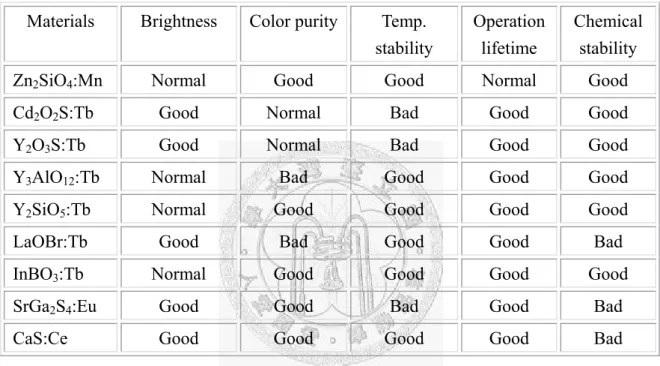
The main application for phosphors is for image displays. TV is the most common one. A CRT (cathode ray tube), in which phosphor coating on the screen, could be excited by accelerated electron beam, and emit light in the different colors. Red, green, and blue (RGB) are three basic optical elements that can create various colors visible to eyes. Red color can be generated by Y2O3:Eu. For green one, Cd2O2S:Tb and Y2SiO5:Tb are reported in literature. As for blue one, ZnS:Ag is the best. Several potential phosphors with Tm3+, Ce3+ and Eu2+ activators are still investigated [24]. Table 2- 2 lists several green phosphors and their properties. However, in the last 10 years of 20th century, CRTs displays become less common. In the contrary, flat panel displays (FPD) becomes popular with its advantages of low power consumption and light weight. FPD generally includes liquid crystal displays (LCD), plasma displays (PD), field emission displays (FED), and electroluminescent displays (ELD). Among those, the ELD shows the longest operation life time (more than 50,000h) with less luminescence decay [24].
Briefly speaking, luminescence properties could be divided into three categories:
photoluminescence (PL), electroluminescence (EL), and cathode luminescence (CL). As ceramic oxide based phosphors are concerned, there are two materials that we are interested in, host material and activator [25]. The host materials are usually insulators
Therefore, it could allow the inlet energy (e.g. UV light) exchanging by activators with limited energy loss. Aluminate (MAlO3), silicate (MSiO4), indiante (MInO3), galliante (MGa2O4) and phosphate (MPO4) are common ones that have been selected for host materials. As the activators, transition metals and rare earth elements are currently chosen due to their electron configuration with full or just half occupied orbital, e.g.
Mn2+, Tb3+, and Eu3+. Activators that doped in host materials induce substitutional defects if the ionic size and valence is not fully match. Thus a limitation of activators selection is concerned. The ion radius of substitutional ions and host cations should match one to each other. Otherwise, the lattice will suffer a residual stress. Table 2- 3 shows ionic radius of some cations with a coordination number (CN) of 4. All of the luminescence properties follow Stokes law or Stokes shifts, [26] which a higher energy (Ea) is adsorbed, and photons (hv) or heat (ΔH) are emitted or dissipated. Luminescence is described in more details as consisting of the following steps: (1) energy adsorption, (2) excitation of activators, as to form excited states, (3) relaxation of heat from excited states by lattice vibration, and/or (4) emission of lower energy photons, and relaxed to ground state.
The sources of activation energy able to create visible light emission include UV light (for PL), electric field or current (for EL), or accelerated electrons (for CL). For the case of PL, the electrons on their ground states adsorbed energy of. UV light, and
being excited to excited states, which correspond to un-occupied orbital existing in transition metals or rare earth elements. The band-gap between the states defines the emission wavelength of PL spectra.
For the case of EL, a typical thin film electroluminescence (TFEL) device was fabricated to a sandwich structure (or so called “M-I-S-I-M structure”), which composed of electrode, dielectric layers, phosphor layer, dielectric layers, and another electrode, as shown in Fig. 2- 7. Of course, at least one electrode must be transparent that the generated light is capable of emitting from the device. ITO (In-Sn-O) glass is the most common material that is used for one electrode. The other electrode is usually established by metal, especially aluminum which is cheap and able to fully reflect emitted light. Then, the insulators are coated or deposited on the electrode whatever by spin coating, vapor deposition methods or else.
In order to satisfy the activation mechanism of EL device, several properties for selection of capacitor are necessary, high dielectric constant, high electric field strength, and uniform thickness [27]. In the original state (i.e. no energy is applied), the insulators and phosphor layer act as three capacitors in series as Eq. 2.1:
p i
p i
i p p
i
C C
C C C
C C
C C C
C C
= +
∴
= + +
×
=
2
1 2 1 2
1
(eq. 2.1)
and phosphor layer, respectively. As the electric field increases, phosphor will break-down when a threshold voltage of the material is achieved. Thus, the equivalent circuit of the M-I-S-I-M structure could be seen in this circumstance as two capacitors in series (phosphor layer could be treated as a simple resistor). Therefore, the total capacitance could be expressed as eq. 2.2.
2 1 2 1
i i
C C C C
=
∴
×
=
(2.2)
Generally, if there is a material which generates light with an applied current, this light emission is so called as electroluminescence. Usually, in a semiconductor, a doped material with p-n junction has separated electrons and holes (and also can be generated by impact of energetic electrons accelerated by electric field). Electroluminescence is a result due to the recombination of electrons and holes and thus releases the energy as visible light [29]. There are four steps that describes the mechanism of EL: [28]
1. electrons tunnel from the insulator/phosphor interface 2. electrons are accelerated to be energetic
3. the energetic electrons impact-ionize the luminescent center or create electron-hole pairs that lead to the activation of the luminescent center
4. the luminescent center relaxes toward the ground state and emits visible light.
The required electric filed for operating an EL device at a frequency that high enough to
prevent from flicker for human eyes should be over than 60 Hz, and thus the applied field must be >2x10⁸ V/m [27]. This correspondent electric field created a voltage drop (a basic threshold voltage) across a phosphor layer of 500 nm could be easily calculated by Eq. 2.3, where V is voltage drop; E is applied electric field; and s is the thickness of
phosphor layer:
∫
⋅= E ds
V (2.3)
For the case of CL [30], the mechanism for CL is quite different form the above two. First, we will have an equipment to generate electrons with high velocity and voltage, such as CRT or field emission gun. In order to lower the threshold voltage, a vacuum environment is required. As the accelerated electrons strike samples, the surface creates electron-hole pairs. The separated p-n pairs will recombine together due to the attraction form Coulomb force at the p-n junctions [32]. Therefore, the electrons and holes encounter one another and continuously recombine if a reverse bias does not exist.
Energy releasing occurs and could be expressed as the following equation:
energy holes
eletrons+ → (2.4)
When the released energy is in visible spectrum, then we call this as cathode luminescence (CL). The released visible light could be observed by naked eyes. The photons could be also collected by PMT (photomultiplier tube) and transformed into
Table 2- 2 Green phosphors that have been used for optical instruments and their performance. [24]
Materials Brightness Color purity Temp.
stability
Operation lifetime
Chemical stability
Zn2SiO4:Mn Normal Good Good Normal Good
Cd2O2S:Tb Good Normal Bad Good Good
Y2O3S:Tb Good Normal Bad Good Good
Y3AlO12:Tb Normal Bad Good Good Good
Y2SiO5:Tb Normal Good Good Good Good
LaOBr:Tb Good Bad Good Good Bad
InBO3:Tb Normal Good Good Good Good
SrGa2S4:Eu Good Good Bad Good Bad
CaS:Ce Good Good Good Good Bad
Table 2- 3 Radii of some ionic species existed in crystals with CN = 4 [55]
Ion Radii (nm) Ion Radii (nm)
Ag+ 0.100 Hg2+ 0.096
Al3+ 0.039 In3+ 0.062
As5+ 0.034 Li+ 0.059
B3+ 0.011 Mg2+ 0.057
Be2+ 0.027 Mn2+ 0.083
C4+ 0.015 Mn4+ 0.039
Cd2+ 0.078 Na+ 0.099
Co2+ 0.058 Nb5+ 0.048
Cr4+ 0.041 Ni2+ 0.055
Cu+ 0.060 P5+ 0.017
Cu2+ 0.057 Pb2+ 0.098
Fe2+ 0.063 Sn4+ 0.055
Fe3+ 0.049 Ti4+ 0.042
Ga3+ 0.047 Zn2+ 0.074
Ge4+ 0.039
Fig. 2- 7 Structure of an EL device. The thickness of the phosphor layer in this case is about 700 nm. [31]
Fig. 2- 8 A schematic diagram showing EL mechanism in an EL device. [28]
2.3 Synthesis of Core-Shell Structures
Coating of colloidal particles with a layer of different material is used as a convenient way to modify the surface chemistry, reactivity, catalytic, optical, or magnetic properties of the particles. Such CS (core-shell) particles can be prepared either by controlled precipitation of inorganic precursors onto core particles or by other methods [33].
Colloidal particles with a low-index core and high-index shell, such as titania, are the suitable precursor for photonic crystals. The articles provided that the CS particles can be made monodispersive with a smooth coating [34]. Particles coated with titania are generally exceptionally difficult to synthesize because most of the titania precursors are highly reactive, making the steps difficult to control as precipitation [35]. Used titanium alkoxide in non-aqueous solvents as the precursors, only a monolayer of titania was deposited on copper, zinc oxide, silica, and gold nanoparticles by the hydrolysis of the alkoxide. The concentration of the reactants needed to be well controlled because high concentrations easily leaded to particle aggregation or formation of second titania particles.
Generally speaking, there are several ways to synthesis core-shell structure. For example, hydrothermal method, layer-by-layer method, osmotic swelling method, sol-gel method, and water/oil/water emulsion method are the most common techniques
reported in literature. These techniques are applicable to synthesize polymer core of polystyrene particles coated with titania, iron, silica-core alumina-shell, etc. [36-39].
2.3.1 Hydrothermal Method
The synthesis of submicron powders and thin films by hydrothermal method has been reported by Walton et al. [40], who indicated that there were two extremely models controlling the formation mechanism of t-BaTiO3. One was a homogenous solution phase reaction between titanium and barium hydroxyl anions by the dissolution- precipitation mechanism. The other is the reaction between solid titania and soluble barium salts (the in-situ heterogeneous transformation mechanism). The advantage of this method is appreciated to create the products at lower temperature. The products with good crystallization and uniform chemical composition can be obtained due to the homogeneous solution during the whole reaction.
2.3.2 Layer-by-layer Method
Layer-by-layer method is a kind of processing mechanism, by which the core and shell materials would be able to be attracted by each other. When these two materials
react with the solvent (for example, water) and become partial positively or partial negatively charging [41]. Therefore, base on the opposite charges, the coating material could coat on the core electro-statically. In addition, if the core is consisting of polymeric materials, then the core can be removed by calcination, or by dissolved in selected organic solvent to obtain a hollow sphere.
In Zhang’s study [42], they used PS, silica, and tetrabutyl titanate (TBT) to synthesize well-defined spherical silica-core PS-shell nanoparticles (SiO2-PS-CSNs).
The TBT was added into the sulfonated SiO2-PS-CSNs with ethanol and then hydrolyzed to allow TiO2 nano-particles coating on the surface, as the schematic diagram shown in Fig. 2- 9. The original size of SiO2-PS-CSNs is about 330 nm. After coating and calcination, the products experienced 29% shrinkage, and the TiO2 shell is 28 nm in thickness, as TEM micrographs shown in Fig. 2- 10. Besides, there is a silica layer which could be observed by TEM. Therefore, this method offered the possibility to construct double functional hollow spheres.
2.3.3 Osmotic Swelling
Osmotic swelling is starting from a nucleus on which coated with carboxylic function group. First, there is a hydrophobic monomer attached on the nucleus, when the base is added into the system, the core becomes a carbonate (R-COO-), then the part
with carbonate group will be pulled to the surface of the shell due to the solubility of the carbonate group in the water is much greater than a carboxylic acid (R-COOH) [43].
The hydrophobic shell will be pushed to the core. Finally, the core-shell structure becomes denser.
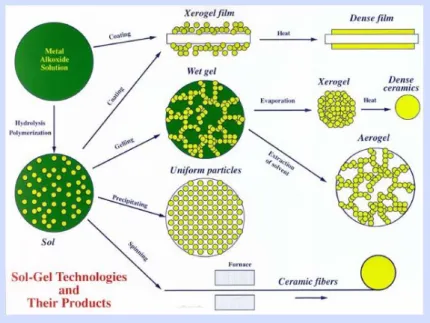
2.3.4 Sol-gel Method
In general, alkoxide is used as a precursor, which reacts with water, undergoing hydrolysis and condensation reaction. The Fig. 2- 11 illustrates a basic concept of sol-gel reaction that started from a metal alkoxide solution. If silica is synthesized as an instance, the mechanism could be described as follow: [44]
Hydrolysis:
Condensation:
Oxide materials made by sol-gel process have good performance on homogeneity, optical transparency, wearing resistance, and widely applied on various technical products.
In Wang’s study [38], they used α-alumina slurry and TEOS as starting materials.
The alumina slurry was diluted with ethanol to a suspension with 1~5% solid loading.
OH H C SiOH O
H H
SiOC2 5 + 2 ⇔≡ + 2 5
≡
O H SiOSi
SiOH
SiOH + ≡ ⇔≡ ≡ + 2
≡
OH H C SiOSi SiOH
H
SiOC2 5+≡ ⇔≡ ≡+ 2 5
≡
as reactor by adjusting the pH value to 11 at 50~75 .℃ Core-shell particles were collected after centrifuged and washed. In this case, the thickness of uniform silica layer coating on alumina particles was about 20 nm observed by TEM. No individual sol particles were found. The coating was a heterogeneous nucleation process. The SiO2
was surely bonded with the Al2O3 particles.
2.3.5 Water/oil/water (W/O/W) Emulsion
There are two phases in the beginning, water phase and oil phase. One surfactant was used to make latex. Then, another latex was added to obtain a w/o/w solution. After drying, the water phase in the center will disappear and a hollow particle presented, as shown in Fig. 2- 12.
In Kim’s study [45], the latex A consisted of SLS (sodium lauryl sulfate), Na(PO3)6, APG (Glucopen), water. The latex B contained MMA (methacrylate), EGDMA (ethylene glycol dimethacrylate), UA (urethane acrylate), Span 80 (sorbitan monooleate) and water. All ingredients of mixture A were dissolved in a container with a stirrer. The water-in-oil emulsion, which was prepared by sonification of mixture B, was dropped into the mixture A. Thus the w/o/w emulsion was prepared. Then, emulsion polymerization was carried out at 60 °C for 4 h. The precipitate was washed and dried. In this study, it was concluded that PMMA hollow particles can be prepared
by w/o/w emulsion polymerization. The increase in the viscosity and the hydrophilic of the monomer mixture caused by UA prevented the droplets coalescence during polymerization, and helped to form a multi-hollow particle.
SiO2-PS CSNs SiO2-PS-SPS CSNs HTNMSNs
Sulfonation TBT solution dissolution or calcination Fig. 2- 9 Schematic diagram indicating the processing steps to prepare hollow core-shell particles with layer-by-layer method. [42]
Fig. 2- 10 TEM micrographs showing the (a) (SiO2/PDADMAC)2-coated PS latex particles and hollow silica spheres after calcination with (b) one, (c) two and (d) three layers coating. [42]
Fig. 2- 11 Schematic diagram illustrating a sol-gel reaction resulting in the products of different morphologies. [46]
Fig. 2- 12 Schematic diagram representing the reaction steps of W/O/W emulsion. [45]
2.4 Synthesis of Zn2SiO4:Mn Material
Oxide phosphors have been practically used for fluorescent lamps, field emission displays, and plasma display panels. With the better chemical stability which leads to a longer operation life time and also the low toxicity compared to sulfate-based or polymer based phosphor materials (such as ZnS and organic-based LED), ceramic oxide phosphors materials are being more and more popular. The manganese doped zinc silicate is one of these materials that are going to be discussed.
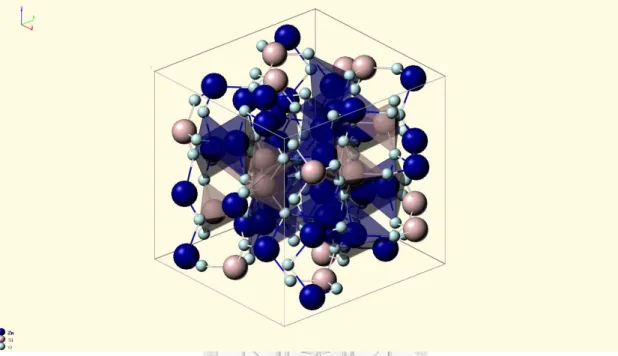
Zinc silicate, or the so called willemite, is a phosphor belonging to the rhombohedra structure with the density=4.221 g/cm3 [46], having the cell parameters of a=b=c=0.86280 nm and α=β=γ=107.87o and coordination number of 4 [47]. The crystalline structure of willemite was shown in Fig. 2- 13. It’s easy to see that each of Zn and Si ion bonding with 4 O2- ions and thus a tetrahedron is formed. Since the Mn and Zn ions have similar ionic radius (Mn2+=0.083 nm and Zn2+=0.074 nm) [55] and also the same coordination number of 4, Mn2+ ions are easily to diffuse into Zn2SiO4
system during heat treatment to substitute Zn2+ ion and then becomes a solid solution which could be marked as Zn1-XMnXSiO4 or Zn2SiO4:Mn. The Mn-doped zinc silicate has photoluminescence with the applied energy, for example, UV light, the 3d5 electron in Mn will be exited.
In the case of photoluminescence, an applied UV source is required. As everyone
knows, the Mn-doped zinc silicate has a 520-530 nm green light emission and could be observed by our naked eyes. Also, the electroluminescence property presents if there is an applied electric field as Fig. 2- 14.
There are several processes to synthesis Zn2SiO4:Mn. Solid state reaction, sol-gel, and hydrothermal method are the well known processes that were be applied commonly.
Most of them prepared Zn2SiO4:Mn in a thin film on various substrates, e.g. glass, silicon wafer, ITO (indium-tin oxide).
2.4.1 Zn2SiO4 Powders
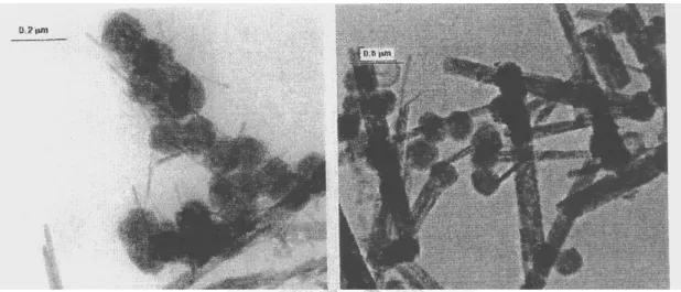
In 2000, Ahmadi et al. synthesis Zn2SiO4:Mn by hydrothermal method at low temperature (<250oC) without heat treatment to prevent formation of agglomeration and changing of valence state at elevated temperature [50]. (CH3O)4Si, water and ammonia were mixed and having a hydrolysis reaction for an hour in a container. And then, a designed ratio of manganese and zinc chloride were added into the container and placed into an autoclave with nitrogen has been bubbled in (to maintain the system in an inert atmosphere). The autoclave was heated to 250oC for 4 hours. The solution after the reaction was centrifuged and the supernatant was discarded. Finally the product was dried in an oven at 120oC and then being analyzed. The Zn2SiO4:Mn products were
Zn2SiO4:Mn made by this method. Two structures were found: the spherical one had an average diameter of 150 nm; the acicular particles had widths from 20-50 nm with the length range form 200-600 nm. The reason to the different particle shape may be resulted from the molar ratio of ammonia to zinc: if the ratio is lower than 1.7 then the spherical particles were formed; if the ratio is more than 4.9, then the acicular particles were presented.
Since the willemite is non-dissolvable in water, thus the Zn2SiO4:Mn powders could be dispersed in water with ultra sonic bath and with limited agglomerations. The suspension has a great polydispersity up to over than 25%, this phenomena was resulted form the two different morphologies (spherical and acicular shape) as which has been mentioned in the previous paragraph. The contribution of this research is the low temperature synthesis process. Crystallization formed as the reactants mixed in the autoclave at about 250oC instead of high temperature annealing and provided Zn2SiO4:Mn particles with green light emission under applied UV light.
A similar process was applied to synthesis the Zn2SiO4:Mn phosphor by sol-gel method. Thomas and his coworkers demonstrated their process in a basic solution, too [51], which included TEOS, Mn(CH3COO)2 and Zn(CH3COO)2 as precursors. The
“seeding” process was applied which completed by mixing those precursors to form a gel with ammonium polyacrylate (APA) and polyoxyethylene sornitan monooleate
(C12H10ClNO3). This seeding process leaded to a greater crystalline phase and a larger mean particle size (30=>180 nm).
A typical method for preparing Zn2SiO4:Mn is mixing both ZnO and SiO2 powders together and firing at elevated temperature with about 2% Mn-doping. The precursors for solid state reaction perhaps are: oxidized wafer or SiO2 powder for Si; ZnO, Zn(NO3)2 or Zn(CH3COO)2 for Zn2+; and Mn(NO3)2, Mn(CH3COO)2, Mn(CO3)2, or MnO for Mn2+ [49, 50, 56, 57]. Base on the phase diagram in Fig. 2- 16, it’s obvious to see that the pure zinc silicate phase formed at the molar ratio of Zn/Si=2:1. In fact, the homogeneity of powder mixing limits the purity of product. In other words, there should be either ZnO or SiO2 phases left after reaction unless the annealing temperature is high enough or even the whole system becomes in liquid state. Higher heat treatment temperature costs a lot.
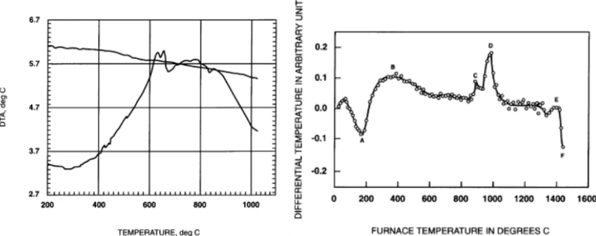
Adding flux into this system may be a good way to solve this problem. In Kitai’s study [31], ZnO, SiO2 and MnO were mixed with the addition of lithium fluoride (LiF).
The mixture was annealed at 800-850oC in argon atmosphere and then Zn2SiO4 was obtained. The reaction progress was examined by the differential thermal analysis (DTA). Fig. 2- 17 showed the results of two exothermic peaks: the first one may be the transition state, which indicated that an intermediate compound was formed at 630oC
the reaction of ZnO reacted with SiO2 and become Zn2SiO4 phase occurred at 650oC.
Compared to the sample without LiF, the result shows a stronger exothermic behavior, and the reaction occurred at the temperature approaching to 1000oC. So, the difference of flux adding or not was apparent.
Besides, adding flux into this system not only decreased the reaction temperature but also improved the brightness and efficiency on electroluminescence property. In Fig.
2- 18, the LiF was concerned. It’s easily to find that with the more flux doping, the brightness and efficiency raised up 33-50% at the 300 V applied voltage with frequency at 60 Hz. There are still some other flux that have been tried, including NaCl and K2SO4, which were also successfully reduced the reaction temperature on forming Zn2SiO4:Mn.
However, these materials did not be mentioned too much in Kitai’s study.
2.4.2 Zn2SiO4 Thin Film
Silicon-based opto-electric materials were also studied. The thin film zinc silicate was wildly used in optical application. Yun et al. [59] created phosphor thin film via chemical (precursors) solution depositing on ITO plates, and also, some other substrates were tried: Kitai [31] and Minami [60] constructed oxide phosphors EL devices like a sandwich structure (i.e. electrode/dielectric layer/phosphor layer/dielectric layer/electrode) with the dielectric layers composed of BaTiO3, SrTiO3 or else. The
thickness of the phosphor layer and dielectric layers ranged of 0.2-1 and several μm, respectively. Wafer is a common substrate that has been used in lots of researches.
Taghavinia [57] synthesized Zn2SiO4 on porous silicon layers. The solution that contains Zn and Mn salts was deposited on the silicon and then followed bt heat treatments. Ji [52] fabricated the zinc silicate thin film coated on oxidized silicon wafer by spin coating. Silicon wafer was set to be the substrate and being annealed at 1100oC to be oxidized into SiO2. This SiO2 layer was controlled to be less than 130 nm. The liquid solution contained Mn(CH3COO)2 and Zn(CH3COO)2 which dissolved in 2-methoxyethanol and a little bit of monoethanolamine (NH2CH2CH2OH). The reaction was completed at 60oC for 1 hr with stirring. Then, the solution was spin-coated on the surface of the substrate with the rotation speed of 5000 rpm. The film was dried and then annealed between 800-920oC for 4 hr in air. In this case, ZnO phase appeared first after 800oC annealing. With the increasing annealing temperature, the ZnO would react with silica substrate and thus transformed into zinc silicate (willemite) phase as Fig. 2- 19. For the samples processed at the temperature higher than 920oC, the willemite phase was presented instead of ZnO with the rhombohedral structure which could be identified by X-ray diffraction. The surface morphology was also observed by SFM (scanning force microscopy). The surface was covered with the densely coated
only 30.88 nm in the area of 2*2 μm2.
Fig. 2- 13 Crystal structure of willemite unit cell in this diagram represents the positions of Zn (dark balls), Si (light balls), and O (small balls) ions in this system. [53]
Fig. 2- 14 Two figures showing the PL and EL spectra, respectively. The PL and EL spectra of Zn2SiO4:Mn was coated as a thin film on wafer. [49]
Fig. 2.3-a Fig. 2.3-b
Fig. 2- 15 TEM images showing the Zn2SiO4:Mn made by Ahmadi’s method contains both the spherical and acicular shape. [50]
Fig. 2- 16 Phase diagram of ZnO-SiO2 system. [56]
Fig. 2- 17 DTA results of the ZnO-SiO2 mixture with LiF (left) and without LiF (right).
The reaction temperature was reduced by adding flux (LiF in this case) into the system.
[31]
Fig. 2- 18 Two EL spectra showing the emitting brightness and efficiency versus applied voltage of Zn2SiO4:Mn with adding LiF as a flux. [31]
Fig. 2- 19 X-ray diffraction analysis of the samples illustrating phase transformation temperature. The annealing temperatures varied with (a) 800oC, (b) 840oC, (c) 920oC and (d) 980oC [52].
Chapter 3 Experimental Procedure
3.1 Materials
The starting materials used in this study included TEOS (tetraethyl orthosilicate, 98 wt%, ACROS, USA), NH4OH (ammonium hydroxide, 28-30 wt%, ACROS, USA), C2H5OH (ethanol, 99.5% pure, SHIMAKYU, Japan), Zn(NO3)2 (zinc nitrate, which was prepared by dissolving ZnO powder in HNO3 solution; ZnO powder (億研堂, Lot:
0213012306, Taiwan); HNO3 solution (65 wt%, SHOWA, Japan), Mn(NO3)2 (98% pure, SHOWA, Japan).
3.2 Experimental Design
Fig. 3- 1 shows the flowchart of this study. The first part is to synthesize spherical silica particles in uniform size. These particles were used to react with Zn2+ and Mn2+
ion in order to form Zn2SiO4 shell on SiO2 particles. The products are fabricated in different morphologies, e.g. powders or photonic-bandgap (PBG) crystalline templates, which were assembled to form optical-electronic device. Therefore, various properties, photo-luminescence (PL), cathode-luminescence (CL), and microstructure were investigated to correlate the properties of loose particles and PBG with their core-shell
![Table 2- 1 A list showing the IEP point of some ceramic materials [16]](https://thumb-ap.123doks.com/thumbv2/9libinfo/9607742.633442/29.892.235.659.286.761/table-list-showing-iep-point-ceramic-materials.webp)
![Table 2- 3 Radii of some ionic species existed in crystals with CN = 4 [55]](https://thumb-ap.123doks.com/thumbv2/9libinfo/9607742.633442/37.892.221.672.339.867/table-radii-ionic-species-existed-crystals-cn.webp)
![Fig. 2- 8 A schematic diagram showing EL mechanism in an EL device. [28]](https://thumb-ap.123doks.com/thumbv2/9libinfo/9607742.633442/39.892.172.704.288.763/fig-schematic-diagram-showing-el-mechanism-el-device.webp)