國 立 交 通 大 學
電子工程學系 電子研究所碩士班
碩 士 論 文
相容於標準金氧半技術之光接收機前端電路
相容於標準金氧半技術之光接收機前端電路
相容於標準金氧半技術之光接收機前端電路
相容於標準金氧半技術之光接收機前端電路
Monolithically-Integrated Optical Receiver
Front-End in Standard CMOS Process
研 究 生 : 黃世豪
指導教授 : 陳巍仁
i
相容於標準金氧半技術之光接收機前端電路
相容於標準金氧半技術之光接收機前端電路
相容於標準金氧半技術之光接收機前端電路
相容於標準金氧半技術之光接收機前端電路
Monolithically-Integrated Optical Receiver
Front-End in Standard CMOS Process
研 究 生:黃世豪
Student : Shih-Hao Huang
指導教授:陳巍仁
Advisor : Wei-Zen Chen
國立交通大學
電子工程學系 電子研究所
碩士論文
A Thesis
Submitted to Department of Electronics Engineering and Institute of Electronics
College of Electrical and Computer Engineering
National Chiao-Tung University
in Partial Fulfillment of the Requirements
for the Degree of
Master
in
Electronics Engineering
September 2008
Hsin-Chu, Taiwan, Republic of China
ii
相容於標準金氧半技術之光接收機前端電路
相容於標準金氧半技術之光接收機前端電路
相容於標準金氧半技術之光接收機前端電路
相容於標準金氧半技術之光接收機前端電路
研 究 生: 黃世豪
指導教授:陳巍仁
國立交通大學
電子工程學系 電子研究所碩士班
摘要
摘要
摘要
摘要
本篇論文提出兩個相容於 0.18 微米標準金氧半技術之高速光接收機電路。這兩個光 接收機收到光訊號以後,可以將光訊號轉換成 800 毫伏特的電壓訊號來推動 50 歐姆的 輸出端負載。在第一項電路中,它將一個空間調變光感測器(Spatially Modulated Light)、一個轉阻 放大器和一個後級限伏放大器整合在單一晶片裡面。利用空間調變光感測器和適應性的 類比等化器(Equalizer)使本電路可以操作到每秒 31.25 億位元的資料速度。整顆晶片耗功 175 毫瓦。晶片面積是 0.7 平方毫米。 另外一項電路,它也整合了一個光感測器、一個轉阻放大器和一個後級限伏放大器 在單一晶片裡面。在不改變製程技術的情況下,我們提出一個新型的 PIN 光感測器。因 為有它,所以不需要等化器就可以操作到每秒 25 億位元的資料速度。整顆晶片耗功 138 毫瓦。晶片面積是 0.53 平方毫米。
iii
Monolithically-Integrated Optical Receiver Front-End
in Standard CMOS Process
Student: Shih-Hao Huang
Advisor: Wei-Zen Chen
Department of Electronics Engineering & Institute of Electronics
National Chiao-Tung University
Abstract
The thesis presents two solutions of the monolithically-integrated high-speed optical receivers in standard 0.18-µm CMOS technology. The optical receivers are capable of delivering 800 mVpp to 50 Ω output load after optical to electrical conversion.
For the first one, it integrates a spatially modulated light (SML) detector, a transimpedance amplifier (TIA), and a post limiting amplifier on a single chip. A 3.125 Gbps high speed operation is achieved by utilizing SML detector and adaptive analog equalizer (EQ). The total power dissipation is 175 mW, and the chip size is 0.7 mm2.
For the other, it also includes a photodetector, a TIA, and a post limiting amplifier on a single chip. A novel PIN detector is proposed and adopted in this design without technology modification. It can operate up to 2.5 Gbps without an equalizer. The total power dissipation is 138 mW, and the chip size is 0.53 mm2.
iv
Acknowledgment
經歷了 2005 年 7 月到 2008 年 9 月這交大碩士班兩年
兩年
兩年
兩年
時間,我終於拿到畢業證 書。這段時間真的多很多,以後不知道還不會多更多。我的意思是:在專業知識上多很 多,在處理事情的成熟度上也多很多。還好啦!之前的學長也是兩年
兩年
兩年
兩年
畢業。 感謝我的指導教授陳巍仁老師,在我專業知識上的指導。碩士班一起奮鬥”傻傻分 不清楚”的松諭和宗裕、”張巧玲瓏”的張巧玲、黃金 307 實驗室所有學長和學弟,感謝你 們給我這段時間快樂的回憶。也得感謝林森五少和新莊四少在大學和碩士期間所提供的 休閒娛樂。另外,必須感謝我的家人和 CI 現役的郁玲,不斷地對我付出和關懷,讓我 可以無後顧之憂完成碩士學位。最後,感謝我的觀世音菩薩,我畢業了! 黃世豪 08, Sep., 2008v
Contents
摘要
摘要
摘要
摘要 ...ii
Abstract ...iii
Acknowledgment ...iv
Contents ... v
List of Tables ...viii
List of Figures...ix
Chapter 1
Introduction ... 1
1.1
Motivation ... 2
1.2
Thesis Organization... 4
Chapter 2
All-Silicon Optical Receiver... 5
2.1
General Characteristics... 6
2.2
PN Junction Photodetectors... 10
2.2.1
Analysis of PN Junction Photodetectors ... 11
2.2.2
Simulation Results... 13
2.3
SML Detectors... 14
2.3.1
Basic Concepts ... 14
2.3.2
Analysis of SML detector... 15
2.3.3
Simulation Results... 16
2.4
Lateral PIN Detectors ... 17
2.4.1
Basic Concepts ... 17
2.4.2
Analysis of PIN detector ... 19
2.4.3
Simulation Results... 20
2.5
Fully CMOS Optical Receiver ... 21
vi
2.5.2
Specifications of Optical Receiver ... 22
Chapter 3
Transimpedance Amplifier... 26
3.1
Design Considerations... 27
3.2
Preamplifier Architecture ... 28
3.2.1
Architecture Comparison ... 28
3.2.2
Circuit Topology Comparison ... 30
3.3
Circuit Implementation... 33
3.4
Summary... 40
Chapter 4
Limiting Amplifier... 42
4.1
Design Considerations... 42
4.2
Limiting Amplifier Architecture... 44
4.2.1
Architecture Comparison ... 44
4.2.2
Analysis of Stage Number... 45
4.3
Limiting Amplifier Implementation ... 47
4.3.1
DC Offset Cancellation Network ... 48
4.3.2
Gain Cell Design ... 49
4.4
Summary... 53
Chapter 5
Adaptive Equalizer and Buffer ... 55
5.1
Equalizer Circuit... 55
5.2
Output Buffer... 60
5.2.1
Output Buffer Implementation ... 61
5.2.2
Output Buffer Comparison ... 63
Chapter 6
Optical Receiver Realizations ... 65
6.1
A 3.125 Gbps AFE with SML Detector... 66
6.1.1
SML Detector ... 66
6.1.2
Architecture ... 67
6.1.3
Test Chip... 68
6.1.4
Measurement Results ... 70
6.2
A 2.5 Gbps AFE with PIN Detector ... 74
6.2.1
PIN Detector... 74
6.2.2
Architecture ... 74
6.2.3
System Simulation Results... 75
6.2.4
Test Chip... 77
6.2.5
Measurement Results ... 79
6.3
Performance Benchmark ... 83
vii
Appendix A PCB Layout ... 86
References... 88
Vita ... 90
viii
List of Tables
Table 2-1 Bandgap energy and threshold wavelength for PD materials. ... 6
Table 2-2 Comparison of the PN junction PDs with reverse-bias 1.2 V... 13
Table 2-3 The specifications of the OEIC with SML detector. ... 25
Table 3-1 Comparison of three topologies of preamplifier... 30
Table 3-2 Comparison of three preamplifiers... 32
Table 3-3 Post-layout simulated results (RCC) of TIA. ... 41
Table 4-1 Post-layout simulated results (RCC) of limiting amplifier... 54
Table 5-1 Buffer’s performance comparison with the same DC gain. ... 64
Table 5-2 Buffer’s performance comparison with the same output swing. ... 64
Table 6-1 The pad descriptions of OEIC with SML detector. ... 69
Table 6-2 The pad descriptions of OEIC with PIN detector... 78
Table 6-3 Performance benchmark... 82
ix
List of Figures
Figure 1-1 Simplified optical pickup organization. ... 3
Figure 1-2 The scenario of tera-scale computing... 3
Figure 2-1 Absorption coefficient of several photodiode materials versus wavelength. .... 7
Figure 2-2 The reflectivity with and without passivation in standard CMOS process. ... 8
Figure 2-3 Responsivities of photodetectors as a function of wavelength... 9
Figure 2-4 PN diodes in the generic CMOS technology... 10
Figure 2-5 Cross section of a single PN junction PD. ... 11
Figure 2-6 (a) top view, and (b) cross view of a SML detector... 14
Figure 2-7 Frequency response of a SML detector’s photocurrent... 15
Figure 2-8 SML detector simulated results. ... 17
Figure 2-9 (a) top view, and (b) cross view of a PIN detector. ... 18
Figure 2-10 Frequency response of a PIN detector’s photocurrent. ... 18
Figure 2-11 Simulated results of a PIN PD... 21
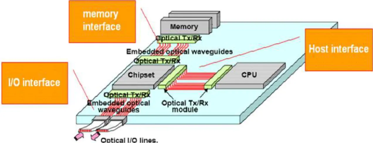
Figure 2-12 High density optical link for next generation CPU... 22
Figure 2-13 Optical transceiver architecture... 22
Figure 3-1 (a) low-impedance, (b) high-impedance and (c) transimpedance preamplifier architecture... 29
Figure 3-2 Architecture of common source feedback amplifier. ... 31
Figure 3-3 Architecture of common-gate feedback amplifier... 32
Figure 3-4 Fully transimpedance amplifier with SML detector. ... 34
Figure 3-5 Equivalent half circuit of TIA in Figure 3-4... 35
Figure 3-6 (a) Step response and (b) frequency response for damping factor. ... 35
Figure 3-7 The equivalent half circuit with noise source... 38
Figure 3-8 Magnitude response of TIA with SML detector. ... 39
Figure 3-9 Group delay of TIA with SML detector. ... 39
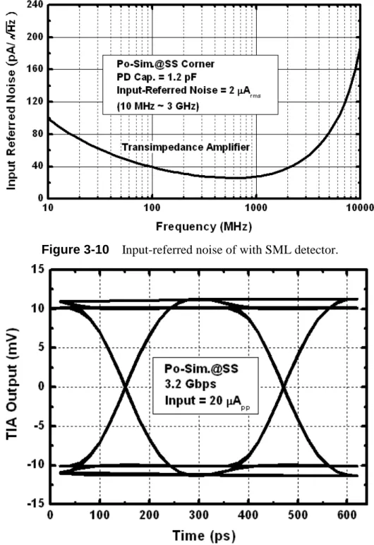
Figure 3-10 Input-referred noise of with SML detector... 40
Figure 3-11 Eye diagram for 3.2 Gbps and 0.02 mApp input current... 40
x
Figure 4-2 Limiting amplifier output with and without offset voltage. ... 44
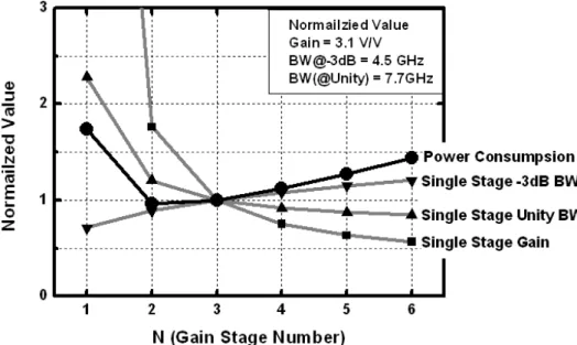
Figure 4-3 Normalized LA’s power consumption versus the number of stages. ... 47
Figure 4-4 Limiting amplifier is composed of SUB and 5 gain cells. ... 47
Figure 4-5 Feedback type limiting amplifier architecture... 48
Figure 4-6 Gain cell in the limiting amplifier. ... 49
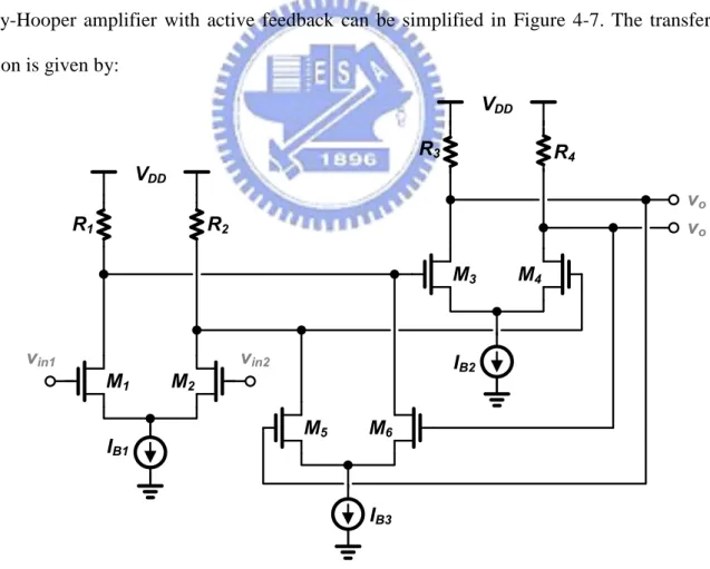
Figure 4-7 Active feedback architecture. ... 50
Figure 4-8 Subtractor schematic in the limiting amplifier. ... 51
Figure 4-9 Magnitude responses of subtractor, gain cell and slicer. ... 52
Figure 4-10 Magnitude responses of LA and front 3 stage... 52
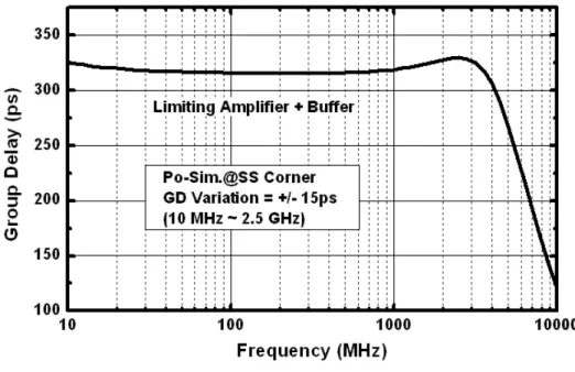
Figure 4-11 Group delay of LA. ... 53
Figure 4-12 Input-referred noise of LA. ... 53
Figure 4-13 Simulated eye diagram of LA. ... 54
Figure 5-1 (a) Capacitance/resistance degeneration, (b) frequency response... 56
Figure 5-2 The equalizer circuit... 56
Figure 5-3 Adaptive equalizer... 57
Figure 5-4 Transient simulation of the slope detector... 58
Figure 5-5 Two stage error amplifier. ... 59
Figure 5-6 Connection of this OEIC and an oscilloscope through a transmission line. ... 60
Figure 5-7 Open-drain output buffer. ... 61
Figure 5-8 Open-drain output buffer. ... 62
Figure 5-9 A simple differential stage... 62
Figure 5-10 FT-doubler output buffer... 63
Figure 6-1 Measured magnitude response of SML detector. ... 66
Figure 6-2 Optical receiver front-end architecture... 67
Figure 6-3 Chip layout of OEIC with SML detector... 68
Figure 6-4 Measurement setup... 70
Figure 6-5 Chip micrograph of OEIC with SML detector. ... 71
Figure 6-6 Measured bit error rate performance of the OEIC. ... 71
Figure 6-7 Eye diagram at 2.5 Gbps with the maximum input power, -3 dBm. ... 72
Figure 6-8 Eye diagram at 2.5 Gbps with sensitivity level, -5.8 dBm... 72
Figure 6-9 Eye diagram at 3.125 Gbps with the maximum input power, -3 dBm. ... 73
Figure 6-10 Eye diagram at 3.125 Gbps with sensitivity level, -4.2 dBm... 73
Figure 6-11 Optical receiver architecture ... 74
Figure 6-12 Magnitude responses of OEIC with PIN detector. ... 75
Figure 6-13 Group delay of OEIC with PIN detector. ... 76
Figure 6-14 Input-referred noise of OEIC with PIN detector. ... 76
Figure 6-15 Post-Simulated eye diagram for OEIC with PIN detector. ... 77
xi
Figure 6-17 Chip micrograph. ... 79
Figure 6-18 Measured BER performance @2V PD reversed-bias. ... 80
Figure 6-19 Measured BER performance @6V PD reversed-bias. ... 80
Figure 6-20 Eye diagrams at 1.25 Gbps with sensitivity level, -10 dBm. ... 81
Figure 6-21 Eye diagrams at 2.5 Gbps with sensitivity level, -7 dBm. ... 81
Figure A-1 Top layer of the PCB layout composed of 4 layers with RF-4. ... 86
Figure A-2 The PCB photograph measured 60 mm x 42 mm. ... 87
1
Chapter 1
Introduction
The growing demand on broadband Internet access has motivated development of low-cost, high-sensitivity optical receivers with high-speed operation. Optical receiver with monolithically-integrated photodetector has drawn tremendous research efforts recently. In contrast to conventional multi-die solutions, which composed of photodetector implemented in more expensive GaAs or InP-InGaAs technology, the fully integrated optical receiver is much more cost effective. Besides, the issues of parasitic capacitance introduced by ESD pads and leading inductance for multi-die integration can be avoided.
The fully-integrated optical receiver front-ends presented in this thesis are designed in standard 0.18 µm digital CMOS technology. The reason for choosing deep-sub-micron CMOS technology is the possibility to easily integrate a signal-processing part. The signal does not leave the chip after the optics received by photodetector in the receiver front-end. Therefore, output driver and output impedance matching are saved in system-on-a-chip (SoC).
2
1.1 Motivation
Over the past several decades, complementary metal oxide silicon (CMOS) technologies have the advantage that they are developed much more rapidly on the market than the other technologies, such as bipolar and BiCMOS. Thus, bipolar and BiCMOS technologies are more expensive than CMOS process of the same structure size.
Besides, the optical communication systems operate at wavelengths near 850 nm is of interest due to the wide availability of laser sources. Therefore it is obviously that CMOS is suitable for optical interconnection owing to the advantages of high-density and low-cost. They can be used in short distance and high volume communication systems, such as optical storage system, local area network and back plane interconnect.
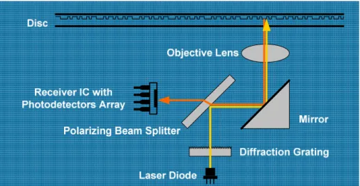
Optical Pickup Unit
Data on an optical disc is physically contained in pits which are precisely arranged on a spiral track. Figure 1-1 illustrates the light beam generated by the laser diode, passing through a diffraction grating, directed by polarization beam splitter and mirror. Finally, the light passes through the objective lens. When a light beam strikes a land interval between two pits, the light is almost totally reflected. On the other hand, when it strikes a pit, destructive interference occurs and a lower light intensity is returned.
The reflected light passes through the objective lens, then directed by mirror and polarization beam splitter. Finally, it will project onto the photodetectors array in receiver IC. If higher light intensity is received, then photodetector generates larger photocurrent, and vice versa. Thus, data one or data zero can be interpreted.
The use of blue laser provides a dramatic increase in storage capacity. Therefore, monolithically-integrated optical receivers with high-speed operation are suitable for the next-generation optical stage systems.
3
Figure 1-1 Simplified optical pickup organization.
Figure 1-2 The scenario of tera-scale computing.
Tera-Scale Computing
Figure 1-2 illustrates a scenario of tera-scale computing projected by Intel. A multi-cores platform has become a main stream to realize an energy efficient computing system in the future. Meanwhile, more and more channel bandwidth are demanded to sustain the heavy data traffic between the multi-cores in the enormous computing system. In such a data intensive platform, high density electrical interconnects may suffer from severe cross talk and electro-magnetic interference. On the contrary, optical link can alleviate these difficulties in system integration while they provide more data bandwidth.
4
In order to achieve this data rate of tera-bit per second, it is a nice solution by using multi-channel optical communication owing to its less crosstalk and EMI effect. In addition, small form factor and low cost optical transceiver could be the enabling technologies to fulfill the bandwidth requirement and realize the tera-scale computing platform.
1.2 Thesis Organization
This thesis consists of seven chapters. The first one is the introductory chapter where motivation is given. The goal is to design a monolithically optical receiver in standard CMOS process, and bit-rates up to a fewer Gbps. This achievement can minimize the total cost of the optical system.
Chapter 2 describes the CMOS photodetectors including PN junction photodetectors, spatially modulated light detectors and a novel PIN detector. Also, the specifications and challenges of the all-silicon optical receiver are discussed in this chapter.
Chapter 3 introduces trans-impedance amplifier (TIA). First, I will point out the design issues. Then the pre-amplifiers and TIA topologies will be described and compared. Besides, the noise analysis and circuit implementation be introduced one by one. At last, simulation results will be showed.
Chapter 4 introduces limiting amplifier (LA). Architecture will be described first. Then, stage number decision is analyzed. Offset cancellation, Cherry-Hooper circuit. At last, the LA’s simulated results will be showed.
Chapter 5 introduces the adaptive equalizer and output buffer.
Chapter 6 introduces the two OEICs which are realized by using the 0.18-µm standard CMOS technology. The measured results will also be showed in this chapter.
5
Chapter 2
All-Silicon Optical Receiver
Typically, the speed enhancement techniques of the photodetector can be classified into two categories. One approach is to get rid of the slowly diffusive carriers to achieve a high speed operation [1]-[5], and the other approach is to compensate the frequency response of the photodetector by utilizing equalizer [6]. From technology aspect, the former approach can be achieved by using a buried oxide layer [4] or SOI [5] process, but it requires nonstandard CMOS technology and additional cost. An alternative approach is by employing spatial modulated light (SML) detector [1]-[2].
In this chapter, we will first discuss the PD’s related general characteristics. Following section 2.1, the conventional PN junction photodetectors will be introduced in section 2.2. Owing to the shortcomings, such as low bandwidth and low responsivity, of PN junction photodetectors, then the high-speed spatially-modulated light (SML) detector is described in section 2.3. And section 2.4.introduces a novel lateral PIN. At last, the fully CMOS optical architecture will be introduced and system specifications will be listed.
6
2.1 General Characteristics
To design a CMOS photodetectors, what to do first is to understand the silicon characteristics. This section introduces the basics such as threshold wavelength, absorption coefficient, reflectivity, quantum efficiency and responsivity.
Threshold Wavelength (
λλλλ
g)
The energy of a photo is E = hν where h is the Plank’s constant, about 6.625 10× −34 J-s or
15
4.135 10× − eV-s, and ν is the frequency of the photo. It is given by
( )
1.24 c hc m E Eλ
µ
ν
= = = (2-1)where E is the photo energy in eV and c is the speed of light, about 3 10× 8 m/s.
The creation of electron-hole pairs requires the photon energy to be at least equal to the bandgap energy Eg of the semiconductor material to excite an electron form the valance band
to the conduction band. The threshold wavelength (or the upper cut-off wavelength)
λ
g istherefore determined by Eg or,
( )
1.24 g g m E λ = µ (2-2)Table 2-1 [7] lists some typical bandgap energies and the corresponding threshold wavelengths of various photodiode semiconductor materials. It is clear that Si photodiodes cannot be used in optical communications at 1.31 µm and 1.55 µm.
Table 2-1 Bandgap energy and threshold wavelength for PD materials.
Materials Eg (eV) @ 300K
λλλλ
g (µm) @ 300K GaAs 1.43 0.87 InP 1.35 0.91 Si 1.12 1.11 In0.53Ga0.47As 0.75 1.65 Ge 0.66 1.877
Absorption Coefficient (
α
)
Incident photos with wavelength shorter than
λ
g become absorbed as they travel in thesemiconductor and the light density, which is proportional to the number of photos, decays exponentially with distance into the semiconductor. The light intensity P at a distance x from
the semiconductor surface is given by
( )
o exp(
)
P x = ⋅P −
α
x (2-3) where Po is the intensity of the incident radiation and α is the absorption coefficient thatdepends on the photo energy or wavelength
λ
. Absorption coefficient α is a material property.For example, for Si, α can be approximated with the following formula [8]:
2 3
10
log
α
=13.2131 36.7985−λ
+48.1893λ
−22.5562λ
(2-4)where
λ
. is the wavelength of the input light signal.λ
. is given in µm whereas α is given incm-1. Most of the photo absorption (63%) occurs over a distance 1/α and 1/α is called the penetration length δ. For Si, α = 793.65 cm-1 and δ = 12.6 µm.
Figure 2-1 [7] shows α versus
λ
characteristic of various semiconductors where it is apparent that the behavior of α with the wavelengthλ
depends on the semiconductor material.8
Reflectivity (r)
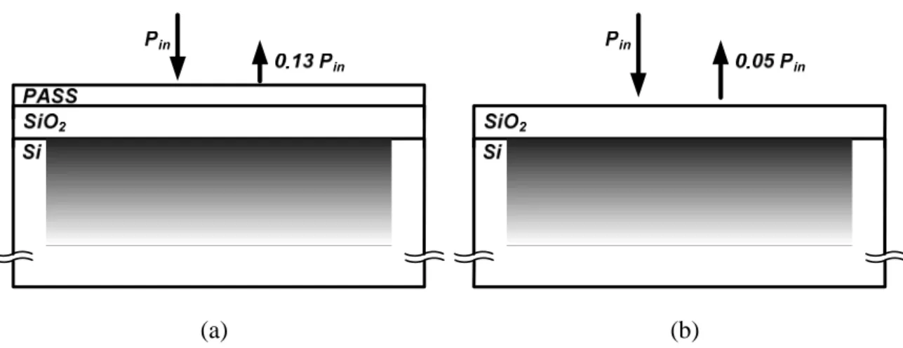
A fraction of incident optical power is reflected due to the difference in the index of refraction between the surroundings nο (air: 1.0) and the semiconductor nsi (Si: 3.5). For a
standard CMOS technology, the dielectric layers above the active region of photodetector comprise inter-layer dielectric, inter-metal dielectric (SiO2: nso ~ 1.45), and optional
passivation layers (Si3N4: nsn ~ 2.0), Using the impedance-transformation approach [9], the
effective impedance, Z, and the reflectivity, r, of the photodiode can be expressed as:
2 0 0 cos( ) sin( ) cos( ) sin( ) Si D D D Si n kd i n kd Z n n kd i n kd Z r Z
η
η
+ ⋅ = + ⋅ − = + (2-5) (2-6)where nD,nsi, and no denotes the intrinsic impedance of the dielectric layers, silicon substrate,
and air, respectively; k and d indicates the wavenumber and thickness of the dielectric layers,
respectively. With 850-nm light, the simulation results reveal that the reflectivity is around 0.13 and 0.05 for the device with and without passivation layer, respectively. Therefore, the reflectivity can be improved by removing the passivation layer above the active region of the photodetectors. Figure 2-2 illustrates that the reflectivity with passivation layer is 2.6 times less than that with passivation layer in standard 0.18-µm CMOS process technology.
(a) (b)
9
Quantum Efficiency (
ηηηη
)
The quantum efficiency is defined as the average number of generated electron-hole pairs per incident photo. In the shallow CMOS technology, the optical light penetrates deeper into ilicon and some of the photogenerated carriers will be recombined and reduce the quantum efficiency. Typically, the value of quantum efficiency in a CMOS is about 40 % to 70 %.
Responsivity (R)
For the development of optical receiver circuits, it is interesting to know how large the photocurrent is for a specific power of the incident light with a certain wavelength. The responsivity R is a useful quantity for such a purpose:
( )
1.243 o o PD opt q I A R W P hcλ
η
λ η
= = = (2-7)where
λ
o is in µm. The responsivity is defined as the photocurrent IPD divided by the incidentoptical power Popt. R depends on the wavelength, therefore the wavelength has to be
mentioned if a responsivity value is given.
The dashed line in Figure 2-3 [7] represents the maximum responsivity of an ideal photodetector with h = 1 % or 100 %. Unfortunately, the quantum efficiency is reduced by the partial recombination of photogenerated carriers.
10
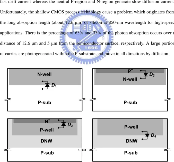
2.2 PN Junction Photodetectors
The simplest way to build integrated photodetectors is to use the PN junctions available in standard CMOS technology. Figure 2-4 shows the typical PN diodes in the triple-well (including N-well, P-well and deep N-well (or DNW)) CMOS process technology. The PN junctions of D1, D2, D3 and D4 are N-well/P-substrate, P+/N-well, N+/P-well and P-well/DNW,
respectively. The depletion regions of the PN photodetectors are shallow because they are less than 5 µm deep from the semiconductor surface.
When a photodetector is illuminated with an adequate light, its depletion region generates fast drift current whereas the neutral P-region and N-region generate slow diffusion current. Unfortunately, the shallow CMOS process technology cause a problem which originates from the long absorption length (about 12.6 µm) of silicon at 850-nm wavelength for high-speed applications. There is the percentage of 63% and 33% of the photon absorption occurs over a distance of 12.6 µm and 5 µm from the semiconductor surface, respectively. A large portion of carries are photogenerated within the P-substrate and move in all directions by diffusion.
P-sub N-well P+ D2 D1 N-well P-sub P-sub N+ D3 P-well P-sub P-well DNW DNW D4
11
Thus, for photodetector D1, most of the photocurrent is the slow diffusion current which is
generated by the P-substrate, thus the high -3 dB bandwidth of D1 is quite low. Although D2
and D3 have higher bandwidth because of isolating the slow P-substrate diffusion current by
N-wll or depp N-well, the shallow and narrow depletion region result in small responsivity. Compared to D2, D4 delivers larger responsivity. Unfortunately, D2, D3 and D3 exhibit large
parasitic capacitance owing to their high doping concentration. Thus, it is not easy to design a high-speed and high-responsivity PD under the un-modified digital CMOS technology.
2.2.1 Analysis of PN Junction Photodetectors
For the un-shaded area, the incident photon flux density is given by:
( )
opt( ) ( )
1-o P t t r A hcλ
Φ = (2-8)where Popt(s) is the input optical power, A is the device area,
λ
is the wavelength of theincident light, h is the Plank’s constant, c is the speed of light, and r is the reflectivity.
Consider a single PN junction photodetector structure shown in Figure 2-5. The generation rates of carriers per unit volume is
( )
( )
-o
, x
g x t = Φ
α
t eα (2-9)12
N
-
Type Neutral RegionIn the N-type neutral region, the continuity equation for holes in the time-domain is
( )
( )
( )
( )
τ ∂ ∂ = + ∂ ∂ 2 2 , , , - , n n n p p p x t p x t p x t D g x t t x (2-10)where Dp is hole diffusion coefficient and
τ
p is hole diffusion time in N-type neutral region.The boundary conditions are
0 1 0 0 n x n x L p x p = = ∂ = ∂ = (2-11) (2-12) If the concentration of hole-carriers is given, then the responsivity and frequency response of the diffusion current from N-type neutral region is got. In order to solve this problem analytically, the Laplace transform in the frequency domain is taken, and the Fourier series in the space domain is used [8]. Then the hole-carriers diffusion current can be solved as:
( )
(
) ( )
(
)
(
)
(
) ( )
( )
(
)
1 m+1 - L m+1 1 2 1 2 1 1 2 P 1 2 1 1 e +2 L 2 1 1 2L 2 1 L + 2 2 1 1 s+D + 2L p p m o p m m I s AqD m s m απ
α
π
α
π
α
π
τ
∞ = − − − = − − Φ × − ∑
(2-13)P
-
Type Neutral RegionIn the P-type neutral region, the continuity equation for electrons in the time-domain is
( )
2( )
( )
( )
2 ', ', ', - ', ' p p p n n n x t n x t n x t D g x t t x τ ∂ ∂ = + ∂ ∂ (2-14)where Dn is electron diffusion coefficient,
τ
n is electron diffusion time in P-type neutral regionand x’ = x – (L1 + D1). The boundary conditions are
' 0 ' 2
0
'
0
p x p x Ln
x
n
= =∂
=
∂
=
(2-15) (2-16)13
Then the electron-carriers diffusion current in the P-type neutral region can be obtained as:
( )
( )( )
(
) ( )
( )
2 1 1 -2 2 2 1 2 2 12
1-
1
2
1
2
m L L D o n n m n nm
e
m
s
I
s
AqD
e
L
L
m
m
s
D
L
α απ
π
α
α
π
π
τ
∞ + =
−
Φ
=
×
+
+
+
∑
(2-17) Depletion RegionIn the depletion region, the fast drift current is
( )
( )
- L1 - - (L1 D1)dr o
I s = AqΦ s eα eα + (2-18) Thus, the photocurrent of conventional PN junction photodetector can be expressed as
( )
( )
( )
ph p n dr
I = I s +I s +I s (2-19)
2.2.2 Simulation Results
Table 2-2 lists the simulated results of the PN junction PDs with reverse-biased voltage of 1.2 V. The conventional PN junction photodetectors have many disadvantages, such as low speed in N-well/P-substrate PD, small responsivity in P+diff/N-well, N+diff/P-well PD, and large parasitic capacitance in DNW/P-well, P+diff/N-well, N+diff/P-well PD. Thus, these CMOS photodetectors are not suitable for the general optical receiver to integrate directly without an equalizer or some good-performance front-end circuit.
Table 2-2 Comparison of the PN junction PDs with reverse-bias 1.2 V.
Diode Type -3dB Responsivity
(mA/W) -3dB Bandwidth (GHz) Cap. per 652
µµµµ
m2 (fF) N-well/P-sub 379.1 0.001 473 P+/N-well 30 1.3 3284 N+/P-well 29.9 1.9 2983 P-well/DNW 49 1.2 205114
2.3 SML Detectors
From the perspective of a high speed light detection, the impacts coming from the slowly-diffusive current should be circumvented. In addition, to keep the wide depletion region and low parasitic capacitance, the lightly doing P-substrate and N-well will be adopted. Thus, an alternative approach is by employing spatially modulated light (SML) detector.
2.3.1 Basic Concepts
As shown in Figure 2-6, a SML detector consists of a row of photodetectors alternatively covered and uncovered with light blocking materials, such as metal layers. The covered detector is named dark detector, while the uncovered detector is named illuminated detector. As the slow carriers generated in the neutral regions of the photo detectors diffuse in all directions, they can be partially eliminated by subtracting the photo current collected by the dark detectors (mainly composed of slow carriers) from that of the illuminated detector (composed of both fast-drifting and slowly-diffusing carriers). So, the SML detector is capable of high-speed operation.
15 ida rk (d a rk c u rr e n t) i il lu . -ida rk iillu . (i ll u . c u rr e n t)
Figure 2-7 Frequency response of a SML detector’s photocurrent.
The photocurrent component of a SML detector is shown in Figure 2-7. The illuminated current (iillu.) collected by illuminated detectors consists of the fast drift current from depletion
region, the slow hole-carriers diffusion current from N-well neutral region, and slow electron-carriers diffusion current from the P-substrate. On the other hand, the dark current (idark.) collected by illuminated detectors only consists of the slow electron-carriers diffusion
current from the P-substrate. If the slow electron-carriers diffusion current generated by the P-substrate diffuse the same amount (Ix) of current to the illuminated and un-illuminated
detectors at the same time, then most of the slow diffusion current can be removed (iillu. - idark)
by utilizing a differential TIA followed by a SML detector.
2.3.2 Analysis of SML detector
The photocurrent of the proposed SML detector can be expressed as:
ph illu dark p nI nD dr
I = I −I = I +I −I +I (2-20)
where Ip is the hole diffusion current in the N-well neutral regions, InI and InD are the electron
diffusion current in the P-substrate neutral regions of the illuminated detectors and the dark detectors, respectively, and Idr is the drift current in the depletion regions.
16
(
) ( )
( )
(
)
(
) (
)
(
)
(
)
(
)
( )
(
)
(
)(
)
1 1 1 2 1 1 1 2 1 1 2 2 2 1 1 1 2 1 1 2 4 4 2 2 1 2 1 2 1 2 1 1 2 1 2 1 2 1 1 2 2 2 2 1 2 1 2 1 m L o p p m n k YP ZP m p p p p Y Z Y Z Aq D m e L I L L m n k L m n k j f D D D L L L m L L L L L n k α α π α π π π α π π π π τ π + − ∞ ∞ ∞ = = = + Φ − − + = × × × − − − + × × − − − − + + + + ′ ′ ′ ′ − × + − −∑∑∑
(
)
(
2 8 21 2)(
1 1)
1(
2 8 2(
1 2)(
1)
1)
Z Y Y Z n L L k m k m n L π L π ′ − ′ − + − − − − ′ ′ (2-21)where α is the absorption coefficient, Φo is the incident photon flux density, and Dp and τp is diffusion constant and lifetime for holes, respectively. The frequency response is mainly determined by the term which involves f. It reveals that the bandwidth is proportional to the
sub-term:
(
)
2(
)
2(
)
2 1 2 1 2 1 2 1 1 2 p p p p Y Z m n k D D D L L Lπ
π
π
τ
− − − + + + ′ ′ (2-22)Since Dp, L1, and τp are restricted by a standard technology, the bandwidth can be improved by adopting shorter lengths (LY and LZ) of the rectangular shape to get smaller LY’ and LZ’. In
a similar way, the electron diffusion current of the P-well neutral region can be obtained. Furthermore, the drift current, proportional to the area of the depletion region Adr, is given
by [7]:
x dr dr o
I =
∫
A qα
Φ e−α dx (2-23)2.3.3 Simulation Results
Based on physical parameters of a standard 0.18-µm CMOS technology, the simulated results of photocurrent as functions of operating frequency is shown in Figure 2-8. The calculated responsivity of strip-line detector is about 62 mA/W, while its -3 dB bandwidth is about 2.1 GHz. In spite of the smaller responsivity, the responsivity bandwidth product (RBW) is much better than the conventional N-well/P-substrate junction photodetector.
17
Figure 2-8 SML detector simulated results.
2.4 Lateral PIN Detectors
To circumvent the mentioned issues of conventional N-well/P-substrate SML detector without resort to a sophisticated equalizer, we proposes a novel lateral PIN detector, emulated by a P+diffusion/P-well/N+diffusion interleaved architecture.
2.4.1 Basic Concepts
Figure 2-9 illustrates the top view and cross-sectional view of the detector. The detector is fabricated in the active region, surrounded by N-well and deep N-well (DNW). The top of the sensing region is striped of salicide and passivation layer to disconnect P+/P-/N+ regions and alleviate light reflection. Compared to conventional N-well/P-substrate junction, the electron-hole pairs are mainly generated in the laterally depleted regions. On the other hand, the well is tied to the highest voltage, which protects the PIN diode from substrate noise coupling.
18
Figure 2-9 (a) top view, and (b) cross view of a PIN detector.
iph 1 iph 2 iph 3
Figure 2-10 Frequency response of a PIN detector’s photocurrent.
Besides, there are still wide depletion region between P-well and DNW (or N-well), since the doping of these two neutral regions is not as heavy as that of P+diffusion or N+diffusion. Thus, the fast drift current generated by P-well/DNW (or P-well/N-well) depletion can also be collected to increase the responsivity of this PIN detector.
The photocurrent component of a PIN detector is shown in Figure 2-10. The photocurrent (iph1) of P-substrate/N-well junction PD exhibits a large diffusion current generated by
P-substrate so that its bandwidth is low. By employing the DNW and N-well, this PIN detector gets rid off the slow diffusion current. Thus, the percentage of fast drift current of the
19
total PIN’s photocurrent (iph2) increases. In addition, if a higher reverse-biased voltage is
applied, then Idrift becomes more and Idiff goes less owing to the fully-depleted P-well region.
Therefore, the high-speed PD with photocurrent iph3 is achieved.
2.4.2 Analysis of PIN detector
To comply with the diameter of the multi-mode fiber, the dimension of the photodetector is only 50 µm × 50 µm (A), consisting of 13 P-I-N fingers (see Figure 2-9). In this experimental
prototype, the P+ and N+ stripes are 1.45-µm wide (w), separated by a 0.5-µm wide P-well
region (d). Thus a reasonable low (~ 2 to 6 V) reverse biased voltage (VR) is sufficient to
deplete the P-well region of the photodetector for a high speed operation. The proposed architecture is expected to provide a higher responsivity by enlarging the P- region and operated in the avalanche mode. In this case, a higher reverse-biased voltage can be applied. The photocurrent of the proposed PIN detector can be expressed as:
ph p n dr
I = I + +I I (2-24) where Ip and In are the hole and electron diffusion current of the neutral regions, respectively,
and Idr is the drift current of the depletion regions.
Also, the hole-carrier diffusion current can be solved as [8]:
(
)
(
)
(
)
(
) ( )
( )
(
)
(
) ( )
(
)
(
)
(
(
)
)
2 2 1 1 1 ' 1 2 2 1 2 2 1 2 1 1 2 2 ' ' 2 1 1 2 ' 4 ' 2 1 4 ' 2 1 1 2 1 ' 2 1 ' 2 1 2 1 ' 2 o p p m n p p p m l m Aq D I w d m n j f D D l w m e l w m l n n l n w m m l α α π π π τ π α π π α ∞ ∞ = = + − + Φ = × + − − + + + − − + − − × × × − + − − − − + ∑∑
(2-25)where α is the absorption coefficient, Φo is the incident photon flux density, and Dp and τp is diffusion constant and lifetime for holes, respectively. The frequency response is mainly determined by the term which involves f. It reveals that the bandwidth is proportional to the
20 sub-term
(
)
2(
)
2 2 1 2 1 1 2 ' ' p p p m n D D l wπ
π
τ
− − + + (2-26)Since Dp, l’, and τp are restricted by a standard technology, the bandwidth can be improved by adopting narrower stripe width (w) to get smaller w’. In a similar way, the electron diffusion
current of the P-well neutral region can be obtained. Furthermore, the drift current, proportional to the area of the depletion region Adr, is given by:
x dr dr o
I =
∫
A qα
Φ e−α dx (2-27) It is worth to mention that the total photocurrent of the device is also contributed by the P-well/DNW junction below the lateral PIN photodiodes, since DNW is connected with N+diffusion to a high potential and P-well is connected to ground, which results in another reverse-biased PN junction. This additional PN junction isolates the substrate current and increases the depletion region, which further benefits the frequency response of the entire photodetector.2.4.3 Simulation Results
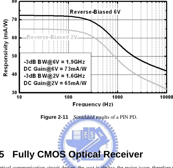
Based on physical parameters of a standard 0.18-µm CMOS technology, the calculated responsivity as functions of operating frequency is shown in Figure 2-11. For a PIN detector with DNW, the 3-dB bandwidth can be greatly promoted to 1.2 GHz and 1.9 GHz for VR = 2
V and 6 V, respectively. The results point out that the proposed PIN detector with DNW can effectively eliminate the slow diffusion response resulting from the P-substrate current. In spite of the smaller responsivity, the responsivity bandwidth product (RBW) is much better than that of a PIN detector without DNW.
21
Figure 2-11 Simulated results of a PIN PD.
2.5 Fully CMOS Optical Receiver
In optical communication circuit design, the cost is always the major issue; therefore CMOS is suitable for optical interconnection owing to the advantages of high-density and cost-effective. They can be used in short distance and high volume communication systems.
2.5.1 Optical Communication Architecture
A computing system based on high density optical link is shown in Figure 2-12. In this scenario, broad band data bus are bridged through optical links, such as the host interface between the CPU and chipset, memory data bus, and I/O interface, etc.
The goal of an optical communication system is to carry large volumes of data. Figure 2-13 denotes a typical optical communication system. Digital data is amplified, and then drives the laser source at the transmitter end. In order to have a good illuminated optical light, the laser’s
22
Figure 2-12 High density optical link for next generation CPU.
Figure 2-13 Optical transceiver architecture.
extinction-ratio (ER) will be constant, not be altered by PVT variation, the power control is needed. At the receiver end, a photodetector and a TIA translate the optical signal to a voltage data. Limiting amplifier (LA) serves as an amplitude control function to keep a constant output level, which helps the following CDR to extract the correct timing sequence.
2.5.2 Specifications of Optical Receiver
Before designing a circuit, some systematic requirements should be described. In this sub-section, some specifications of receiver front-end will be listed. Since noise, sensitivity, gain, and bandwidth of the receiver front-end dominate the performance of the overall receiver, we focus the design issues on these aspects.
23
Sensitivity and Noise
In the receiver, one of the most important requirements is its sensitivity. The sensitivity of the receiver is the minimal input power of light for a given bit error rate (BER), 10-12 for system required. The minimal accepted input power and the corresponding sensitivity can be described as:
(
)
(
)
2 , min min ( ) 10 log 2 n total pp pp SNR I P mW R P mW Sensitivity dBm ⋅ = = ⋅ (2-28) (2-29)where Pmin is the minimum input power, R is the responsivity of a photodetector, SNR
indicates a ratio of signal (peak-to-peak signal swing) to noise (root-mean-square value, which can be obtained by integrating the noise across the entire bandwidth), and In total2,
denotes the total input-referred noise current of the receiver. It can be described as:
2 , 2 2 2 , , , 2 n LA n total n PD n TIA T V I I I R = + + (2-30)
where RT denotes the gain of the transimpedance amplifier. (2-30) includes the noise
contributed from the photodetector, TIA, and LA divided by TIA transimpedance. Usually, TIA dictates this noise performance.
The Vertical-Cavity Surface-Emitting Laser (VCSEL) is a type of semiconductor laser diode and can generate the 850-nm wavelength for CMOS photodetectors. Typically, the maximum output power of VCSEL is about 0 mW or 0 dBm. Assume that the insertion loss for the short-reach communication system from transmitter end to receiver end is 6dB. The responsivity of the CMOS photodetectors (SML and PIN) is 62 mA/W. Thus, the sensitivity of the short-reach optical receiver and transimpedance amplifier will be better than -6 dBm and 31 µµµµApp, respectively. In addition, the input-referred noise of this receiver with BER less
24
Besides, the sensitivity of limiting amplifier with BER less than 10-12 is generally about 5 mVpp. Therefore, the input-referred noise of transimpedance amplifier and limiting amplifier
should be smaller than about 1.84 µµµµApp. and 0.36 mVpp, respectively.
Gain
Divide the receiver gain into three part, transimpedance gain, linear voltage gain and slicer voltage gain of limiting amplifier. In order to achieve the output swing of 800 mVpp, the conversion gain of TIA and limiting amplifier must be mare than 25.8 kΩ (or 88 dBΩ). And the transimpedance gain and linear voltage gain of limiting amplifier can be allotted 60 dBΩΩΩΩ and 28 dB for noise performance and simplification consideration. However, to have a sharper switching-logic output waveform of limiting amplifier, the additional slicer gain of 16 dB is considered.
Bandwidth
The overall receiver is designed to receive a data rate of 3.125 GHz. To avoid intersymbol interference (ISI) and must meet the sensitivity and noise requirement, the bandwidth of the overall receiver should be 2.2 GHz. Since the bandwidth of the overall receiver is determined mostly by the transimpedance amplifier. The TIA bandwidth is typically chosen to be equal to 0.7 times the bit rate under the compromise between noise and ISI. Hence, the bandwidth of the limiting amplifier (linear part) is typically designed 3.125 GHz to cause no ISI. Also, the bandwidth of the slicer part will be more than 3.125 GHz.
Table 2-3 lists the summary of the short-reach optical receiver specifications. Because the performances (responsivity of 73 mA/W and bandwidth of 1.9 GHz) of PIN detector is better than SML detector, the optical receiver can also be adopted while the PIN detector to receiver the 850-nm wavelength optical light.
25
Table 2-3 The specifications of the OEIC with SML detector.
Specifications SML PD Receiver TIA LA
(Linear)
LA (Slicer)
Gain 62mA/W 104dB 60dB 28dB 16dB
Bandwidth(GHz) 1.6 2.2 2.2 3.2 > 3.2
Sensitivity Level <-6dBm <31µApp <26µApp 5mVpp N.A.
26
Chapter 3
Transimpedance Amplifier
In optical communication system, the light transmitted by laser diode travels through a fiber and experiences loss before reaching a photodetector. The photodetector then senses the power of light and transforms the light intensity to a proportional photocurrent. At the receiver front-end, transimpedance amplifier (TIA) is an interface that converts the receiving photocurrent to electrical voltage.
In this chapter, design consideration in TIA will be introduced first. Then three typical types of preamplifier circuits are introduced and compared in section 3.2. Also, the advantages and disadvantages of two different circuit topologies (common-gate and common-source topology) will be discussed in section 3.2, too. Section 3.3 introduces the RGC-TIA chosen for meet the trade-off between large input capacitance and transimpedance gain of the TIA. And the noise analysis is also described in section3.3. Finally, the post-layout simulated results in the slow-slow (SS) corner will be shown.
27
3.1 Design Considerations
The transimpedance amplifier (TIA) is a critical block of a fiber-optic receiver. Its gain, input overload current, noise performance, bandwidth and group delay variation largely determine the overall sensitivity and the data rate of the optical link. Here we discuss the following design considerations.
Gain
The gain of TIA, or so-called transimpedance, is defined as the output voltage change per input current change. It must be large enough to overcome the noise of subsequent stage such as limiting amplifier or buffer. Besides, the gain will influence the sensitivity required for the following stage limiting amplifier indirectly. Typically, the transimpedance for 2.5 Gbps data rate is about 2k Ω to 4k Ω, and for 10 Gbps about 500 Ω to 2k Ω [10].
Input Overload Current
The input overload current is largest input current for TIA without distortions causing BER go above the level of 10-12. It defines the upper end of the TIA’s dynamic range. In SONET OC-48, the minimum required overload current is 1.6 mApp. The problem of overload characteristics enforces a gain control circuit in the TIAs [10].
Input
-
Referred Noise CurrentThe input-referred noise current of receiver front-end determines the minimum input current that yields BER be smaller than 10-12. As described in section 2.3, the TIA dictates this requirement. Typically, the input-referred noise current of TIAs for 2.5 Gbps data rate is 380 nArms and for 10 Gbps is 1400 nArms.
28
Bandwidth
In view of noise consideration, the bandwidth of TIA must be minimized so as to reduce the total integrated input-referred noise current. On the other hand, in view of intersymbol interference (ISI) in random data, the bandwidth of TIA must be maximized. The trade-off between noise and ISI makes a compromise to a bandwidth of 0.7 times the data rate. In OC-48design and OC-192, a 1.75 GHz and 7 GHz bandwidth is required at least, respectively.
Group Delay Variation
The group delay,
τ
, is related to the phase,Φ
, asτ
(ω
) = -dΦ
/dω
. The group delay variation as well as bandwidth is important parameter determining the mount of ISI and jitter introduced by the TIA. Typical values for group delay variation,∆τ
, are less than ±10% of the bit time. The∆τ
for 2.5 Gbps and 10 Gbps is about ±40 ps and ±10 ps, respectively.3.2 Preamplifier Architecture
Typically, the structure of preamplifier can be classified into three categories which are low-impedance amplifier, high-impedance amplifier and transimpedance amplifier. Here we discuss those preamplifiers on structures as well as their advantages and disadvantages in the following.
3.2.1 Architecture Comparison
Figure 3-1(a) shows a typical low-impedance preamplifier. Main advantages of the structure are (i) the preamplifier is easy to be implemented since commercially available 50Ω RF amplifier can be used; (ii) the bandwidth is large due to low RLCT time constant, (iii) it has wide input dynamic range when the signal to the preamplifier input node is at very low level.
29
(a) (b) (c)
Figure 3-1 (a) low-impedance, (b) high-impedance and (c) transimpedance preamplifier architecture.
However, the input-referred noise is high due to a low resistor at the input node.
On the contrary, the structure of high-impedance preamplifier is shown in Figure 3-1(b). Compared with low-impedance preamplifier, the equivalent input-referred noise is low due to high resistance. However, the price paid for increasing input resistance is that the bandwidth is reduced. An equalizer or other circuit is commonly used to compensate the frequency response which makes the preamplifier design more complicated.
At last, the transimpedance preamplifier is shown in Figure 3-1(c). The preamplifier frequently employs the feedback technique to enhance the bandwidth and to enlarge the dynamic range. The bandwidth is enhanced by a factor of loop gain compared with that of high-impedance preamplifier with the same load resistance and input capacitance. Besides, the noise can be very low due to large feedback resistance. One problem to be care is the stability that comes with the feedback techniques.
Table 3-1 lists the comparison of the three preamplifiers. Make a comprehensive survey of the three structures, the transimpedance amplifier is suitable for fiber-optical applications. In the transimpedance amplifier, it is desirable to achieve low noise, high transimpedance gain, and adequate bandwidth. These requirements usually conflict, requiring trade-offs to be made to suit a particular application. According to the core amplifier, transimpedance amplifier can be classified into two categories: common-source and common-gate structure.
30
Table 3-1 Comparison of three topologies of preamplifier.
Bandwidth Dynamic
Range Noise Design
Low-impedance Good Good High Easy
High-impedance Bad Bas Low Difficult
Transimpedance Good Good Low Easy
3.2.2 Circuit Topology Comparison
TIA with Common-Source Amplifier
Figure 3-2 shows a typical transimpedance amplifier with common-source core amplifier. Its transimpedance gain, TZ, and -3 dB bandwidth can be derived as:
1 1 1 -3 1 2 out m D F Z F in m IN m D dB F IN v g R R T R i g R g R R C
ω
π
= ≈ ≈ + ≈ (3-1) (3-2)Since the gain is almost equal to the feedback resistance, a larger resistance can achieve a higher gain. However, (3-2) shows that larger feedback resistance will degrade the bandwidth. In order to enhance the bandwidth, the open loop gain should be as large as possible while ensuring the stability.
In view of noise, the input-referred noise current can be described as:
2 2 2 2 2 2 2 , 2 1 2 2 2 2 1 1 2 4 1 4 1 4 1 1 4 n in m IN X IN F m D F m m D F kT kT kT I kT g C C C R g R R g g R R γ γ ω ω ω = + + + + + + (3-3)
To achieve low noise requirement, the transconductance of M1 and the resistor RF should be
as large as possible. However, these requirements conflict with input capacitance, voltage headroom, and signal bandwidth individually. One should be care is that although the noise at
31
Figure 3-2 Architecture of common source feedback amplifier.
low frequency could be negligible, that at high frequency may become considerable. For CMOS TIAs, the primary factor that constrains the bandwidth and noise performance is the inherent parasitic capacitances introduced by photodetector. As a result, in conventional common-source topology, signal bandwidth has to be severely traded-off among transimpedance gain and noise performance.
TIA with Common-Gate Amplifier
The other generally used circuit structure is with the common-gate core amplifier as shown in Figure 3-3. Compared with common-source structure, the low input impedance renders the signal bandwidth almost insensitive to parasitic capacitances introduced by photodetector. The gain and bandwidth can be described as:
2 1 2 2 1 2 1 2 1 2 -3 1
1
/
2
out m D D Z F in m D D F m m D D dB D Fv
g R R
T
R
i
g R R
R
g g R R
C R
ω
π
=
≈
≈
+
≈
(3-4) (3-5)With the same gain, the common gate topology can achieve a higher bandwidth independent of feedback resistor RF. An important drawback of common gate topologies is that they
32
Figure 3-3 Architecture of common-gate feedback amplifier.
noise thus degrading the sensitivity. The noise current spectral density can be described as:
2 2 2 , 2 2 2 1 2 2 1 4 4 4 1 1 1 4 n in mB m X F D m F D D kT kT kT I kT g g C R R γ g R R γ R ω = + + + + + + (3-6)
In order to reduce input-referred noise, the transconductance of M1, the load resistor (RD1
and RD2), feedback resistor (RF) should be chosen large. However, the load resistors will have
trade-offs with voltage headroom and signal bandwidth. Fortunately, a large feedback resistance can improve gain and noise performance at the same time while almost maintaining the signal bandwidth. On the contrary, the transconductance of current source IB should be
minimized. Under a given bias current, the gate drive voltage of IB should be increased. In
addition, the size of M2 makes trade-off between low frequency noise and high frequency
noise.
Table 3-2 Comparison of three preamplifiers.
CPD
tolerance Gain Noise
Common-Gate TIA Good Good High
33
Table 3-2 summarizes the two topologies. Although noise produced by common-gate topology is not negligible even at low frequency, its low input impedance increase the tolerance of the large photodetector capacitance. The high gain and wide bandwidth feature makes it attractive in high speed circuit design. However, the sensitivity of fully CMOS optical receiver is very important. It uses the monolithic photodetector which has very small responsivity to sense the 850-nm optical light and generate photocurrent to the TIA. Thus, the common-source topology TIA will be chosen, and the RGC input stage is utilized to reduce the large photodetector capacitance effect.
3.3 Circuit Implementation
Figure 3-4 illustrates the circuit schematic of the TIA incorporating with SML detector. It consists of two identical TIAs (M1, M3, M5 and M2, M4, M6) in a fully differential
configuration. To alleviate bandwidth degradation caused by the parasitic capacitance of the photodetector, a regulated cascode (RGC) input stage is adopted [11]. The current subtraction is performed in the second stage, which is a common source gain amplifier with shunt-shunt feedback. The voltage amplifier (M3, R3) and (M4, R4) provide a conversion gain of about 20
dB to enhance the bandwidth of the TIA, while the transimpedance gain is mainly provided by the resistors Rf1 and Rf2. The slow photocurrent (idark) collected by the dark diode is then
subtracted from that (iillu) collected by the illuminated diode in the voltage domain.
Is the supply voltage of 1.8 V appropriate for this TIA? The responsivity of the SML detector (Dillu and Ddark) is higher if the reverse-bias voltage is larger. Based on the simulation,
the reverse-bias voltage will be designed lager than 1.2 V so as to achieve better performance of SML detector. If VGS1 or VGS2 is about 0.7 V and the reverse-bias voltage of SML detector
is1.2 V, then the gate voltage of M1 or M2 is lager than 1.8 V. Thus, the supply voltage (VDD)