Effects of gate bias on hot-carrier reliability in drain extended
metal-oxide-semiconductor transistors
K. M. Wu,a兲 J. F. Chen, Y. K. Su, J. R. Lee, and K. W. Lin
Institute of Microelectronics, Department of Electrical Engineering, National Cheng Kung University, No. 1 Ta Hsueh Road, Tainan, Taiwan 70101
J. R. Shih and S. L. Hsu
Taiwan Semiconductor Manufacturing Company, Ltd., No. 121, Park Ave. 3, Science-Based Industrial Park, Hsin-Chu, Taiwan 30077
共Received 22 June 2006; accepted 19 September 2006; published online 3 November 2006兲 The effect of gate voltage on hot-carrier induced degradation in drain extended high-voltage metal-oxide-semiconductor共MOS兲 transistors with thick gate oxide 共100 nm兲 structure is presented. Different from the conventional low-voltage n-type MOS transistors, under a fixed drain voltage, devices stressed at a higher Vgs result in a greater maximum transconductance and on-resistance
degradation. Under higher Vgs, the increase in channel hot-carrier injection is responsible for the
greater Gm,maxdegradation. On the other hand, Kirk effect induced increase in drain avalanche hot carriers near the drain as well as higher electric field in the channel is responsible for the greater Ron
degradation. © 2006 American Institute of Physics.关DOI:10.1063/1.2374881兴
Drain extended metal-oxide-semiconductor 共DEMOS兲 transistors fabricated with thick gate oxide is generally used in display drivers to reduce circuit complication and chip size. Because the logic state high in display drivers usually corresponds to high drain voltage共Vds兲 and high gate voltage 共Vgs兲, hot-carrier reliability of DEMOS transistors may
be-come a serious concern. However, hot-carrier reliability of high-voltage共HV兲 DEMOS transistors was only reported for devices with thinner gate oxide 共⬍50 nm兲 operated under Vgs= 3.3– 20 V.1–4 Furthermore, there is still no consistent
conclusion concerning which Vgs 关e.g., the Vgs that
corre-sponds to peak substrate current, Isub, as in low-voltage共LV兲
metal-oxide-semiconductor field-effect transistors5 共MOS-FETs兲兴 produces the maximum degradation in HV DEMOS transistors. Such an uncertainty may underestimate the actual degradation if the stress conditions are not properly chosen. In this work, we investigate the hot-carrier reliability of thick gate oxide 共100 nm兲 HV DEMOS transistors. Experi-mental data show that higher Vgs stressing produces greater
degradation, despite the fact that Isub is not always larger under higher Vgs. Such a result indicates that the magnitude
of Isubalone may not be a good reliability indicator.
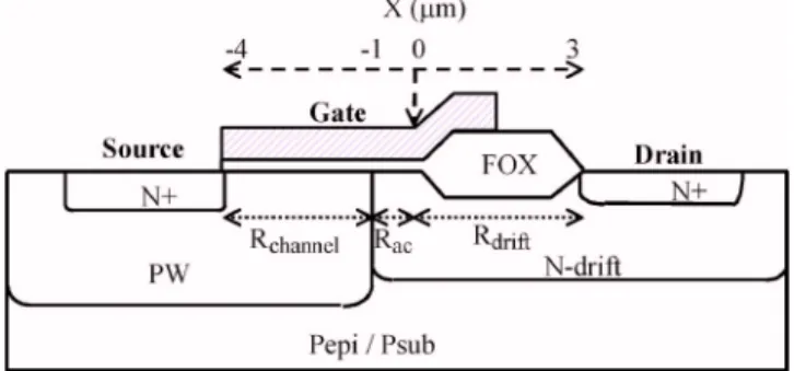
The schematic cross section of the n-type DEMOS tran-sistor used in this work is shown in Fig.1. The resistance in channel region共Rchannel兲, in accumulation region 共Rac兲, and in
the drift region共Rdrift兲 is depicted. The location of bird’s beak
共X=0m兲 is also indicated in the figure. This device was fabricated on a 0.5m complementary metal-oxide semi-conductor共CMOS兲 process with 7m pitch and features a high voltage N-drift drain extended region under the 500 nm localized oxidation of silicon field oxide共FOX兲. The polyg-ate overlaps the 100 nm gpolyg-ate oxide and extends over the field oxide. A counterdoping implant was carried out to adjust a suitable threshold voltage共Vt兲 for this thick gate oxide de-vice. The device has the following characteristics: width is
20m, net channel length is 3m, Vtis 1.5 V, normal op-erating Vdsand Vgsare 40 V, both off-state breakdown volt-age and on-state breakdown voltvolt-ages are around 60 V. Gm,max was extracted under Vds= 0.1 V. Ron was measured under Vds= 0.1 V and Vgs= 40 V. dc stressing is performed
under a wide range of Vgs at room temperature. The stress tests are interrupted periodically to measure the degradation of Gm,max and Ron. Two-dimensional technology
computer-aided-design 共TCAD兲 simulations are also performed using the SYNOPSYS software. TSUPREM4 is used for the process simulation andMEDICIis used for the device simulation.
Isuband gate current共Ig兲 as a function of Vgsfor various Vds are shown in Fig. 2. Under higher gate bias 共Vgs
⬎35 V兲, the second peak in Isuband a rapid increase in Igare
observed. The first Isubmaximum at around Vgs= 9 V is
simi-lar to the behavior in the conventional LV n-type MOSFETs. As Vgs⬎35 V, however, Isub increases again. Such a
phe-nomenon共two peaks in Isub兲 is caused by Kirk effect
共relo-cation of the high-field region under high-current condition first observed in bipolar transistors6兲 and has been reported in HV MOS transistors.7,8The Isubdata in Fig.2reveal that our DEMOS transistors exhibit a significant Kirk effect when Vgs
is high enough. Ig also increases rapidly as Vgs⬎35 V,
indi-a兲Also at: Taiwan Semiconductor Manufacturing Company, Ltd., No. 121, Park Ave. 3, Science-Based Industrial Park Hsin-Chu, Taiwan 30077; elec-tronic mail: [email protected]
FIG. 1. 共Color online兲 Schematic cross section of the high-voltage 60 V DEMOS transistor fabricated with a gate oxide thickness of 100 nm. The channel, accumulation, and drift region as well as the location of bird’s beak 共X=0m兲 are indicated in the figure.
APPLIED PHYSICS LETTERS 89, 183522共2006兲
0003-6951/2006/89共18兲/183522/3/$23.00 89, 183522-1 © 2006 American Institute of Physics Downloaded 26 Oct 2008 to 140.116.208.52. Redistribution subject to AIP license or copyright; see http://apl.aip.org/apl/copyright.jsp
cating high impact ionization generation occurring in the channel region. This could be induced by the high electron current flow through the buried-channel p-n junction and is supported by TCAD simulations shown later.
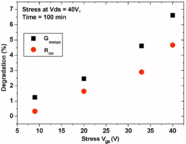
In Fig. 3, Gm,max and Ron degradation as a function of
stressing Vgsare examined for devices stressed for 100 min under Vds= 40 V. Vtshift and Id,sat degradation have similar Vgs dependence but less in magnitude are not shown in the
figure. Devices stressed under higher Vgsproduces a greater
degradation. Most reports in conventional LV n-type MOS transistors show that higher Isubresults in a greater degrada-tion. An unexpected result, however, is obtained while com-paring Figs. 2 and 3. Although Isub at Vgs= 30 V is much
smaller than the Isub at Vgs= 9 V, the degradation at Vgs
= 30 V is much greater than the degradation at Vgs= 9 V.
Note that the severity of device parameter degradation is closely related to the physical location of the damage. In concept, hot-carrier induced damage at different regions can be modeled by the increase in resistance at the corresponding region. As shown in Fig.1, the total resistance of the device can be represented by Rchannel+ Rac+ Rdrift. Hot-carrier in-duced damage in the channel region will increase Rchannel,
resulting in channel mobility degradation and is the domi-nant factor for Gm,max degradation and the secondary factor
for Ron degradation. Damage in drain n-drift region under FOX can be represented by the increase in Rdrift. Increase in
Rdriftis the primary factor to Rondegradation because Rchannel
is relatively smaller when a strong inversion channel is formed. Damage in accumulation region has a little effect on both Gm,maxand Rondegradation because Raconly increases a little due to strong gate control. The data in Fig.3reveal that hot-carrier induced damage should be significant in both channel and n-drift region when the device is stressed at higher Vgs.
To verify the above argument, TCAD simulation is per-formed to obtain the magnitude of electric field along the Si/ SiO2interface at a 0.4m depth. Vdsis fixed at 40 V and
Vgs is varied from 10 to 40 V. As shown in Fig. 4, when
Vgs= 10 V, the first peak of electric field is located close to the drain to channel n-p junction共X=−1m兲 and is similar to the case in a conventional CMOS device. The second peak of electric field 共X=0.5m兲 is close to the bird’s beak, which is due to the topography change. When Vgs= 30 and
40 V, the first peak of electric field occurs under the channel region. This significant electric field in the channel region is suspected to be due to a strong depletion in buried n-type channel under high vertical electric field because little elec-tric field is obtained if counterdoping Vt implant is not em-ployed. The second peak also occurs close to the bird’s beak. Under Vgs= 40 V, the third peak共X=3m兲 occurs close to the drain side n+ that is a strong evidence to the occurrence of Kirk effect. Compared to the conventional CMOS, this DEMOS has a field oxide inserted between drain and polyg-ate. This special structure and drain topography result in an electric field distribution that is very different from that in conventional CMOS. In our device, as Vgsis higher, the
in-crease in vertical electric field from gate to substrate occurs mostly in the channel region. This increase in vertical elec-tric field results in more channel hot-carrier injection, leading to a greater Gm,maxdegradation. On the other hand, as Vgsis higher, the increase in lateral electric field from drain to source happens mostly in the n-drift region. Further, the maximum electric field is shifted toward the drain bird’s beak due to Kirk effect. This increase in lateral electric field produces more drain avalanche hot carriers, resulting in more damage near the drain side bird’s beak and a greater Ron
FIG. 2. 共Color online兲 Substrate current 共Isub兲 and gate current 共Ig兲 as a function of Vgsunder various Vds. Under high Vgs, the second peak in Isub and a rapid increase in Igare observed.
FIG. 3.共Color online兲 Gm,maxand Rondegradation as a function of stress Vgs for devices stressed under Vds= 40 V for 100 min. Higher Vgsresults in a greater degradation.
FIG. 4.共Color online兲 TCAD simulation results on the magnitude of electric field under Vds= 40 V with various Vgs. Under higher Vgs, electric field in the channel is higher. The occurrence of Kirk effect under high Vgsis evident as the third peak in electric field close to the drain side is observed.
183522-2 Wu et al. Appl. Phys. Lett. 89, 183522共2006兲
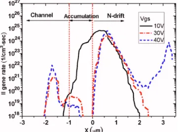
degradation. Figure5shows the simulation results of impact ionization generation rate with the same cut line as in Fig.4. When Vgs= 10 V, the center of impact ionization generation
is located underneath the bird’s beak with a broad distribu-tion, resulting in the first Isubpeak as in Fig.2. When Vgsis
higher共30 and 40 V兲, the location of peak impact ionization rate in the n-drift region is right shifted toward the drain. Furthermore, another peak occurs under the channel region, resulting in high Igas in Fig.2. The above simulation results indicate that both channel and n-drift region have significant
impact ionization generation when Vgsis higher, resulting in
higher degradation. Specifically, higher electric field in the channel from counterdoping implant is responsible for the greater Gm,max degradation. On the other hand, Kirk effect induced electric field shifted toward the drain as well as higher electric field in the channel is the cause of greater Ron
degradation.
The hot-carrier reliability of thick gate oxide 共100 nm兲 drain extended 60 V high-voltage MOS transistors was ex-amined. Results indicate that higher Vgs results in a greater
Gm,max and Ron degradation. Our findings suggest that the
behavior of hot-carrier reliability in thick gate oxide DEMOS transistors is widely different from conventional low-voltage MOSFETs. A suitable methodology to evaluate the hot-carrier reliability of DEMOS transistors is needed.
This work was partially supported by the National Sci-ence Council of Taiwan under Contract No. NSC95-2221-E006-429.
1B. J. Baliga, IEEE Trans. Electron Devices 38, 1568共1991兲.
2R. Versari and A. Pieracci, IEEE Trans. Electron Devices 46, 1228共1999兲. 3D. Brisbin, Andy Strachan, and P. Chaparala, in Proceedings of IEEE
International Reliability Physics Symposium共IEEE, New York, 2002兲, p. 105.
4S. K. Lee, C. J. Kim, J. H. Kim, Y. C. Choi, H. S. Kang, and C. S. Song, in Proceedings of IEEE ISPSD共IEEE, New York, 2001兲, p. 287. 5E. Li, E. Rosenbaum, and P. Fang, IEEE Trans. Electron Devices 48, 671
共2001兲.
6C. T. Kirk, IEEE Trans. Electron Devices 9, 164共1962兲.
7A. W. Ludikhuize, in Proceedings of IEEE ISPSD 共IEEE, New York, 1994兲, p. 249.
8A. W. Ludikhuize, M. Slotboom, A. Nezar, N. Nowlin, and R. Brock, in
Proceedings of IEEE ISPSD共IEEE, New York, 1997兲, p. 53. FIG. 5. 共Color online兲 TCAD simulation results on the impact ionization
rate under Vds= 40 V with various Vgs. Under higher Vgs, one peak of impact ionization occurs in the channel region, resulting in the greater Gm,max deg-radation. Another peak of impact ionization in n-drift region is even larger and right shifted toward the drain, resulting in the greater Rondegradation.
183522-3 Wu et al. Appl. Phys. Lett. 89, 183522共2006兲