Hydrogen-doped high conductivity ZnO films deposited by radio-frequency
magnetron sputtering
Liang-Yih Chen,a)Wen-Hwa Chen, Jia-Jun Wang, and Franklin Chau-Nan Hongb) Department of Chemical Engineering and Center for Micro-Nano Technology, National Cheng Kung University, 1 University Road, Tainan, Taiwan 701, Republic of China
Yan-Kuin Su
Department of Electrical Engineering, National Cheng Kung University, 1 University Road, Tainan, Taiwan 701, Republic of China
(Received 15 July 2004; accepted 2 November 2004)
Hydrogen-doped zinc oxide(ZnO:H) films were deposited by rf magnetron sputtering as transparent conductive films. The resistivity of ZnO:H film was significantly reduced by the addition of H2in Ar during rf sputtering. The electrical resistivity of ZnO:H films reached 2⫻10−4 ⍀ cm. The carrier concentration increased with increasing H2 concentration during deposition. X-ray diffraction results showed that the d0002interplanar spacing increased with increasing H2 concentrations. The carrier concentration was significantly reduced in two orders of magnitude by increasing the substrate temperature from 150 to 250 °C during deposition. Both results suggested that the increase of carrier concentration by adding H2during sputtering was due to the hydrogen donor rather than the oxygen vacancies in ZnO films, consistent with the theoretical predictions by Van de Walle. UV–visible spectroscopy further showed that the transmittance is high up to 100% in the visible range. The band gap determined by optical absorption increased with increasing H2 composition. The phenomenon is interpreted as the filling of conduction band by electrons in n-type semiconductor. © 2004 American Institute of Physics.[DOI: 10.1063/1.1835991]
Zinc oxide (ZnO) is a wide-band-gap semiconductor with many technological applications, including piezoelec-tric transducers, gas sensor, phosphors, and transparent con-ducting electrodes of optoelectronic devices.1–3In serving as the transparent electrode of optoelectronic devices, ZnO film owns several advantages including high transmittance in low-wavelength region, abundance in natural resource, and amorphous structure. However, it remains difficult to grow ZnO films with stable and sufficiently high conductivity. Fur-thermore, although all experimental results have shown that the undoped ZnO is n-type, whether the donor is zinc inter-stitial共Zni兲 or oxygen vacancy 共VO兲 remains controversial.
4,5 Recently, using first-principles calculation based on the density functional theory, Van de Walle6,7 has found strong evidence that hydrogen acts as a source of conductivity for ZnO. H+ is the stable and the lowest-energy state for all Fermi-level positions and can be incorporated in high con-centrations as a shallow donor in ZnO. This behavior is very different from hydrogen in other semiconductors, in which it only acts as a compensating center and always counteracts the conductivity. The above-noted prediction was experimen-tally confirmed by Cox et al.8 and Hofmann et al.9 using muon spin rotation and electron paramagnetic resonance technique, respectively. The molecular structure was further confirmed by infrared spectroscopy.10 Kiliç et al.11 general-ized the hydrogen doping behavior in various oxides recog-nizing that there exists a “hydrogen pinning level” at about 3.0± 0.4 eV below vacuum for all oxides. Van de Walle7 fur-ther suggested the existence of a universal alignment for the hydrogen energy level in various semiconductors, insulators, and even aqueous solutions.
Various post-treatment methods have been reported on the fabrication of hydrogen-doped ZnO films. Baik et al.12 treated the ZnO films deposited by metalorganic chemical vapor deposition in H2under UV illumination in a mercury-sensitized photo chemical vapor dcyosition system. The re-sistivity of the H2-treated film decreased from 1⫻10−2to 2
⫻10−3⍀ cm. Ip et al.13
investigated the electrical conduc-tivity of hydrogen in ZnO finding that exposure of ZnO to H2 plasma caused an increase in donor concentration. The effect was attributed to hydrogen passivation of acceptor impurities present in the as-grown ZnO layers.13,14 Kohiki et al. en-hanced the conductivity of ZnO film through hydrogen dop-ing by ion implantation.15 The resistivity decreased from 1 ⫻107⍀ cm for the as-grown ZnO to 1.8⫻10−3 ⍀ cm for a hydrogen doping level of 1⫻1017cm−2 .
In this study, hydrogen-doped ZnO thin films (ZnO:H) were deposited directly in a rf magnetron sputtering system
a)Electronic mail: [email protected]
b)Electronic mail: [email protected] FIG. 1. A schematic diagram of rf magnetron sputtering system.
APPLIED PHYSICS LETTERS VOLUME 85, NUMBER 23 6 DECEMBER 2004
0003-6951/2004/85(23)/5628/3/$22.00 5628 © 2004 American Institute of Physics
by incorporating H2in the sputtering gas, Ar. Figure 1 shows the schematic diagram of the sputtering system employed. The film deposition conditions are listed in Table I. The elec-trical resistivity, Hall mobility, and carrier concentration were measured at room temperature using the van der Pauw method. The crystal orientation and surface morphology were inspected by x-ray diffraction(XRD, Rigaku) and scan-ning electron microscopy Hitachi F4200), respectively. The optical transmittance was measured using an UV/visible spectrometer in a spectral range of 200–900 nm.
The electrical properties of ZnO:H films as a function of H2 compositions (in Ar) are shown in Fig. 2. The ZnO:H films are n-type with carrier concentration increased with increasing H2 composition during film deposition. The in-crease of carrier concentration can be due to the incorpora-tion of hydrogen donor of ZnO crystals by hydrogen radicals in plasma or due to the formation of oxygen vacancy by ZnO reduction with hydrogen plasma. The maximum mobility value is 40 cm2/ V s, where the carrier concentration remains high around 6⫻1020cm−3. Hall mobility increases first with increasing H2composition up to 40%, and then starts to de-crease upon further increasing H2 composition above 40%. The decrease of mobility is likely due to the increase of the density of electron scattering centers. However, the reason for the increase of mobility for a semiconductor material is that the resistivity is inversely proportional to the carrier con-centration and the carrier mobility. Thus, the lowest resistiv-ity, 2⫻10−4⍀ cm, was obtained at a H2 composition of 40%, where the mobility is at the maximum value, 39 cm2/ V s, and the carrier concentration is high around 6 ⫻1020cm−3.
XRD results in Fig. 3 show all ZnO films prepared at various H2compositions. From the inset of Fig. 3, the XRD
spectrum has only one peak around 34°. The results confirm that the ZnO:H films consisted of crystallites with preferred orientation along the c axis. The ZnO grain size is reduced by increasing H2composition during deposition, as indicated by the increase of the full width at half maximum of the peak. Besides, the(0002) peak is shifted to a lower 2value, indicating an increase of interplanar distance, d0002, with the increase of H2 composition. Previously we mentioned that the increase of carrier concentration in ZnO with increasing H2 during deposition was either due to the presence of hy-drogen donor or due to the formation of oxygen vacancy. Furthermore, Lee et al. reported that the d0002 spacing de-creased with increasing oxygen vacancy in ZnO films.16 Therefore, the observed increase of d0002 spacing with in-creasing H2composition in Fig. 3 suggests that the increase of carrier concentration must result from the increase of H donor rather than the increase of oxygen vacancy. Our results are consistent with those reported by Van de Walle, who performed extensive calculations to conclude that the H do-nor is a shallow dodo-nor in ZnO.6
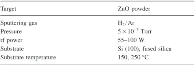
The effect of substrate temperature on the conductivity of ZnO:H thin films was also studied to investigate the be-havior of hydrogen in ZnO. Figure 4 shows the Hall mea-surement results for the ZnO:H films deposited at 150 and TABLE I. Conditions for the deposition of ZnO:H thin films.
Target ZnO powder
Sputtering gas H2/ Ar
Pressure 5⫻10−3Torr
rf power 55–100 W
Substrate Si(100), fused silica
Substrate temperature 150, 250 °C
FIG. 2. The electrical properties of ZnO:H films varied with H2composition
in Ar.
FIG. 3. X-ray diffraction patterns of ZnO:H films deposited at 150 °C sub-strate, 5 mTorr, and various H2compositions. The insert shows the ZnO:H
thin film crystallite with preferred orientation along c axis.
FIG. 4. The electrical properties of ZnO:H films deposited at 150 and 250 °C by Hall measurements.
Appl. Phys. Lett., Vol. 85, No. 23, 6 December 2004 Chenet al. 5629
250 °C. The carrier concentration is significantly higher for the film deposited at 150 °C than that at 250 °C by almost two orders of magnitude. For the film deposited at a high substrate temperature, hydrogen tends to be desorbed from the ZnO:H film inducing the increase of the resistivity. On the other hand, at a high substrate temperature oxygen might be desorbed or removed by reaction with hydrogen, forming oxygen vacancies and decreasing the resistivity of ZnO. Since the resistivity of ZnO film is observed to decrease with increasing the substrate temperature during deposition, the formation of oxygen vacancies should not be the major fac-tor in enhancing the conductivity of ZnO:H films. Therefore, our results show that hydrogen donor is responsible for the increase of carrier concentration in ZnO, as theoretically sug-gested by Van de Walle and experimentally confirmed by S Cox et al.9(a)and Hofmann et al..9(b)
In the study, UV–visible spectroscopy was also em-ployed to measure the optical transmittance of ZnO films deposited at various H2 compositions. As shown in Fig. 5, the transmittance of the as-grown ZnO film fell off steeply with decreasing wavelength around=380 nm, characteris-tic of high quality ZnO crystallites. The films are highly transparent with the transmittance in the visible region over 80%. When H2composition increases, the transmittance can be further increased up to 100%. In addition, the transmit-tance edge shifts to a lower wavelength with increasing H2 composition. The phenomenon might be due to the Burstein– Moss effect,17,18pointing out that the Fermi level inside the conduction band moves upward with increasing donor con-centration due to the filling of conduction band by the in-crease of electron carriers. The inin-crease of carrier concentra-tions in the ZnO:H films with increasing H2composition as
measured by UV–visible spectroscopy is consistent with the electrical properties by Hall measurements.
In summary, the resistivity of ZnO film is significantly reduced by the addition of H2 in Ar during rf sputtering, likely due to the hydrogen donor of ZnO. The resistivity reaches 2⫻10−4⍀ cm when H
2composition is around 40%. The corresponding carrier concentration and Hall mobility are 6⫻1020cm−3 and 38.9 cm2/ V s, respectively. XRD re-sults show that the d0002spacing increases with increasing H2 composition due to the increasing amount of hydrogen donor in ZnO crystallites. The carrier concentration in ZnO is greatly reduced by increasing the substrate temperature from 150 to 250 °C. Both results suggest that the hydrogen donor, instead of oxygen vacancies, is responsible for the increase of carrier concentrations by increasing H2concentration dur-ing deposition. They are consistent with the theoretical pre-dictions proposed by Van de Walle.6,7 The optical transmit-tance of the hydrogen-doped ZnO film is high up to 100% in the visible range. Furthermore, the transmittance edge shifts toward the lower wavelength with increasing H2composition during deposition, likely due to the Burstein–Moss effect.17,18
The work was supported by the grant from the National Science Council under the NSC-92-2214-E-006-002.
1
Y. P. Wang, W. I. Lee, and T. Y. Tseng, Appl. Phys. Lett. 69, 1807(1996).
2
D. C. Reynolds, D. C. Look, and B. Jogai, Solid State Commun. 99, 873
(1996). 3
D. M. Bagnall, Y. F. Chen, Z. Zhu, T. Yao, S. Koyama, M. Y. Shen, and T. Goto, Appl. Phys. Lett. 70, 2230(1997).
4
P. Kasai, Phys. Rev. 130, 989(1963). 5
K. Vanheusden, C. H. Seager, W. L. Warren, D. R. Tallant, and J. A. Voigt, Appl. Phys. Lett. 68, 403(1996).
6
C. G. Van de Walle, Phys. Rev. Lett. 85, 1012(2000).
7(a) C. G. Van de Walle, Physica B 308–310, 899 (2001); (b) C. G. Van de
Walle and J. Neugebauer, Nature(London) 423, 626 (2003). 8
K. Shimonura, K. Nishiyama, and R. Kasono, Phys. Rev. Lett. 89, 255505
(2002).
9(a) S. F. J. Cox, E. A. Davis, S. P. Cottrell, P. J. C. King, J. S. Lord, J. M.
Gil, H. V. Alberto, R. C. Vilão, J. Poroto Duarte, N. Ayres de Campos, A. Weidinger, R. L. Lichti, and S. J. C. Irvine, Phys. Rev. Lett. 86, 2601
(2001); (b) D. M. Holfmann, Al. Hofstaetter, F. Leiter, H. Zhou, F.
Henecher, B. K. Meyer, S. B. Orlinskii, J. Schmidt, and P. G. Baraov, ibid. 88, 045504(2002).
10
E. V. Lavrov, J. Weber, F. Börrnet, C. G. Van de Walle, and R. Helbig, Phys. Rev. B 66, 165205(2002).
11
Ç. KiliÇ and A. Zunger, Appl. Phys. Lett. 81, 73(2002).
12
S. Jae Baik, J. Hoon Jang, C. Hyun Lee, W. Yeong Cho, and K. Su Lim, Appl. Phys. Lett. 70, 3516(1997).
13
K. Ip, M. E. Overberg, Y. W. Heo, D. P. Norton, S. J. Pearton, C. E. Stutz, B. Luo, F. Ren, D. C. Look, and J. M. Zavada, Appl. Phys. Lett. 82, 385
(2003).
14(a) B. Theys, V. Sallet, F. Jomard, A. Lusson, J. -F. Rommeluere, and Z.
Teukam, J. Appl. Phys. 91, 3922 (2002); (b) C. H. Seager and S. M.
Myers, ibid. 94, 2888(2003). 15
S. Kohiki, M. Nishitani, T. Wada, and T. Hirao, Appl. Phys. Lett. 64, 2878
(1994). 16
Y. Eui Lee, J. Bin Lee, Y. Jin Kim, H. Kook Yang, J. Chul Park, and H. Joon Kim, J. Vac. Sci. Technol. A 14, 1943(1996).
17
M. K. Hudait, P. Modak, and S. B. Krupanidhi, Mater. Sci. Eng., B 56, 1
(1999). 18
N. Y. Lee, K.-J. Lee, C. Lee, J.-E. Kim, H. Y. Park, D.-H. Kwak, and H.-C. Lee, and H. Lim, J. Appl. Phys. 78, 3367(1995).
FIG. 5. Optical transmittance spectra of the ZnO:H films deposited at vari-ous H2 compositions. The inset shows the optical band gaps, determined
from the transmittance spectra, vs H2composition.
5630 Appl. Phys. Lett., Vol. 85, No. 23, 6 December 2004 Chenet al.