Properties of reactively radio frequency-magnetron sputtered „ Zr,Sn … TiO 4 dielectric films
Cheng-Liang Huang and Cheng-Hsing Hsu
Department of Electrical Engineering, National Cheng Kung University, 1 University Road, Tainan 70101, Taiwan
共Received 5 December 2003; accepted 10 April 2004兲
Zirconium tin titanium oxide doped 1 wt % ZnO thin films on n-type Si substrate were deposited by rf magnetron sputtering at a fixed rf power of 350 W with various argon-oxygen (Ar/O
2) mixture and different substrate temperatures. Electrical properties and microstructures of ZnO-doped (Zr
0.8Sn
0.2)TiO
4thin films prepared by rf magnetron sputtering on n-type Si 共100兲 substrates at different Ar/O
2ratios and substrate temperatures have been investigated. The surface structural and morphological characteristics analyzed by x-ray diffraction, scanning electron microscopy, and atomic force microscope were sensitive to the deposition conditions, such as Ar/O
2ratio 共100/0–
80/20 兲 and substrate temperature 共350 °C–450 °C兲. The selected-area diffraction pattern showed that the deposited films exhibited a polycrystalline microstructure. All films exhibited ZST 共111兲 orientation perpendicular to the substrate surface and the grain size as well as the deposition rate of the films increased with the increase of both the Ar partial pressure and the substrate temperature.
At a Ar/O
2ratio of 100/0, rf power level of 350 W and substrate temperature of 450 °C, the Zr
0.8Sn
0.2TiO
4films with 6.44 m thickness possess a dielectric constant of 42 共at 10 MHz兲, a dissipation factor of 0.065 共at 10 MHz兲, and a leakage current density of 2⫻10⫺7A/cm
2 at an electrical field of 1 kV/cm. © 2004 American Institute of Physics. 关DOI: 10.1063/1.1759085兴
I. INTRODUCTION
Development of high dielectric constant materials has been tremendously increasing in recent years. Several mate- rials, such as SrTiO
3, Ta
2O
5, and (Ba,Sr)TiO
3, are capable for applications in dynamic random access memory 共DRAM兲 and microwave communication devices.
1,2Zirconium tin ti- tanium oxide was investigated as being an useful dielectric material owing to its excellent dielectric properties, which include high dielectric constant, high quality factor, and low temperature coefficient of resonant frequency in the micro- wave regime.
3– 8Being the base material of (Zr,Sn)TiO
4, ZrTiO
4exhibits an orthorhombic crystal structure and pos- sesses ␣ -PbO type structure belonging to the Pbcn space group.
9Strong interaction forces between the ions in ZrTiO
4are weakened in solid solutions because of the decreasing number of interacting ions in the case of (Zr
1⫺XSn
X)TiO
4, and the dielectric properties of ZrTiO
4ceramics have been improved by incorporating SnO
2. With the replacement of 20 mol % Zr by Sn ions, stable dielectric properties were obtained for (Zr
0.8Sn
0.2)TiO
4ceramics.
8(Zr
0.8Sn
0.2)TiO
4ceramics possesses good dielectric properties such as high dielectric constant, high quality fac- tor, and low temperature coefficient of resonant frequency.
With the addition of 1 wt % ZnO, it has a dielectric constant of 37, which is much higher than that of SiO
2.
10A high Q
⫻ f value of 40 000 can also be achieved. That makes ZST thin films very promising in the fabrication of 共DRAMs兲.
11–14Furthermore, the temperature coefficient of resonant frequency can be adjusted to 0 ppm/ °C. It certainly can find many applications in microwave wireless communi-
cation systems such as integrated resistors or capacitors in RFICs.
In this paper, the properties of the ZnO-doped Zr
0.8Sn
0.2TiO
4thin films on n-type silicon substrate were in- vestigated at different Ar/O
2ratios 共100/0–80/20兲 and sub- strate temperatures 共300 °C–450 °C兲. The effects of the Ar/O
2ratio and substrate temperature on the crystal structure and dielectric properties of ZST films were also discussed.
II. EXPERIMENTAL PROCEDURES
The target composition (Zr
0.8Sn
0.2)TiO
4was synthesized via a conventional solid-state reaction. Starting powders of high-purity ZrO
2, SnO
2, TiO
2with 1 wt % ZnO addition were weighted and placed in polypropylene containers with milling media for 24 h in distilled water. The mixture was dried at 100 °C and thoroughly milled before it was calcined at 1000 °C for 3 h. The calcined powder was sintered at 1400 °C for 4 h. The sintered powder (Zr
0.8Sn
0.2)TiO
4was ground and sieved through 100-mesh screen to produce ZST target powder. The solid-state route was repeated twice to obtain the ZST phase and was examined by x-ray diffraction 共XRD兲, which revealed that all of the ceramics represented a single orthorhombic phase. The powder was then pressed into disk with 3 in. diameter and 6 mm thick as ZST targets.
Film deposition was prepared using rf magnetron sput- tering with a 3 in. diameter, 1 wt % ZnO-doped (Zr
0.8Sn
0.2)TiO
4powder target, as previously described. All of the films were deposited at a fixed operating pressure of 5 mTorr, which was maintained at the Ar/O
2ratio ranging from 100/0 to 80/20. With different substrate temperatures
1186
0021-8979/2004/96(2)/1186/6/$22.00 © 2004 American Institute of Physics
The deposited thin film structure was analyzed by x-ray diffraction 共Rigaku D/Max III. V兲 at 30 kV and 20 mA with Cu K ␣ radiation. The morphology of the film surface was determined using scanning electron microscopy 共SEM兲 and atomic force microscopy 共AFM兲. Moreover, the electrical properties of the ZST thin films were evaluated by capacitance-voltage (C – V) and current-voltage (I – V) mea- surements. The test samples with metal-insulator- semiconductor 共MIS兲 capacitor structures were prepared on n-type Si substrates. The sample devices 共Pt/ZST/Si/Pt兲 were fabricated by symmetrically depositing Pt electrodes 共diam- eter 0.5 mm 兲 on both sides of the ZST/Si structure. All elec- trodes were prepared by using ion sputtering. The C – V, the dissipation factor and the I – V curves of the MIS capacitors were measured by using a HP4192, a HP4294 Impedance Analyzer, and a HP4156 Parameter Analyzer, respectively.
III. RESULTS AND DISCUSSIONS
The XRD pattern of ZST thin films deposited on n-type Si 共100兲 substrates at different substrate temperatures 共350 °C–450 °C兲 with a rf power of 350 W and a Ar/O2ratio of 100/0 are shown in Fig. 1. The thin films were crystalline as deposited at substrate temperatures from 350 °C to 450 °C with Ar/O
2 ratio of 100/0. The intensities of the ZST peaks 共111兲 and 共101兲 increased as the substrate temperature in- creased. The grain growth was also enhanced with increasing substrate temperature. Since that higher substrate tempera- ture can increase the kinetic energy and mobility of the sput-
tered atoms at the growing film surface, the added energies would allow the atoms to have more chances moving to the lowest energy state.
The properties of ZST thin films were found to strongly depend on certain parameters, including substrate tempera- ture. From the XRD pattern of ZST thin films, the peaks of highly oriented ZST 共111兲 and 共101兲 were obtained. The rea- son for the orientation is determined by surface energy con- siderations. The surface energy of a crystal plane can be approximately estimated.
12␥ ⫽共pUc兲/共zN⌬S兲 共erg/cm2兲, 共1兲
where ␥ is the surface energy, Uc indicates the lattice energy, the number of bonds broken by the surface is denoted as p, z is the coordination number, and N and ⌬S represent the atomic number in the volume and the surface area, respec- tively. When the relative value of surface energy is less than the value of the other crystal plane, the orientation is deter- mined.
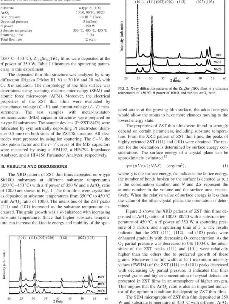
Figure 2 shows the XRD patterns of ZST thin films de- posited at Ar/O
2ratios of 100/0– 80/20 with a substrate tem- perature of 450 °C, a rf power of 350 W, a sputtering pres- sure of 5 mTorr, and a sputtering time of 3 h. The results indicate that the ZST 共111兲, 共112兲, and 共103兲 peaks were enhanced gradually with decreasing O
2concentration. As the O
2partial pressure was decreased to 0% 共100/0兲, the inten- sities of the ZST peaks 共111兲 and 共101兲 were relatively higher than the others due to preferred growth of these grains. Moreover, the full width at half maximum intensity values 共FWHM兲 of the ZST 共111兲 and 共101兲 peaks decreased with decreasing O
2partial pressure. It indicates that finer crystal grains and higher concentration of crystal defects are presented in ZST films in an atmosphere of higher oxygen.
This implies that the Ar/O
2ratio is also an important indica- tor of the optimum condition for depositing ZST thin films.
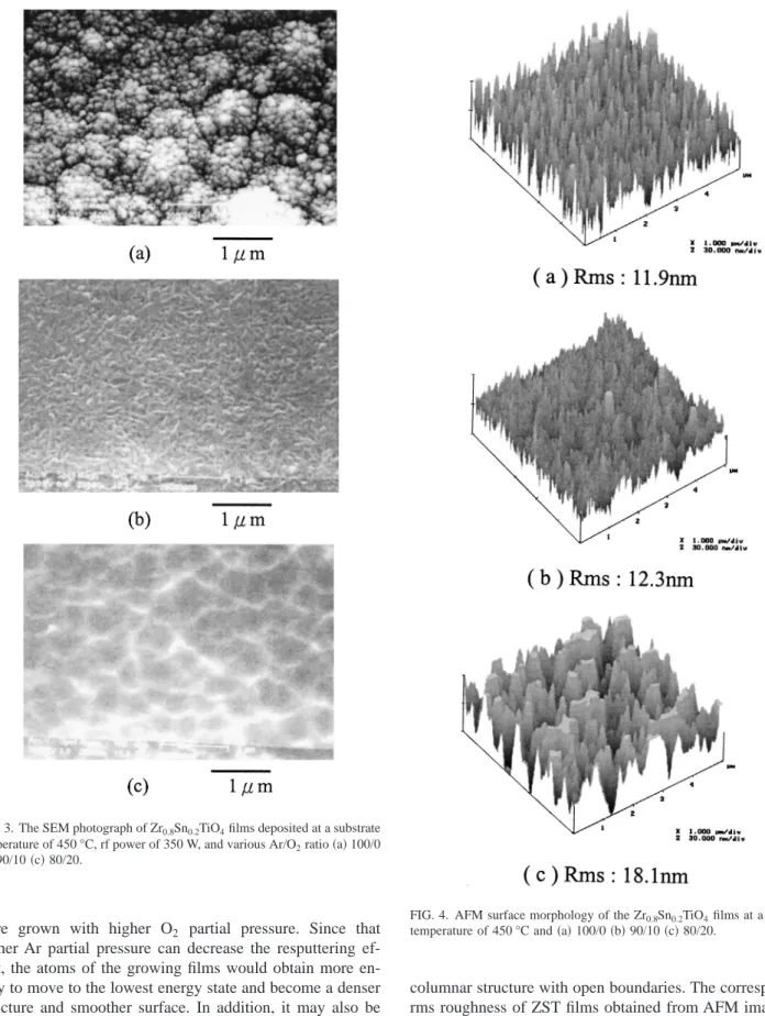
The SEM micrographs of ZST thin film deposited at 350 W and substrate temperature of 450 °C with different Ar/O
2ratios are shown in Fig. 3. The grain growth was enhanced with increasing Ar partial pressure. The finer grain crystals
FIG. 1. X-ray diffraction patterns of the Zr0.8Sn0.2TiO4films at a rf power of 350 W, Ar/O2ratio of 100/0, and various substrate temperature.
FIG. 2. X-ray diffraction patterns of the Zr0.8Sn0.2TiO4films at a substrate temperature of 450 °C, rf power of 100/0, and various Ar/O2ratio.
were grown with higher O
2partial pressure. Since that higher Ar partial pressure can decrease the resputtering ef- fect, the atoms of the growing films would obtain more en- ergy to move to the lowest energy state and become a denser structure and smoother surface. In addition, it may also be the greater oxygen content in the sputtering gas mixture causes low gas ionization effect so that the surface morphol- ogy of the growing film is not uniform.
Figure 4 illustrates the surface morphology of the films deposited at a fixed rf power of 350 W, a substrate tempera- ture of 450 °C with various Ar/O
2ratios. It indicates that the root-mean-square 共rms兲 roughness of the films increased as the Ar partial pressure decreased, and the films exhibited
columnar structure with open boundaries. The corresponding rms roughness of ZST films obtained from AFM images re- veals that the surface roughness increased from 11.9 nm to 18.1 nm as the O
2concentration increased from 0% to 20%.
This result may be attributed to that the greater oxygen con- tent in the sputtering gas mixture causes a more serious re- sputtering effect, which damages the surface morphology of the growing film. In addition, the mobility of the atom is reduced with increasing oxygen. In the case of various Ar/O
2ratios of mixed sputtering gas, 0% oxygen concentration pro-
FIG. 3. The SEM photograph of Zr0.8Sn0.2TiO4films deposited at a substrate temperature of 450 °C, rf power of 350 W, and various Ar/O2ratio共a兲 100/0 共b兲 90/10 共c兲 80/20.
FIG. 4. AFM surface morphology of the Zr0.8Sn0.2TiO4films at a substrate temperature of 450 °C and共a兲 100/0 共b兲 90/10 共c兲 80/20.
duced films with denser structure and smoother surface.
Figure 5 is the cross-sectional SEM micrographs of ZST thin films deposited at different Ar/O
2ratios 共from 100/0 to 80/20 兲 with a substrate temperature of 450 °C, a rf power of 350 W, a sputtering pressure of 5 mTorr, and a sputtering time of 3 h. It is observed that the thickness of the thin film increased with increasing Ar partial pressure. Moreover, it also shows a continuous stack structure, implying a good adhesion between film and substrate. The FWHM of the ZST peak decreased with decreasing O
2partial pressure; that is,
the crystallization of ZST thin films was improved with de- creasing O
2partial pressure. This implies that the Ar/O
2ratio is an important indicator of the optimum condition for depo- sition of ZST thin films.
The C – V behavior of ZST films was measured via a Pt/ZST/Si/Pt 共MIS兲 structure. In the measurement of capaci- tance voltage at 10 MHz, the applied dc voltage was swept from ⫺5 V to 5 V. All of the results of the C – V curve 共Fig.
6 兲 were shown in the fiat-band voltage. By using the fiat- band characteristic caused by the measuring process itself, the dielectric constant of the ZST films can be calculated from the values of the accumulation capacitance. The depo- sition rate and the dielectric constant of the ZnO-doped ZST films as a function of Ar/O
2ratio is demonstrated in Fig. 7.
The deposition rate of the films increased from 17 to 41
FIG. 5. The cross-sectional SEM photograph of the Zr0.8Sn0.2TiO4 films deposited at rf power of 350 W, a substrate temperature of 450 °C, and various Ar/O2ratio共a兲 100/0 共b兲 90/10 共c兲 80/20.
FIG. 6. The C – V curve of the Pt/Zr0.8Sn0.2TiO4/Si(100) MIS structure with different Ar/O2ratio at rf power of 350 W and substrate temperature of 450 °C.
FIG. 7. The dielectric constant and deposition rate of Zr0.8Sn0.2TiO4 thin films on various Ar/O2ratio at rf power of 350 W and substrate temperature of 450 °C.
nm/min as the O
2partial pressure increased from 0%
(Ar/O
2⫽100/0) to 20% (Ar/O
2⫽80/20) at 450 °C. At con- stant substrate temperature 共450 °C兲, higher deposition rate was obtained at a higher Ar partial pressure 共100/0兲 due to higher mobility of the deposited atoms. Moreover, the dielec- tric constant of the ZST films also increased with increasing Ar partial pressure. The dielectric constant is influenced by the grain size and the crystallinity. From the XRD patterns, intensities of the ZST peaks 共111兲 and 共101兲 was increased with increasing substrate temperature and rf power. It shows an improvement in the crystallinity of the films. With Ar/O2
ratio of 100/0, rf power of 350 W and substrate temperature of 450 °C, a dielectric constant of 42 was obtained.
Figure 8 shows the I – V curves of the ZST films depos- ited on n-type Si substrate with different Ar/O
2ratios at a fixed rf power of 350 W and a substrate temperature of 450 °C. The results of measurements were fit with leakage current density vs electrical field. The leakage current den- sity decreased with increasing Ar partial pressure. The leak- age current is influenced by the grain size, the crystallinity, and the surface morphology. The grain boundary structure is more dense and more uniform with increasing Ar partial pressure. In addition, decreasing the crystal defect and in- creasing the grain size was also produced with increasing Ar partial pressure. A leakage current density of 2
⫻10
⫺7A/cm
2was obtained near an electrical field of 1 kV/cm with a Ar/O
2ratio of 100/0, a rf power of 350 W and a substrate temperature of 450 °C, which is very similar to the leakage current density of SiO
2.
The dissipation factor or loss tangent is defined as tan ␦
⫽ ⬘ / ⬙ ⫽k ⬘ /k ⬙ , which is a result from the leakage current through the loss by a parallel resistance. Therefore, the loss tangent increases as the resistance decreases or leakage cur- rent increases. Figure 9 shows the dependence of frequency of ZST films on dissipation factor with different Ar/O2 ra- tios. As the Ar partial pressure increased, the dissipation fac- tors decreased owing to the uniform thin film morphology.
Moreover, with the increase in frequency, dissipation factor increased owing to the increase in dielectric and conductor losses. With Ar/O
2ratio of 100/0, substrate temperature of
450 °C and rf power of 350 W, a dissipation factor of 0.065 was measured at 10 MHz.
IV. CONCLUSION
Crystalline of 1 wt % ZnO-doped ZST thin films depos- ited on Si 共100兲 by rf magnetron sputtering was investigated.
The Ar/O
2ratio and substrate temperature were important parameters in the sputtering process. As the substrate tem- perature and Ar concentration increased, the quality of the ZST thin films was improved since the kinetic energies of the sputtered atoms increased resulting in a structural improve- ment. The intensities of the peaks ZST 共111兲 and 共002兲 de- posited at Ar/O
2ratio of 100/0 and substrate temperature of 450 °C were higher than others. Grain growth was also en- hanced with the increase of both Ar concentration and sub- strate temperature. The deposition rate of the films increased with an increase in Ar concentration. By properly adjusting the Ar/O
2ratio, one can precisely control the deposition rate at constant rf power. In addition, the surface roughness of the thin films decreased with increasing oxygen concentration in the sputtering gas mixture. The optimum conditions for the growth of ZST thin films in this study were a substrate tem- perature of 450 °C, a Ar/O
2ratio of 100/10, and a sputtering time of 3 h. A high dielectric constant of 42 ( f ⫽10 MHz), dissipation factor of 0.065 ( f ⫽10 MHz) and a low leakage current density of 2 ⫻10⫺7 A/cm
2were obtained for the pre- pared films. It may find applications in dynamic random ac- cess memories and wireless communication devices.
ACKNOWLEDGMENT
This work was supported by the National Science Coun- cil of the Republic of China under Grant No. NSC-92-2213- E-006-064.
1C. S. Hwang, S. O. Park, H. J. Cho, C. S. Kang, H. K. Kang, S. I. Lee, and M. Y. Lee, Appl. Phys. Lett. 67, 2819共1995兲.
2H. Matsuhashi and S. Nishikawa, Jpn. J. Appl. Phys., Part 1 33, L293 共1994兲.
FIG. 8. The I – V curve of the Pt/Zr0.8Sn0.2TiO4/Si(100) MIS structure with different Ar/O2 ratio at substrate temperature of 450 °C and rf power of 350 W.
FIG. 9. Dependence of frequency of ZST films on dissipation factor with various Ar/O2 ratio 共rf power of 350 W and substrate temperature of 450 °C兲.