Photoluminescence and photoreflectance study of annealing effects on
GaAs
0.909Sb
0.07N
0.021layer grown by gas-source molecular beam epitaxy
Hung-Pin Hsu,1Yen-Neng Huang,1Ying-Sheng Huang,1,a兲 Yang-Ting Lin,2Ta-Chun Ma,2 Hao-Hsiung Lin,2Kwong-Kau Tiong,3Piotr Sitarek,4and Jan Misiewicz4
1
Department of Electronic Engineering, National Taiwan University of Science and Technology, Taipei 106, Taiwan
2Department of Electrical Engineering, National Taiwan University, Taipei 106, Taiwan
3Department of Electrical Engineering, National Taiwan Ocean University, Keelung 202, Taiwan 4Institute of Physics, Wrocław University of Technology, Wybrzeże Wyspiańskiego 27, 50-370 Wrocław, Poland
共Received 22 January 2008; accepted 18 March 2008; published online 9 June 2008兲
Thermal annealing effects of a GaAs0.909Sb0.07N0.021film grown on GaAs substrate via gas-source molecular beam epitaxy have been characterized by photoluminescence共PL兲 and photoreflectance 共PR兲 techniques. PL measurements show the evolution of luminescence feature with the thermal annealing treatment. The conduction to heavy-hole 共HH兲 band and conduction to light-hole 共LH兲 band transitions originated from the strained induced valence band splitting in GaAs0.909Sb0.07N0.021 layer have been observed by the PR measurements. The near band edge transition energies are slightly blueshifted, and the splitting of HH and LH bands is reduced with rising annealing temperature. The temperature dependences of near band edge transition energies are analyzed using Varshni and Bose–Einstein expressions in the temperature range from 15 to 300 K. The parameters that describe the temperature variations of the near band edge transition energies are evaluated and discussed. © 2008 American Institute of Physics.关DOI:10.1063/1.2927490兴
I. INTRODUCTION
The nitride III-V semiconductors alloys such as GaNAs and GaInNAs have attracted a lot of attentions in recent past due to their unique physical properties and potential applica-tions for achieving the telecommunication wavelengths of 1.3– 1.55m with GaAs-based materials.1–4 In order to achieve the emission wavelength beyond 1.3m, many N atoms must be incorporated into the Ga共In兲As alloy which can result in degradation of crystal quality of such materials.5 In order to guarantee the performance of dilute nitride mate-rials, the N composition in the range of 0%–2%, commonly around 1% for Ga共In兲NAs alloys, is suggested.6
Recently, Ungaro et al.7 proposed an alternative alloy, namely, GaAsSbN which offers capability to achieve longer wave-length with lower N concentration compared to GaInNAs. Their works demonstrate that the GaAsSbN grown on GaAs substrate can be used to prepare optical devices emitting in 1.3– 1.5m region at room temperature.8–10The studies re-lated to GaAsSbN applications in long wavelength optical devices have also been reported.11–13 However, in spite of their potential applications, very little work has been done on the optical properties related to thermal annealing effects in such a quaternary material. For example, the optical transi-tion features originated from the valence band splitting and their temperature dependent near band edge interband tran-sitions properties is only little known. Hence, further study on the thermal annealing effects of GaAsSbN alloy is not only interesting but also necessary and important.
In this work we present the photoluminescence共PL兲 and
photoreflectance共PR兲 study of thermal annealing effects on a strained GaAs0.909Sb0.07N0.021layer grown on GaAs substrate by gas-source molecular beam epitaxy共MBE兲. The conduc-tion to heavy-hole 共HH兲 band and conduction to light-hole 共LH兲 band transitions originated from strain induced valence band splitting have been observed. The temperature depen-dence behaviors of these transition energies in the range from 15 to 300 K are also studied. The parameters that de-scribe the temperature variations of the near band edge tran-sition energies are evaluated and discussed.
II. EXPERIMENT
The GaAs0.909Sb0.07N0.021 layer was grown on 共100兲 semi-insulating GaAs substrate via a VG-V80 gas-source MBE system. An EPI Sb cracking cell was used to provide mixed dimmer and monomer Sb beam. The source of As2 beam was from a gas cell with a cracking temperature of 1000 ° C using AsH3 as the precursor. Gallium flux, cali-brated using an ion gauge to keep the growth rate at 1m/h, was provided by an EPI unibulb rf plasma K-cell operating at a radio frequency of 13.56 MHz. A shutter was placed in front of the K-cell to reduce the ionized species. The thick-ness of the samples in this study was 1m with growth temperature of 490 ° C. The composition of the GaAs0.909Sb0.07N0.021was quantified by electron probe x-ray microanalyzer with GaAs, GaN, and GaSb as standards for ZAF 共atomic number Z, absorption A, and fluorescence F兲 correction. The samples were ex situ annealed at tempera-tures of 800 and 850 ° C for 300 s in N ambient during the thermal annealing process.
In PL measurements, the signal was collected by a spec-trometer and detected by an InGaAs charge coupled device a兲Author to whom correspondence should be addressed. Electronic mail:
ysh@mail.ntust.edu.tw.
array. A 60 mW double frequency neodymium doped yttrium aluminum garnet 532 nm green laser was employed as the excitation source. For PR measurement, the modulation of the built-in electric field is caused by photoexcited electron-hole pairs created by a mechanically chopped 670 nm line 共⬃3 mW兲 of a laser diode with a modulating frequency at 200 Hz. The radiation from a 150 W tungsten-halogen lamp filtered by a 0.25 m monochromator provided the monochro-matic light. The reflected light was detected by an InGaAs photodetector. The dc output of photodetector was main-tained constant by a servomechanism of variable neutral den-sity filter. A dual-phase lock-in amplifier was used to mea-sure the detected signals. Multiple scans over a given photon energy range were programmed until a desired signal-to-noise level has been attained with computer controlled data acquisition procedure. Detailed PR configuration has been described elsewhere.14,15 For temperature dependent mea-surements, a closed-cycle cryogenic refrigerator equipped with a digital thermometer controller with a temperature sta-bility better than 0.5 K was used.
III. RESULTS AND DISCUSSION
Figure 1 depicts the PL spectra of the annealed GaAs0.909Sb0.07N0.021samples at 15 K. The PL peak energies were determined to be 1.005 and 1.063 eV for samples an-nealed at 800 and 850 ° C, respectively, and no luminescence recorded for the as-grown sample. The PL spectrum for sample annealed at 800 ° C revealed a broad signal at lower energy, and the signal quality of this commonly observed feature for dilute nitride compound showed vast improve-ment via annealing at 850 ° C. As shown in Fig. 1, the PL peak position blueshifted together with a narrowing of the full width at half maximum and increases in the intensity with rising thermal annealing temperature. The PL results did imply that the luminescence properties can be improved by thermal annealing. Nevertheless, the PL signal usually af-fected by the localized clusters due to the alloy disorder in dilute nitride system which may not give us correct
informa-tion on near band edge transiinforma-tions. In the following secinforma-tion, we have used PR technique to characterize the near band edge transitions with higher accuracy.
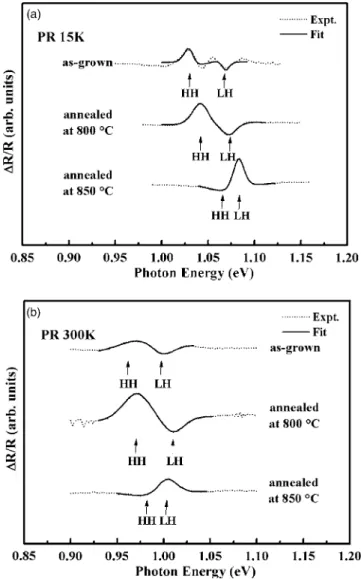
Figure 2 shows PR spectra for the as-grown GaAs0.909Sb0.07N0.021 sample and samples annealed at 800 and 850 ° C at共a兲 15 K and 共b兲 room temperature. The dot-ted lines are the experimental data and full curves are the least-squares fits to the first-derivative Lorentzian line-shape function of the form16
⌬R
R = Re
兺
j=1Ajei⌽j共E − Ej+ i⌫j兲−n, 共1兲 where Aj and ⌽j are the amplitude and phase of the line shape, Ejand⌫jare the energy and broadening parameter of the transitions, and the value of n depends on the origin of the transitions. For the derivative functional form, n = 2 is appropriate for the bound states such as excitons. The ob-tained near band edge transitions are indicated by vertical arrows and denoted as HH and LH for conduction to HH band and conduction to LH band transitions originated from strain induced valence band splitting. As annealing tempera-FIG. 1. The PL spectra at 15 K for the GaAs0.909Sb0.07N0.021samples
an-nealed at 800 and 850 ° C.
FIG. 2. Experimental PR spectra 共dotted curves兲 for as-grown and two annealed GaAs0.909Sb0.07N0.021samples at共a兲 15 and 共b兲 300 K. The full
lines are least-squares fits to Eq.共1兲. The obtained values of the transition energies are indicated by the arrows.
ture rises, two effects can be noticed: a slight blueshift of the transitions and the reduced separation of HH and LH transi-tions. The separations between HH and LH transitions are 37, 32, and 19 meV for as-grown sample and samples
an-nealed at 800 and 850 ° C, respectively. The results show that strain in GaAsSbN layer can be reduced after thermal an-nealing treatment.
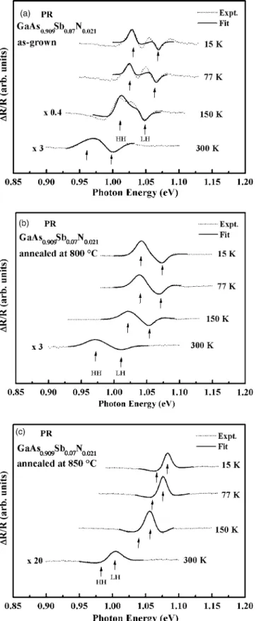
Displayed by dotted curves in Figs. 3共a兲–3共c兲 are, re-spectively, the experimental PR spectra of as-grown and samples annealed at 800 and 850 ° C, at several temperatures FIG. 3. Experimental PR spectra共dotted curves兲 of GaAs0.909Sb0.07N0.021共a兲
as-grown sample and samples annealed at共b兲 800 and 共c兲 850 °C at several temperatures between 15 and 300 K. The full curves are least-squares fits to Eq.共1兲. The obtained values of the transition energies are indicated by the arrows.
FIG. 4. Temperature variations of the experimental PR values for electron to HH and LH transitions with representative error bars for GaAs0.909Sb0.07N0.021共a兲 as-grown sample and samples annealed at 共b兲 800
and共c兲 850 °C as open squares and circles, respectively. The full curves are least-squares fits to Eq.共2兲and the dotted curves are least-squares fits to Eq. 共3兲.
between 15 and 300 K. The solid lines are the fitted spectral data to Eq. 共1兲 with n = 2, which yield transition energies indicated by arrows. As the general property of most semi-conductors, when the measuring temperature is increased, the HH and LH transitions in the PR spectra exhibit an en-ergy redshift characteristic.
The temperature variations of the experimental PR val-ues for HH and LH transitions with representative error bars for as-grown GaAs0.909Sb0.07N0.021sample and samples an-nealed at 800 and 850 ° C are depicted in Figs.4共a兲–4共c兲as open squares and circles, respectively. The full curves are the temperature dependence of the HH and LH near band edge transition energies fitted by Varshni semiempirical relationship,17
Ei共T兲 = Ei共0兲 − ␣iT2
i+ T, 共2兲
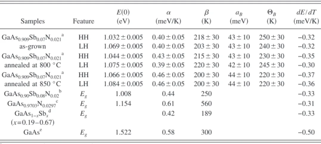
where Ei共0兲 is the conduction to HH or LH band transition energies at 0 K. The constants ␣i is related to the electron 共exciton兲-average phonon interaction strength and i is closely related to the Debye temperature. The values ob-tained are listed in TableI. For comparison, the parameters for band gap energies of GaAs0.90Sb0.08N0.02,18 GaAs0.9703N0.0297,19GaAs1−xSbx,20and GaAs21are also listed in TableI.
The temperature dependence of near band edge transi-tion energies can also be described by a Bose–Einstein ex-pression共dotted curves兲22,23
Ei共T兲 = Ei共0兲 −
2aiB 关exp共⌰iB/T兲 − 1兴
, 共3兲
where Ei共0兲 is the transition energies for the conduction to HH or conduction to LH band transition energies at 0 K, aiB represents the strength of the electron共exciton兲-average pho-non interaction, and⌰iBcorresponds to the average phonon temperature. The values obtained for the various parameters
are also presented in TableI, together with that of the param-eters for band gap energies of GaAs0.90Sb0.08N0.02,18 GaAs0.9703N0.0297,19 GaAs1−xSbx,20 and GaAs21 for compari-son.
The parameter␣ of Eq.共2兲 can be related to aBand⌰B in Eq. 共3兲 by taking the high temperature limit of both ex-pressions. This yields ␣= 2aB/⌰B. The comparison of the numbers presented in TableIshow that this relation is fairly satisfied. From Eq.共3兲, it is straightforward to show that high temperature limit of the slope of E共T兲 versus T curve ap-proaches a value of −2aB/⌰B. The calculated value of −2aB/⌰B for conduction to HH共LH兲 near band edge transi-tion energies equals to −0.34 共−0.35兲, −0.37 共−0.34兲, and −0.40共−0.40兲 meV/K for as-grown sample and samples an-nealed at 800 and 850 ° C, respectively, which agrees well with the value of 关dEHH共LH兲/dT兴=−0.32 共−0.32兲, −0.35 共−0.30兲, and −0.37 共−0.36兲 meV/K as obtained from the lin-ear extrapolation of the high temperature 共150–300 K兲 PR experimental data.
As shown in Table I, the parameters that describe the temperature variations of near band edge transition energies of GaAs0.909Sb0.07N0.021 alloys are quite similar to that re-ported by Bian et al.18 The values of ␣ and dE/dT for GaAs0.909Sb0.07N0.021are similar to that of GaAs0.9703N0.0297 共Ref. 19兲 and GaAs1−xSbx 共Ref. 20兲 films and smaller than that of GaAs. The temperature induced shift of the band edge transition energies has been illustrated to be substantially re-duced by the presence of nitrogen/antimony.
IV. SUMMARY
In summary, we have studied thermal annealing effects of a dilute nitride GaAs0.909Sb0.07N0.021film grown on GaAs substrate with different thermal annealing temperatures by PL and PR techniques. The PL results show that the lumi-nescence feature blueshifted and the intensity increased to-gether with a narrowing of the feature by thermal annealing TABLE I. Values of the Varshni- and Bose–Einstein–type fitting parameters, which describe the temperature
dependence of near band edge transition energies for as-grown GaAs0.909Sb0.07N0.021alloy and samples annealed
at 800 and 850 ° C. The parameters of GaAs0.90Sb0.08N0.02, GaAs0.9703N0.0297, GaAs1−xSbx, and GaAs are also included for comparison.
Samples Feature E共0兲 共eV兲 共meV/K兲␣ 共K兲 aB 共meV兲 共K兲⌰B dE/dT 共meV/K兲 GaAs0.909Sb0.07N0.021a as-grown HH LH 1.032⫾0.005 1.069⫾0.005 0.40⫾0.05 0.40⫾0.05 218⫾30 203⫾30 43⫾10 43⫾10 250⫾30 240⫾30 −0.32 −0.32 GaAs0.909Sb0.07N0.021a annealed at 800 ° C HH LH 1.044⫾0.005 1.075⫾0.005 0.43⫾0.05 0.39⫾0.05 215⫾30 220⫾30 43⫾10 42⫾10 230⫾30 245⫾30 −0.35 −0.30 GaAs0.909Sb0.07N0.021a annealed at 850 ° C HH LH 1.066⫾0.005 1.084⫾0.005 0.46⫾0.05 0.46⫾0.05 200⫾30 200⫾30 44⫾10 44⫾10 220⫾30 220⫾30 −0.37 −0.36 GaAs0.90Sb0.08N0.02b Eg 1.008 0.44 250 −0.33 GaAs0.9703N0.0297c Eg 1.154 0.61 560 −0.31 GaAs1−xSbxd 共x=0.19–0.67兲 Eg 0.42 189 −0.33 GaAse Eg 1.522 0.58 300 −0.50
aPresent work共photoreflectance兲. bReference18共photoluminescence兲. cReference19共absorption兲. dReference20共absorption兲. eReference21共absorption兲.
at higher temperature. From the PR results, the HH and LH transitions originated from the strained induced valence band splitting in the GaAs0.909Sb0.07N0.021 layer have been ob-served. The near band edge transition energies are slightly blueshifted, and the splitting of HH and LH bands is reduced with rising thermal annealing temperature. The temperature dependences of these near band edge transition energies are analyzed using the Varshni expression and an expression containing the Bose–Einstein occupation factor for phonons. The parameters that describe the temperature dependences of GaAsSbN alloy are similar to that of GaAs0.9703N0.0297 and GaAs1−xSbx and smaller than that of GaAs. This has been attributed to the incorporation of nitrogen/antimony into the GaAsSbN alloys
ACKNOWLEDGMENTS
The authors acknowledge the supports of National Sci-ence Council of Taiwan under Project No. NSC 96-2221-E-011-030 and the project-based personnel exchange pro-gramme between the NSC and PAS Project No. NSC96-2911-I-011-003.
1M. Kondow, K. Uomi, A. Niwa, T. Kitatani, S. Wataniki, and Y. Yazama, Jpn. J. Appl. Phys., Part 135, 1273共1996兲.
2T. Kitatani, K. Nakahara, M. Kondow, K. Uomi, and T. Kitatani,Jpn. J. Appl. Phys., Part 239, L86共2000兲.
3C. W. Tu,J. Phys.: Condens. Matter13, 7169共2001兲.
4K. Uesugi, N. Morooka, and I. Suemune, Appl. Phys. Lett. 74, 1254
共1999兲.
5L. F. Bian, D. S. Jiang, and S. L. Lu,J. Cryst. Growth253, 155共2003兲.
6M. Fischer, M. Reinhardt, and A. Forchelm, Electron. Lett. 36, 1208
共2000兲.
7G. Ungaro, G. Le Roux, R. Teissier, and J. C. Harmand,Electron. Lett.35,
1246共1999兲.
8J. C. Harmand, G. Ungaro, L. Largeau, and G. Le Roux,Appl. Phys. Lett. 77, 2482共2000兲.
9J. C. Harmand, G. Ungaro, J. Ramos, E. V. K. Rao, G. Saint-Girons, R.
Teissier, G. Le Roux, L. Largeau, and G. Patriarche, J. Cryst. Growth
227–228, 553共2001兲.
10J. C. Harmand, A. Caliman, E. V. K. Rao, L. Largeau, J. Ramos, R.
Teissier, L. Travers, G. Ungaro, B. Theys, and I. F. L. Dias,Semicond. Sci. Technol.17, 778共2002兲.
11S. Wicaksono, S. F. Yoon, W. K. Loke, K. H. Tan, K. L. Lew, M. Zegaoui,
J. P. Vilcot, D. Decoster, and J. Chazelas,J. Appl. Phys. 102, 044505
共2007兲.
12K. H. Tan, S. F. Yoon, W. K. Loke, S. Wicaksono, K. L. Lew, A. Stöhr, O.
Ecin, A. Poloczek, A. Malcoci, and D. Jäger,Appl. Phys. Lett.90, 183515
共2007兲.
13H. Luo, J. A. Gupta, and H. C. Liu,Appl. Phys. Lett.86, 211121共2005兲. 14Y. S. Huang and F. H. Pollak,Phys. Status Solidi A202, 1193共2005兲. 15F. H. Pollak and H. Shen, Mater. Sci. Eng., R. 10, xv共1993兲.
16D. E. Aspnes, in Handbook on Semiconductors, edited by M. Balkanski
共North-Holland, Amsterdam, 1980兲, Vol. 2, p. 109.
17Y. P. Varshni,Physica共Amsterdam兲34, 149共1967兲.
18L. F. Bian, D. S. Jiang, P. H. Tan, S. L. Lu, B. Q. Sun, L. H. Li, and J. C.
Harmand,Solid State Commun.132, 707共2004兲.
19K. Uesugi, I. Suemune, T. Hasegawa, T. Akutagawa, and T. Nakamura, Appl. Phys. Lett.76, 1285共2000兲.
20R. Lukic-Zrnic, B. P. Gorman, R. J. Cottier, T. D. Golding, C. L. Littler,
and A. G. Norman,J. Appl. Phys.92, 6939共2002兲.
21M. B. Panish and H. C. Casey, Jr.,J. Appl. Phys.40, 163共1969兲. 22P. Lautenschlager, M. Garriga, and M. Cardona,Phys. Rev. B36, 4813
共1987兲.
23P. Lautenschlager, M. Garriga, S. Logothetidis, and M. Cardona,Phys. Rev. B35, 9174共1987兲.