國 立 交 通 大 學
電子工程學系 電子研究所碩士班
碩 士 論 文
應用於低溫多晶矽製程下
應用於低溫多晶矽製程下
應用於低溫多晶矽製程下
應用於低溫多晶矽製程下電容式感測器
電容式感測器
電容式感測器
電容式感測器讀出
讀出
讀出電
讀出
電
電
電
路設計與實現
路設計與實現
路設計與實現
路設計與實現
Design and Realization of Capacitive Sensor
Readout Circuit in LTPS Technology
研 究 生: 林佑達 (Yu-Ta Lin)
指導教授: 柯明道教授 (Prof. Ming-Dou Ker)
應用於低溫多晶矽製程下
應用於低溫多晶矽製程下
應用於低溫多晶矽製程下
應用於低溫多晶矽製程下電容式感測器
電容式感測器
電容式感測器
電容式感測器讀出
讀出
讀出
讀出
電路設計與實現
電路設計與實現
電路設計與實現
電路設計與實現
Design and Realization of Capacitive Sensor
Readout Circuit in LTPS Technology
研 究 生:林佑達
Student: Yu-Ta Lin
指導教授:柯明道教授
Advisor: Prof. Ming-Dou Ker
國立交通大學
電子工程學系
電子研究所
碩士論文
A Thesis
Submitted to Department of Electronics Engineering and Institute of Electronics
College of Electrical and Computer Engineering
National Chiao-Tung University
in Partial Fulfillment of the Requirements
for the Degree of
Master
in
Electronics Engineering
September 2010
Hsin-Chu, Taiwan
中華民國九十九年九月
應用於低溫多晶矽製程下
應用於低溫多晶矽製程下
應用於低溫多晶矽製程下
應用於低溫多晶矽製程下
電容式感測器
電容式感測器
電容式感測器
電容式感測器讀出
讀出
讀出電路
讀出
電路
電路
電路設計與實現
設計與實現
設計與實現
設計與實現
學生
學生
學生
學生:
:
:林佑達
:
林佑達
林佑達
林佑達
指導教授
指導教授
指導教授:
指導教授
:
:
:柯明道教授
柯明道教授
柯明道教授
柯明道教授
國立交通大學
國立交通大學
國立交通大學
國立交通大學 電子工程學系電子研究所
電子工程學系電子研究所
電子工程學系電子研究所碩士班
電子工程學系電子研究所
碩士班
碩士班
碩士班
ABSTRACT (CHINESE)
低 溫 多 晶 矽 (low temperature polycrystalline silicon, LTPS) 薄膜 電晶 體 (thin-film transistors, TFTs) 已被視為一種材料廣泛地研究於可攜帶式系統產品 中,例如數位相機、行動電話、個人數位助理 (PDA) 、筆記型電腦等,這是由 於低溫多晶矽薄膜電晶體的電子遷移率約是傳統非晶矽 (amorphous silicon) 薄 膜電晶體的一百倍大。此外,低溫多晶矽技術可藉由將驅動電路整合於顯示器之 周邊區域來達到輕薄、巧小且高解析度的顯示器。這樣的技術也將越來越適合於 系統面板 (System-on-Panel, SOP) 應用之實現。
隨著系統面板的發展,各式輸入顯示技術 (input display technology) 被整合 於其中,包含了記錄文字、影像或是照片的掃描器 (scanner),偵測手指或是筆 跡的觸控式面板 (touch panel) 等,這些新穎的應用不管對於個人或是企業都可 以帶來很大的便利性。近幾年來,由於上述的優點,整合觸控面板於玻璃基板上 已經被廣泛的研究以及討論。應用於消費者產品的觸控面板可大致分為兩類:電 阻式觸控面板以及電容式觸控面板。雖然電阻式觸控面板較易達到低成本以及低 錯誤率,然而卻有低透明度以及只支援單點觸控的缺點。反之,電容式觸控面板 的操作特性可支援多點觸控,讓使用者能更直覺地操作產品。 現今大多數的低溫多晶矽薄膜電晶體是經由準分子雷射結晶 (excimer laser crystallized poly-Si)所製造,多晶矽方向和晶粒大小的隨機性以及不同方向晶粒
~ ii ~ 接觸面的不完整性都會造成薄膜電晶體的臨界電壓(threshold voltage)變異進而影 響到面板上類比電路的準確性。 本篇論文提出一種適用於低溫多晶矽製程並實現於玻璃基板上的電容式觸 控面板讀出電路。運用開關電容(switch-capacitor)的技巧,臨界電壓變異的現象 可以成功地被補償。此外,透過整合適用於低溫多晶矽製程並可製作於玻璃基板 上的類比數位轉換器(ADC),此電路不僅能辨認面板被觸碰與否,也可進而辨別 出感測電容的大小。透過內插法計算的方式,觸控面板整體可觸碰的解析度可以 被提昇。
Design and Realization of Readout circuit on
Touch Panel in LTPS Technology
Student: Yu-Ta Lin
Advisor: Prof. Ming-Dou Ker
Department of Electronics Engineering &Institute of Electronics
College of Electrical and Computer Engineering
National Chiao-Tung University
ABSTRACT (ENGLISH)
Low temperature polycrystalline silicon (LTPS) thin-film transistors (TFTs) have been widely investigated as a material for portable systems, such as digital camera, mobile phone, personal digital assistants (PDAs), notebook, and so on, because the electron mobility of LTPS TFTs is about 100 times faster than that of the conventional amorphous silicon TFTs. Furthermore, LTPS technology can achieve slim, compact, and high-resolution display by integrating the driving circuits on peripheral area of the display. This technology will also become more suitable for realization of System-on-Panel (SOP) applications.
With SOP technique, circuits for various functions can be integrated on glass substrate to become value-added displays. Also, the input display technology creates opportunities for new applications such as a scanner for recording of text or images for on-line shops and touch-sensing circuits for detecting the position of finger or pen. Recently, integrating touch panel into glass substrate has attracted much attentions because of the aforesaid advantages. Touch panels used in mobile applications are
~ iv ~
mainly resistive or capacitive. Although resistive touch panel can achieve low cost with rarely malfunction, it has some drawbacks including serious glare, low transmittance, and single touch only. On the other hand, capacitive touch panel can realize multi-touch functionality easily which allows user to operate information instruments more intuitively.
Because most LTPS TFTs are based on excimer laser crystallized poly-Si, random orientation of poly-Si grains, grain size variation, and incomplete termination of grain boundaries would lead to a quite large threshold voltage variation of TFT device which contributes to serious impact on the accuracy of analog circuits. In this work, a new readout circuit for capacitive sensor on glass in LTPS fabrication process has been proposed. The switch capacitance (SC) technique is used to compensate the threshold voltage variation effect. Different values of the sensed capacitance can be judged by ADC. In this way, the overall resolution for touch panel can be enhanced by interpolation method.
ACKNOWLEDGEMENTS
致謝
致謝
致謝
致謝
在這短短的兩年碩士生涯之中,我最想要感謝的是我的指導教授柯明道教 授。無論老師多麼忙碌,對於我們的研究、對於我們每份投稿的論文都盡心盡力 地修改以及給我們最有用的建議。雖然老師自從轉任到義守大學之後變得更忙 碌,連 meeting 的時間都只剩每個星期的禮拜一,儘管如此,每次 meeting 到一、 兩點時,最精神奕奕的還是老師。我永遠都記得某次 meeting 完我因為好奇問老 師:老師,你每天都忙到什麼時候才能回家呢?老師回答說:等我把你們所有的 事情都處理完我就回家。或許就是這種態度才能讓老師以及我們研究群做出最 top 的研究。此外也要感謝口試委員姜信欽博士以及戴亞翔副教授能抽空前來我 的口試以及給予我寶貴的意見。 再來我要謝謝實驗室的學長姐,最感謝的就是王資閔學長,學長在我的相關 研究上給予了最大的幫助,修改 paper 也不遺餘力,把我的論文當成自己的在修 改,真的十分感謝。顏承正學長是人最 nice 的學長,我都在想天底下怎麼會有 這麼好的人,只要我們有任何的問題,學長都當成自己的問題在解決,真的十分 熱心。小胖學長三不五十就關心我的近況,無論是討論學術上或是生活上的議題 都陪伴了我不少的時間。蕭淵文學長雖然我們在實驗室共聚的時間並不長,但是 學長畢業後還是時時關心我們,還很熱心地幫忙學弟妹找工作。其他實驗室博班 學長陳穩義學長、蔡惠雯學姐、林群祐學長、王暢資學長、陳世宏學長也很感謝 這段期間你們的指導。 此外,碩士班的同學們,我要最謝謝我的室友以及好朋友同時也是實驗室的 最佳 partner 陳思翰,無論我們 meeting 到何時總是一起疲累的騎車回家,當我 研究或是在人生的觀點上有疑問時,都與他一起討論。無論期中考、期末考、tape out 甚至是去愛買、大潤發或是小木屋奶茶我們在這段時間都一起渡過。陳韋霖 是與我最麻吉的好朋友,一起補托福的時光讓我永生難忘。張堂龍是我看過最好 笑的人,我永遠不會忘記你把棒球手套放在地上的事。我還要謝謝小州哥雖然已 經是博士班但是我們還是打打鬧鬧,北鴨、世範、紹歧、阿邦哥、歐陽、歐威、 宅帥、塔哥、豪哥、阿關、彥良、詠儒、天天、ADAIR 學長、佳琪學姐很謝謝你 們為實驗室帶來那麼溫馨的感覺。堂堂、文杰、健軒是打三國的好夥伴,無論我 們一起作完作業多晚,甚至跨年的狂歡之後,總還是會在深夜一起打場三國。小 薰、小毅、書謹、君君、何明翰都要謝謝你們。 最後,也是最重要的,我要感謝的是我的父親林碧清先生、母親賴金利女士、 姊姊林侑萱、以及我的女朋友狗狗。我的父母除了要謝謝你們除了生育之恩外, 在我人生中的每個抉擇無論我最後選擇什麼都給予最大的支持,如果今日我能夠 有任何一點小小的成就,這都必須要感謝我的父母。我的女友與我走過了將近五 個年頭,她永遠擔任我的軍師,在我最徬徨的時候給予我意見,希望以後還是能~ vi ~ 開開心心地走下去。 要感謝的人太多了,若有遺漏,在此一併謝過。本論文撰寫時已力求嚴謹, 然謬誤之處在所難免,尚祈各位讀者不吝惜賜予寶貴意見,使本論文能更加完善。 林 佑 達 僅誌於竹塹交大 民國九十九年八月
CONTENTS
ABSTRACT (CHINESE) ... i
ABSTRACT (ENGLISH) ... iii
ACKNOWLEDGEMENTS ... v
CONTENTS... vii
FIGURE CAPTIONS ... ix
Chapter 1 ... 1
Introduction ... 1
1.1 Motivation ... 11.1.1 LCD Industry and LTPS Technology [1], [2] ... 1
1.1.2 The Advantages of the System-on-Panel LTPS TFT-LCD Displays [4], [5] ... 2
1.1.3 Future Applications of “Input Display” [7] ... 7
1.1.4 Summary ... 8
1.2 Background Knowledge of Thin-Film Transistors LCD ... 9
1.2.1 Brief Introduction of Liquid Crystal Displays [8], [9] ... 9
1.2.2 Liquid Crystal Display Module Structure ... 11
1.3 Thesis Organization ... 12
Chapter 2 ... 13
Overview of Touch Panel Technology ... 13
2.1 Resistive Touch Panels... 13
2.1.1 4-wire Resistive Touch Panels [11], [12] ... 13
2.1.2 5-wire Resistive Touch Panels [13] ... 15
2.2 Capacitive Touch Panels ... 16
2.2.1 Surface Capacitive Touch Panels [14] ... 16
2.2.2 Projected Capacitive Touch Panels [15] ... 17
2.3 Other Touch Panels ... 20
2.3.1 Surface Acoustic Wave (SAW) Touch Panels [16] ... 20
2.3.2 Infrared (IR) Touch Panels [17] ... 20
Chapter 3 ... 22
~ viii ~
3.1 Introduction ... 22
3.2 Circuits Implementation and Simulated Results ... 23
3.2.1 Equivalent Model of Capacitive Sensor Line ... 23
3.2.2 Design of On-Panel Readout Circuit and Simulated Results... 25
3.2.3 Switch Design ... 32
3.3 Summary ... 39
Chapter 4 ... 40
Measured Results of On-Panel Readout Circuit for Capacitive Touch
Panel ... 40
4.1 Measurement Setup ... 40
4.2 Measured Results ... 43
Chapter 5 ... 50
Conclusions and Future Works ... 50
5.1 Conclusions ... 50 5.2 Future Works ... 50
APPENDIX ... 52
REFERENCES ... 54
VITA ... 58
PUBLICATION LIST ... 59
FIGURE CAPTIONS
Figure 1.1 System integration roadmap of LTPS TFT-LCD [3]. ... 3
Figure 1.2 Basic concept of pixel memory technology [3]. ... 4
Figure 1.3 (a) The schematic illustration of the “sheet computer” concept and (b) a CPU with an instruction set of 1-4 bytes and an 8-bit data bus on glass substrate [6]. . 4
Figure 1.4 The roadmap of LTPS technologies leading toward the realization of sheet computers [7]. ... 5
Figure 1.5 Schematic cross-section view of the structure of a LTPS complementary metal oxide semiconductor (CMOS). LDD = lightly doped drain. ... 5
Figure 1.6 Comparison of (a) an amorphous silicon TFT-LCD module and (b) a low-temperature polycrystalline silicon TFT-LCD module. ... 6
Figure 1.7 The comparison of new SOP technology product and conventional product. ... 7
Figure 1.8 Future applications of “Input Display” [7]. ... 8
Figure 1.9 (a) A couple of polarizers with 90° phase error. (b) A couple of polarizers with liquid crystals [10]. ... 10
Figure 1.10 The structure of a TN-LCD (a) while light is passing, and (b) while light is blocked. a: polarizer; b: glass substrate; c: transparent electrode, d: the distance between orientation layers, e: liquid crystal, f: backlight, and g: orientation layer [8]. ... 11
Figure 1.11 The cross section structure of TFT-LCD panel... 12
Figure 2.1 The structure of 4-wire resistive touch panel [11]. ... 14
Figure 2.2 The equivalent model for resistive touch panel in no touch and touch event [12]. ... 15
Figure 2.3 The reading process of 4-wire touch panel [12]. ... 15
Figure 2.4 Surface capacitive touch surfaces: touching the panel contributes to a current drawn from each corner [14]. ... 17
Figure 2.5 The configuration of projected capacitive touch panel when in touching event [15]. ... 18
Figure 2.6 Typical touch panel stack up for projected capacitive touch panel. ... 18
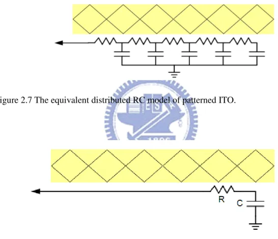
Figure 2.7 The equivalent distributed RC model of patterned ITO. ... 19
Figure 2.8 The equivalent simplified RC model of patterned ITO. ... 19
Figure 2.9 The configuration of surface acoustic wave touch panel [16]. ... 20
Figure 2.10 The configuration of infrared touch panel [17]. ... 21 Figure 3.1 Equivalent model of the capacitive sensor line on a 2.8 inch touch panel. 24 Figure 3.2 Block diagram of the new proposed capacitive touch panel readout circuit
~ x ~
with 4-bit ADC. ... 26
Figure 3.3 Schematic of proposed readout circuit with threshold voltage compensation and its timing chart... 27
Figure 3.4 Simulated results of the proposed readout circuit for capacitive sensor (a) without threshold voltage compensation and (b) with threshold voltage compensation under different threshold voltage. ... 30
Figure 3.5 Simulated results of the proposed readout circuit for capacitive sensor with threshold voltage and mobility (µ0) variation (a) without threshold voltage compensation, and (b) with threshold voltage compensation. ... 31
Figure 3.6 Charge injection effect when a switch turns off. ... 33
Figure 3.7 Clock feedthrough effect when a switch turns off. ... 34
Figure 3.8 Circuit configuration of A/D converter. ... 35
Figure 3.9 The 4 bits on-panel readout circuit of capacitive sensor suitable for LTPS process... 36
Figure 3.10 The simulated result of the proposed circuit under the non-touch event with the digital output code of ‘1111’. ... 37
Figure 3.11 The simulated results of the proposed readout circuit with (a) Ct = 1pF (digital output code: ‘1110’), (b) Ct = 2pF (digital output code: ‘1100’), (c) Ct = 3pF (digital output code: ‘1000’), and (d) Ct > 3pF (digital output code: ‘0000’). ... 38
Figure 3.12 The diagram of panel touched by finger. ... 39
Figure 4.1 The layout view of proposed circuit. ... 41
Figure 4.2 The die photo of the fabricated readout circuit with Indium Tin Oxide (ITO) on glass substrate. ... 42
Figure 4.3 The fabricated circuit on glass substrate to verify the readout function of the proposed circuit. ... 42
Figure 4.4 The fabricated circuits on glass substrate to verify the readout function of the proposed circuit and its corresponding measurement setup. ... 43
Figure 4.5 The measured result of the fabricated circuit under non-touch event (Ct = 0pF) with the output code of ‘1111’. ... 44
Figure 4.6 The measured results of the fabricated readout circuit verified with the Ct of (a) 1pF (digital output code: ‘1110’), (b) 2pF (digital output code: ‘1100’), (c) 3pF (digital output code: ‘1000’), and (d) >3pF (digital output code: ‘0000’). The corresponding digital codes can be successfully generated at the output Vout1, Vout2, Vout3, and Vout4. ... 46
Figure 4.7 The measured result of the fabricated circuit under non-touch event. ... 47
Figure 4.8 The measured results of the fabricated readout circuit under the touched area by finger covered with (a) less than 1/4, (b) 1/2, (c) 3/4, and (d) full of the ITO area. ... 49
Figure A.1 The schematic of clock generator with one input CLK4...52 Figure A.2 The clocks CLK1~CLK6 generated by clock generator...53
~ 1 ~
Chapter 1
Introduction
1.1 Motivation
1.1.1 LCD Industry and LTPS Technology [1], [2]
In recent year, the liquid-crystal display (LCD) industry has attracted much attention in many market areas, e.g. notebook computers, monitors, mobile equipment, mobile telephones, televisions, and so on. For high-speed communication networks, the emerging portable information tools are expected to grow in rapid development of display technologies. Thus, the development of higher specification is demanded for LCD as an information display device. Moreover, the continual growth in network infrastructures will drive the demand for displays in mobile applications and flat panels for computer monitors and TVs. The specifications of these applications will require high-quality displays that are inexpensive, energy-efficient, lightweight, and slim.
In past years, amorphous silicon (a-Si) thin-film transistors (TFTs) are widely used for flat-panel displays. However, the low field-effect mobility (ability to conduct current) limits their application only as pixel switching devices. Therefore, the excimer laser annealing (ELA) process is established for manufacturing of polycrystalline Si (poly-Si) TFTs. The laser annealed polycrystalline silicon has relatively larger grain size. Thus, it exhibits higher carrier mobility (about 100 times) than that of a-Si TFTs. Because of the high driving ability of poly-Si TFTs, it allows the integration of various circuits on panel, for example, integrating the external driving ICs, which are used for driving the pixel, directly onto the peripheral of the glass substrate. It yields a lighter and thinner display with a drastic reduction of
connection pins. It also improves the reliability against the mechanic shock as well as relaxes the limit in the pitch between connection terminals to be suitable for high resolution display. Thus, eliminating LSI (large-scale integration) chips for display drivers will decrease the cost and thickness of displays for various applications. Moreover, high driving ability of poly-Si can provide larger aperture ratio because poly-Si TFTs can drive the same current as a-Si TFTs but only occupy small space.
There are high-temperature and low-temperature poly-Si (HTPS and LTPS) TFTs, defined by the maximum process temperature they can withstand. The process temperature for high-temperature poly-Si can be as high as 900°C. Hence, expensive quartz substrates are required, and the profitable substrate size is limited to around 6 inch (diagonal). Typical applications in such size are limited to small displays. On the other hand, the process temperature for low-temperature poly-Si (LTPS) TFTs is less than 600°C, which would allow the use of low-cost glass substrates. This makes direct-view large-area displays possible—for example, UXGA (ultra extended graphics array) monitors of up to 15.1 inch (diagonal) with a resolution of 1600 x 1200 pixels. For this reason, LTPS technology has been applied successfully to not only small-sized displays, but also medium- and large-screen products. It is the base for high performance TFTs for active matrix liquid crystal displays.
1.1.2 The Advantages of the System-on-Panel LTPS TFT-LCD Displays [4], [5]
Forming a part of display circuits on the glass substrate in LTPS TFT technology has been put into practical use as a compact, high reliable, high resolution display. Because of these properties, LTPS TFT-LCD technology is widely used for mobile displays. Fig. 1.1 shows the system integration roadmap of LTPS TFT-LCD [3].
System-on-Panel (SOP) displays are value-added displays with various functional circuits, including static random access memory (SRAM) in each pixel,
~ 3 ~
integrated on the glass substrate. Fig. 1.2 shows the basic concept of pixel memory technology. When SRAMs and a liquid crystal AC driver are integrated in a pixel area under the reflective pixel electrode, the LCD is driven by only the pixel circuit to display a still image. It means that no charging current to the data line for a still image. This concept is more suitable for ultra low power operation.
Eventually, it may be possible to combine the keyboard, CPU, memory, and display into a single “sheet computer” [7]. The schematic illustration of the “sheet computer” concept and a CPU with an instruction set of 1-4 bytes and an 8-bit data bus on glass substrate are shown in Fig. 1.3, respectively [1], [6]. Fig. 1.4 shows the roadmap of LTPS technologies leading toward the realization of sheet computers. Finally, all of the necessary function will be integrated in LTPS TFT-LCD and the actual operation of 50MHz with 1-µm design will be realized near future [7].
Figure 1.2 Basic concept of pixel memory technology [3].
Figure 1.3 (a) The schematic illustration of the “sheet computer” concept and (b) a CPU with an instruction set of 1-4 bytes and an 8-bit data bus on glass substrate [6].
~ 5 ~
Figure 1.4 The roadmap of LTPS technologies leading toward the realization of sheet computers [7].
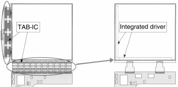
The distinctive feature of the LTPS TFT-LCD is the elimination of TAB-ICs (integrated circuits formed by means of an interconnect technology known as tape-automated bonding). Therefore, the reliability and the yield of the manufacture of high-resolution displays, and more flexibility in the design of the display system, can be further achieved. LTPS TFTs can be used to manufacture complementary-metal-oxide semiconductor (CMOS) devices in the same way as in crystalline silicon-metal-oxide semiconductors field-effect transistors (MOSFETs). Fig. 1.5 shows the cross-sectional structure of p-channel and n-channel TFTs in an LTPS process, where the n-channel TFT has a lightly doped drain (LDD).
Figure 1.5 Schematic cross-section view of the structure of a LTPS complementary metal oxide semiconductor (CMOS). LDD = lightly doped drain.
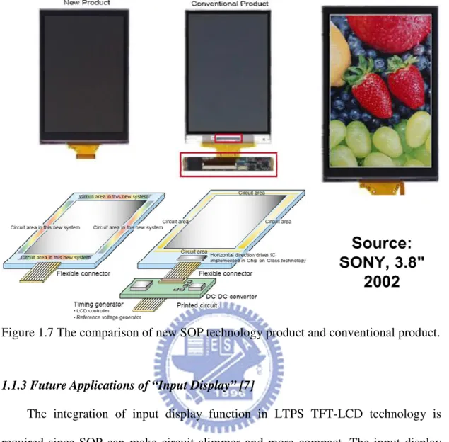
For a-Si TFT-LCDs, TAB-ICs are connected to the left and bottom side as the Y driver and the X driver, respectively. Integration of the Y and X drivers with LTPS TFTs requires PCB (printed circuit board) connections on the bottom of the panel only. The PCB connection pads are thus reduced to one-twentieth the size of those in a-Si TFT-LCDs. The most common failure mechanism of TFT-LCDs, disconnection of the TAB-ICs, is therefore decreased significantly. For this reason, the reliability and yield of the manufacturing can be improved. Decreasing the number of TAB-IC connections also achieves a high-resolution display because the TAB-IC pitch (spacing between connection pads) limits display resolution to 130 ppi (pixels per inch). A higher resolution of up to 200 ppi can be achieved by LTPS TFT-LCDs. Therefore, the SOP technology can effectively relax the limit on the pitch between connection terminals to be suitable for high-resolution display. Furthermore, eliminating TAB-ICs allows more flexibility in the design of the display system because three sides of the display are now free of TAB-ICs [1]. Fig. 1.6 shows a comparison of a-Si and LTPS TFT-LCD modules. The 3.8” SOP LTPS TFT-LCD panel has been manufactured successfully and it is shown in Fig. 1.7.
Figure 1.6 Comparison of (a) an amorphous silicon TFT-LCD module and (b) a low-temperature polycrystalline silicon TFT-LCD module.
~ 7 ~
Figure 1.7 The comparison of new SOP technology product and conventional product.
1.1.3 Future Applications of “Input Display” [7]
The integration of input display function in LTPS TFT-LCD technology is required since SOP can make circuit slimmer and more compact. The input display technology opens opportunities for new applications for personal and business use. The new technology can be applied to diverse products, from cellular phones to personal computers.
The full scope to our imagination concerning future use of “Input Display” is shown in Fig. 1.8. The applications for “Input Display” include recording of text or images for on-line shopping, a scanner device saving personal data and images to a computer, auto-power control with photo-sensor suitable for extremely low power cellular phone, name card reading system, scanner detected by the photo sensor or ambient light sensor to detect the position of finger or pen for some touch-sensing, and so on.
Figure 1.8 Future applications of “Input Display” [7].
1.1.4 Summary
According to above discussion, it can be seen that the integration of the input display function is developed and the fabrication cost will gradually be lowed as SOP will be implemented step by step in the future. Such integration technology contributes to shorten the product lead-time because lengthy development time of ICs can be eliminated. Actually, this integration level has been proceeding from simple digital circuits to the sophisticated ones.
Touch panel is one of the most important “Input Display” applications. It has been implemented on glass substrate for years. However, the relative control ICs are usually fabricated in silicon CMOS technology for its low malfunction and high stability. In this thesis, an on-panel analog readout circuit for capacitive sensor with LTPS technology is proposed. With the integration of ADC in LTPS process, 4-bit
~ 9 ~
resolution can be achieved, i.e. four different sensed capacitance values can be distinguished, to enhance the overall resolution for touch panel by using the interpolation method. The proposed circuit has been designed and realized in a 3-µm LTPS process.
1.2 Background Knowledge of Thin-Film Transistors LCD
1.2.1 Brief Introduction of Liquid Crystal Displays [8], [9]
A liquid crystal display (LCD) is an electronically-modulated optical device shaped into a thin, flat panel made up of any number of color or monochrome pixels filled with liquid crystals and arrayed in front of a light source (backlight) or reflector.
The incident light can be modulated through the liquid crystal as shown in Fig. 1.9. There are two perpendicular polarizer filled with liquid crystal molecule. In general, the first polarizer of a couple of polarizers is called polarizer and the second polarizer of these is called analyzer. The light can be blocked by a couple of polarizers with 90° phase error, is shown in Fig. 1.9 (a). If we twist the liquid crystal molecule by applying the specific electric field across it, the light still can pass the polarizer. This is because the direction of liquid crystal molecules varies with electric field and it can guide the light along the long axis, shown in Fig. 1.9 (b).
Figure 1.9 (a) A couple of polarizers with 90° phase error. (b) A couple of polarizers with liquid crystals [10].
The twisted nematic (TN) device is the most common liquid crystal device and its structure is shown in Fig. 1.10. A structure of TN-LCD consists of a pair of polarizer to block the incident light, a pair of transparent electrode to modulate the liquid crystal molecule phase, and a pair of orientation layer which is also perpendicular to each other so the liquid crystal molecules arrange themselves in a helical structure, or twist.
The optical effect of a twisted nematic device in the voltage-on state is far less dependent on variations in the device thickness than that in the voltage-off state. Therefore, these devices are usually operated between crossed polarizers such that they appear bright with no voltage. These devices can also be operated between parallel polarizers, in which case the bright and dark states are reversed.
Fig. 1.10 (a) shows a pixel of a transmissive twisted nematic LC-cell with no voltage applied. The backlight f passes the polarizer a. The light leaves it linearly in the direction of the lines in the polarizer, and passes the glass substrate b, the transparent electrode c out of Indium-Tin-Oxide (ITO) and the transparent orientation layer g. In this case, the analyzer is crossed with polarizer. The light can pass the analyzer without applied voltage due to the twisted nematic LC-cell and the pixel appears white. If the applied voltage is large enough as shown in Fig. 1.10 (b), the
~ 11 ~
liquid crystal molecules in the center of the layer are almost completely untwisted and the polarization of the incident light is not rotated as it passes through the liquid crystal layer. This light will then be mainly polarized perpendicular to the second filter, and thus be blocked and the pixel will appear black. By controlling the voltage applied across the liquid crystal layer in each pixel, light can be allowed to pass through in varying amounts thus constituting different levels of gray.
This operation is termed the normally white (NW) mode. On the contrary, if the analyzer is rotated by 90°, paralleled with polarizer, the light is blocked in the analyzer. The pixel is black. This is called the normally black (NB) mode.
Figure 1.10 The structure of a TN-LCD (a) while light is passing, and (b) while light is blocked. a: polarizer; b: glass substrate; c: transparent electrode, d: the distance between orientation layers, e: liquid crystal, f: backlight, and g: orientation layer [8].
1.2.2 Liquid Crystal Display Module Structure
The cross section structure of TFT-LCD panel is shown in Fig. 1.11 particularly. It can be roughly divided into two part, TFT array substrate and color filter substrate, by liquid crystal filled in the center of LCD panel. We still need a backlight module including an illuminator and a light guilder since liquid crystal molecule cannot light
by itself. However it usually consumes the most power of the system, some applications such as mobile communications try to exclude or replace it from the system. There consists of a polarizer, a glass substrate, a transparent electrode and an orientation layer in TFT array substrate. In color filter substrate, it is composed of an orientation layer, a transparent electrode, color filters, a glass substrate and a polarizer. Most transparent electrodes are made by ITO, and they can control the directions of liquid crystal molecules in each pixel by voltage supplied from TFT on the glass substrate. Color filters contain three original colors, red, green, and blue (RGB). As the degree of light, named “gray level”, can be well controlled in each pixel covered by color filer, we will get more than million kinds of colors.
Figure 1.11 The cross section structure of TFT-LCD panel.
1.3 Thesis Organization
The overview of touch panel technology is discussed in chapter 2. The concept and simulation results of the proposed readout circuit are discussed in chapter 3. Then, the proposed circuit which is fabricated on the glass substrate in 3-µm LTPS process is measured and discussed in chapter 4. In the last chapter, the conclusions of this thesis and the future work are stated.
~ 13 ~
Chapter 2
Overview of Touch Panel Technology
Because touch panel applications allow user to operate instrument directly, it has been one of the most popular electronic consuming products. In this chapter, several different types of touch panel are introduced.
2.1 Resistive Touch Panels
2.1.1 4-wire Resistive Touch Panels [11], [12]
The structure of 4-wire resistive touch panel consists of two transparent layers coated with a conductive material stacked on top of each other as shown in Fig. 2.1. A dot spacer layer is added to separate the top and bottom layer to avoid a malfunction caused from short circuit current in non-touch situation. When pressure is applied on the screen, the top layer makes contact with lower layer. As shown in Fig. 2.2, the coordinate of touch panel can be distinguished by applying the voltage to one layer first and judge whether it is touched or not by reading the voltage of the other layer. The two resistive lines represent the equivalent model of the top and bottom ITO. The general operation principle of 4-wire resistive touch panel is that the top layer is responsible for reading the x coordinate; on the other hand, the bottom layer is responsible for reading the y coordinate. Two conductive lines are added in the peripheral area of ITO glass and ITO film. A fixed voltage is set to these lines respectively to create a uniform electrical field (normally +5V and 0V). Fig. 2.3 shows the process of reading the coordinate of touching position. At first, the two conductive line of top layer are connected to +5V and 0V respectively. When the panel is touched, according to different touch position, the voltage of bottom layer will be set to different voltage. Depending on the voltage read out from bottom layer,
the touch position on Y axis of panel can be calculated by the formula: * x t y cc V Y L V = , (2.1) where Yt is the touch position on Y axis of panel, Vx is the voltage read out from
bottom layer, Vcc is a fixed voltage connected to the conductive line of top layer, and
Ly is the length of panel.
Following this rule, the touch position on X axis of panel can be obtained by setting the voltage of conductive lines of bottom layer and read out the voltage from top layer. The touch position on X axis of panel can be expressed as:
* y t x cc V X W V = , (2.2) where Xt is the touch position on X axis of panel, Vy is the voltage read out from top
layer, and Wx is the width of panel.
These signals of touch position (Xt,Yt) will be transformed into digital signals by
controller and then transfer this digital information to host to give user a correct response.
~ 15 ~
Figure 2.2 The equivalent model for resistive touch panel in no touch and touch event [12].
Figure 2.3 The reading process of 4-wire touch panel [12].
2.1.2 5-wire Resistive Touch Panels [13]
The basic structure of 5-wire resistive touch panel is similar with 4-wire resistive touch panel. The major difference between them is that 5-wire resistive touch panel only uses one layer (top or bottom) to calculate the touch position and 4-wire resistive touch panel uses one layer to calculate X coordinate and the other one to read Y coordinate. 5-wire resistive type touch panels are generally more durable than 4-wire
resistive type. Although clarity is less than other touch panel types, resistive screens are very durable and can be used in different operating environments.
2.2 Capacitive Touch Panels
2.2.1 Surface Capacitive Touch Panels [14]
Surface capacitive touch panels are made up with a glass layer coated with a uniform conductive material. Compared with resistive type touch panels, using very thin indium tin oxide as the conducting material can achieve higher clarity since it is transparent and colorless. Each side of the touch panel maintains a precisely controlled electron in the horizontal and vertical directions which set up a uniform electric field across the conductive layer. As human fingers or other conductive objects touch the panel, a small transport of charge is from the electric field of the panel to the field of the touching object as shown in Fig. 2.4 and current is drawn from each corner of the panel meanwhile. This process is measured with sensors located in the corners, and a microprocessor interpolates an exact position of the touch object based on the values measured. Panels based on surface capacitive technology can provide a high accuracy to detect position.
~ 17 ~
Figure 2.4 Surface capacitive touch surfaces: touching the panel contributes to a current drawn from each corner [14].
2.2.2 Projected Capacitive Touch Panels [15]
Projected capacitive touch panels detect the changes in sensor capacitance, and then using interpolation method to calculate the exact finger position. Currently, the sensor line layout in diamond shapes for conductive sensors, which are made up with indium tin oxide (ITO) to enhance the sensed touching capacitance. The sensor layout pattern is shown in Fig. 2.5.
The A sensors in Fig. 2.5 are connected vertically and responsible for sensing the X-axis of the touch panel. The B sensors are connected horizontally and responsible for sensing the Y-axis of the touch panel. The circle spot in this figure represents for the finger position. The bars represent the change in capacitance when the touch panel is touched by conductive objects. The length of these bars is directly dependent on the thickness and dielectric of the protective touch panel cover, which affects resolution directly.
Figure 2.5 The configuration of projected capacitive touch panel when in touching event [15].
Figure 2.6 Typical touch panel stack up for projected capacitive touch panel.
Fig. 2.6 shows the typical stack up of touch panel. The air gap helps eliminate radiated noise which is coupled from the LCD since its relative dielectric is about three times less than the adhesive. Additionally, adding the shield layer (sheet ITO) can eliminate noise coupling, reduce most parasitic capacitance, and boost the overall induced capacitance owing to the touch objects. The protective touchscreen cover is
~ 19 ~
typically chosen as high quality optical plastic or glass. This layer impacts the resolution for touch panel applications directly.
The patterned signal ITO panel can be modeled as a lumped distributed series RC line as shown in Fig. 2.7. After the touchscreen XY dimensions are judged, this lumped model can be further simplified into a simple RC circuit which represents the total capacitance and resistance of the touchscreen as shown in Fig. 2.8.
Figure 2.7 The equivalent distributed RC model of patterned ITO.
2.3 Other Touch Panels
2.3.1 Surface Acoustic Wave (SAW) Touch Panels [16]
The configuration of surface acoustic wave touch panel, which uses a substrate to propagate surface acoustic wave, is shown in Fig. 2.9. The acoustic wave signals propagate in the predetermined path. When a touch event happens, it will contribute to amplitude damping on the passing wave. The level of damping is relative to the touch pressure.
Figure 2.9 The configuration of surface acoustic wave touch panel [16].
2.3.2 Infrared (IR) Touch Panels [17]
The infrared touch panels consist of two transmitter and receiver pairs as shown in Fig. 2.10. The transmitter is made up with infrared LED and the receiver consists of photodetector. These two pairs are in charge of detecting X-axis touch position and
~ 21 ~
Y-axis touch position respectively. When objects (conductive or insulating) touch the panel surface, the signal emitted by the transmitter will be blocked off. Depending on whether the signal achieves receiver or not, whether the panel is touched can be known and further know the exact touch position.
Chapter 3
On-Panel Readout Circuit for Capacitive Touch
Panel
3.1 Introduction
Low temperature poly-silicon (LTPS) thin-film transistors (TFTs) have been widely applied in the active-matrix liquid crystal display (AMLCD) to integrate analog and digital circuits on glass. Through LTPS TFTs process, the circuits in CMOS process like driving circuits, analog-to-digital converters (ADC), timing controller etc. on the peripheral area of display can be integrated to glass substrate to achieve slim, compact, and high-resolution display. The characteristics of poly-Si TFT, such as high carrier mobility, low threshold voltage, high stability, and high reliability, are required to fulfill the SOP application [18], [19].
Nowadays, touch panel becomes more and more popular for its simplicity and direct interaction with consumer electronics applications such as satellite navigation devices, mobile phone, personal digital assistants (PDAs), notebook, and so on. Therefore, integrating touch panel into glass substrate has attracted much attention in last few years.
Touch panels utilized in consumer electronics applications are mainly resistive or capacitive. Resistive touch panel delivers cost-effective, consistent and durable performance in environments. Disadvantages of resistive technology include serious glare, low transmittance and single touch only. On the other hand, capacitive touch panel can realize multi-touch functionality easily which allows user to operate information instruments more intuitively [20], [21]. In [22], one on-panel readout circuit for touch panel application has been proposed with minimum detectable
~ 23 ~
voltage difference of the proposed circuit is 30 mV. The switch-capacitor (SC) technique is applied to enlarge the voltage difference from the capacitance change of touch panel and the corrected double-sampling (CDS) technique is also employed to reduce the offset owing to process variation.
However, in LTPS TFTs process, it bases on excimer laser crystallized poly-Si which contributes to random orientation of poly-Si grains, grain size variation, and incomplete termination of grain boundaries. These characteristics usually accompany a random device-to-device threshold voltage variation on panels which result in serious impacts on the accuracy of analog circuits [23], [24].
In this work, a new readout circuit for capacitive sensor on glass has been designed and verified in 3-µm LTPS process [25]. The threshold voltage variation can be compensated by employing switch capacitor technique. A 4-bit analog to digital converter suitable for LTPS process is added to judge different value of sensed capacitance. In this way, the overall resolution for touch panel can be enhanced by interpolation method.
3.2 Circuits Implementation and Simulated Results
3.2.1 Equivalent Model of Capacitive Sensor Line
A capacitive touch panel produced in LTPS process consists of an insulator glass, coated with a transparent conductor indium tin oxide (ITO). When the conductive objects such as finger or metal stylus touch the surface or panel, it will contribute to a small voltage change on the panel surface and can be regarded as a signal to distinguish whether the panel is touched or not. The equivalent model of the capacitive sensor on the 2.8 inch panel line provided by foundry is shown in Fig. 1 with the total resistance of 150kΩ and total capacitance of 100pF. The fanout is the
equivalent parasitic RC of interconnect line between the sensor line to the output node Fin. In order to detect the capacitance change in sensor line, the total sensor line is pre-charged to the supply voltage (VDDA). When the conductive objects touch the surface of touch panel, an additional touch capacitance (Ct) is formed and connected to the equivalent RC circuit. The charge on sensor line will share charge with Ct and results in a voltage variance on the node Fin. After the charge sharing process, the final value of VFin can be expressed as:
Ctotal
VFin VDDA,
Ctotal Ct
= ×
+ (3.1)
where Ctotal = 100pF and VDDA= 15V.
Because the value of Ct is around few pF for different finger touch area, it contributes to a voltage change from ten to hundred mV under VDDA=15V on the total sensor line. The readout circuit is needed to amplify the signal for the process of following stages. Furthermore, the value of Ct is dependent on the distance between
~ 25 ~
touch position and sensor line. Since different Ct leads to different VFin, if the value of Ct can be known, interpolation method can be applied to calculate the touch position when the conductive object touches the position between two sensor lines. The proposed readout circuit with 4-bit ADC can distinguish the difference between Ct and further enhances the overall resolution for touch panel.
In LTPS TFTs process, it bases on excimer laser crystallized poly-Si which contributes to random orientation of poly-Si grains, grain size variation, and incomplete termination of grain boundaries. These characteristics usually accompany a random device-to-device threshold voltage variation on panels which result in serious impacts on the accuracy of analog circuits [23], [24].
The threshold voltage variation impacts have been investigated in many aspects. In [23], this paper investigates the threshold voltage variation effect on output buffer. Without accurate threshold voltage, the common-mode of output voltage may change in a large-scale and further impact the operation of following stage.
Besides, [24] shows the impact of threshold voltage variation on gate-bias. If the threshold voltage may vary, the generated current will be different between TFTs even if the gate-bias is the same. Therefore, a threshold voltage compensation skill is needed to avoid these serious impacts on analog circuit.
3.2.2 Design of On-Panel Readout Circuit and Simulated Results
To compensate the impact of threshold voltage variation, a new readout circuit of capacitive sensor suitable for LTPS process has been proposed. The block diagram of the new proposed readout circuit is shown in Fig. 3.2 which consists of a transconductance amplifier, current integrator and a 4-bit ADC [26].
In the first stage, the input voltage is transformed into the current Iint which equals to VFin×Gm by the transconductance amplifier (Gm amplifier). Secondly, the
current Iint is converted into voltage Vo by charging the current integrator. The Vo can be expressed as:
int
Vo=
∫
K∗I dt, (3.2)where K is a constant.
Since Iint is a function dependent on VFin and Vo is proportional to the integration of current Iint, from the equation above, the input signal will be amplified as time goes by. In addition, with 4-bit ADC, the proposed circuit can judge the different VFin caused by different touch position.
Figure 3.2 Block diagram of the new proposed capacitive touch panel readout circuit with 4-bit ADC.
~ 27 ~
Figure 3.3 Schematic of proposed readout circuit with threshold voltage compensation and its timing chart.
Fig. 3.3 shows the new proposed capacitive touch panel readout circuit with its timing chart. The circuit consists of five pTFT devices, one nTFT device and a loading capacitance Cout. M1~M5 are switches and M6 is in the charge of transconducting voltage into current as a Gm amplifier. The timing chart consists of three periods: (1) compensation period, (2) reset period, and (3) amplification period. In the compensation period, M2, M3, M5, and M6 are switched on. The node Va is charged by the supply voltage VDDA until M6 is in cut-off region. The voltage difference between the source and gate of M6 equals to the threshold voltage of M6 (Vth6). In the meanwhile, the node Vc is set to the supply voltage VDDA. The voltage difference between node Va and Vc is stored on capacitor C1. In the reset period, M2 and M5 are switched off as well as M1 is switched on. Therefore, the
output voltage Vo is discharged to ground by M1 and the node Va maintains the same voltage (VDDA-|Vth6|). During the amplification period, the node Fin is connected to node Vc, dropping a voltage (∆V) which equals to the voltage difference between VDDA and VFin. Because of the charge conservation at the node Va, the voltage of node Va also drops ∆V and becomes equal to (VFin-|Vth6|). In addition, node Va should be discharged to ground in every cycle to guarantee that VDD-|Vth6| can be stored at the node Va successfully. If node Va is initially larger than VDDA-|Vth6|, the compensation operation doesn’t work because M6 turns off. The basic current formula of TFT device can be expressed as following equation:
(
)
2 0 | | | | 2L Cox VGS Vth W I = µ − , (3.3)where µ0 is the carrier mobility, L denotes the effective channel length, W is the
effective channel width, Cox is the gate oxide capacitance per unit area, Vth is the threshold voltage of TFT device. The current of M6 in the amplification period is shown in equation (4):
(
)
2 6 0 2 M ox W I C VDDA VFin Lµ = − , (3.4)This current is not relevant to the threshold voltage of TFT device. Using the compensated current charges the loading capacitor Cout which can be regarded as current integrator, the impact of threshold voltage variation on the output voltage Vo can be reduced as shown in Fig. 3.4. Because the range of threshold voltage variation cannot be provided by the foundry, the ±50% threshold voltage variation is applied according to [27], [28] in Fig. 3.4. The output voltages Vo for proposed circuit with
~ 29 ~
threshold voltage compensation are almost the same. Compared to the readout circuit without threshold voltage compensation, the current Iint variation in amplification period can be reduced from 3120% to 29.3%. In additional to the threshold voltage variation, ±50% mobility variation is also simulated in the proposed circuit in Fig. 3.5. The output voltages Vo of proposed circuit with mobility variation shows larger variation compared with that in Fig. 3.4 and the current Iint variation in amplification period can reduced from 3550% to 33%.
(a)
(b)
Figure 3.4 Simulated results of the proposed readout circuit for capacitive sensor (a) without threshold voltage compensation and (b) with threshold voltage compensation under different threshold voltage.
~ 31 ~
(a)
(b)
Figure 3.5 Simulated results of the proposed readout circuit for capacitive sensor with threshold voltage and mobility (µ0) variation (a) without threshold voltage
3.2.3 Switch Design
In the proposed circuit, many switches are used to control the circuit operation. The detail design is considered in this subchapter. Charge injection and clock feedthrough effects are discussed.
Charge Injection [31]
The conduction of MOS is based on the existence of a channel. When the gate of MOS is biased at an appropriate voltage, for NMOS, many electrons (or holes for PMOS) are attracted to the oxide-silicon surface and the channel is formed to conduct the current from the source to drain. The effect of charge injection is shown in Fig. 3.6. Assuming Vin≈Vout, the total charge Qch in the inversion layer can be expressed as:
(
DD in th)
ch ox
Q =WLC V −V −V , (3.5)
where W represents the width of MOS devise, L denotes the effective channel length, Cox is the gate oxide capacitance per unit area, and VDD is the voltage level when clock is ‘1’. When the MOS switch is turned off, half of the charge will inject to both the source and drain terminal contribute to an error voltage equals:
( ) ox DD in th ci H WLC V V V V C − − ∆ = 2 , (3.6)
where the CH represents the output capacitance.
However, in real circuit, this charge which injects to the source and drain terminal is not exact half of the channel charge. It depends on the impedance of both sides. If the impedance of one side is approximately infinite, total channel charge will
~ 33 ~
flow to the other side.
Figure 3.6 Charge injection effect when a switch turns off.
Clock Feedthrough [31]
In additional to the error caused from charge injection, the MOS switch couples the gate clock through the gate-drain and gate-source overlap capacitance and further contribute to an another type error term. As shown in Fig. 3.7, this error can be expressed as: ov cf CK ov H WC V V WC C ∆ = + , (3.7)
where Cov is the overlap capacitance per unit length.
This kind of error can be viewed as a constant offset if Cov is constant. Because it
is independent of input level, post-calibration can be applied to cancel this offset perfectly. Besides, clock feedthrough is a trade-off between speed and precision. The response time of touch panel is in millisecond order which is a slow process. Hence, the clock feedthrough effect is not obvious in circuit of touch panel.
Figure 3.7 Clock feedthrough effect when a switch turns off.
Based on the formula mentioned above, both errors are proportional to the length and width of MOS switch. Therefore, in the proposed circuit, the switch is designed with the minimum width 3µm and minimum length 3µm. Although the smaller size of MOS devices will result in slower operation speed for circuit, the demand for touch panel response time is between tens Hz which is not a quite high value.
~ 35 ~
Figure 3.8 Circuit configuration of A/D converter.
Fig. 3.8 shows the configuration of ADC suitable for LTPS technology [29], [30]. Again, the switch capacitor technique is applied to cancel the influence of threshold voltage variation of TFT device. All switches are controlled by the clock signals CLK5 or CLK6. The circuit operation has two steps, (1) storing the logic threshold voltage Vth,log on capacitor and (2) compensating Vth,log and comparing Vo with the reference voltage. At first, CLK6 is set to high and the difference between logic threshold voltage Vth,log of inverter and Vref is stored on the capacitor C2. In the comparison period, CLK6 is switched to low and CLK5 is set to high. Due to charge conservation, the input voltage of inverter becomes (Vo+Vth,log-Vref). Two inverter stages as buffer are added to guarantee full-swing of the output voltage.
Furthermore, this circuit also has immunity from threshold voltage variation since the Vth,log is cancelled by storing itself on C2. Four-bit resolution is achieved by using four same ADC structure with different reference voltages Vref1~Vref4 as shown in Fig. 3.9. Fig. 3.10 shows the simulated result of the proposed circuit under the non-touch event with the digital output code of ‘1111’. Fig. 3.11 shows the
simulated results of the proposed readout circuit under different Ct. The digital code of ADC presents ‘1110,’ ‘1100,’ ‘1000,’ and ‘0000’ under Ct = 1pF, 2pF, 3pF, and >3pF, respectively. Depending on the digital bits of Vout, different touch position between two sensor lines can be judged by interpolation method and the overall resolution for touch panel can be enhanced.
Figure 3.9 The 4 bits on-panel readout circuit of capacitive sensor suitable for LTPS process.
~ 37 ~
Figure 3.10 The simulated result of the proposed circuit under the non-touch event with the digital output code of ‘1111’.
The number of sensor lines on panel is limited. If the readout circuit can only distinguish whether the panel is touched or not, when the area between two sensors lines is touched, this kind of circuit cannot judge the correct position but choose one sensor line as the touched side. If the readout circuit can distinguish the different capacitance value due to different touch area, the interpolation method can be utilized to identify the more accurate position without more sensor lines and further to enhance the resolution for touch panel applications. The method for extracting touch position has been shown in Fig. 3.12. As shown in Fig. 3.12, when the touch position is between two sensor lines, the approximate touch position can be calculated by the equation: 1 = + + a t Y a b C Y Y W C C , (3.8)
the induced capacitance between touch object and sensor line, and WY is the distance
between two sensor lines. Since Ca and Cb can be judged by digital codes, more
output bits from ADC can gain the higher resolution for touch panel applications.
(a) (b)
(c) (d)
Figure 3.11 The simulated results of the proposed readout circuit with (a) Ct = 1pF (digital output code: ‘1110’), (b) Ct = 2pF (digital output code: ‘1100’), (c) Ct = 3pF (digital output code: ‘1000’), and (d) Ct > 3pF (digital output code: ‘0000’).
~ 39 ~
Figure 3.12 The diagram of panel touched by finger.
3.3 Summary
An on-panel readout circuit for capacitive sensor has been designed and simulated. Using the proposed threshold voltage compensation technique, the output current can be reduced from 3120% to 29.3%. With 4 bits ADC, 4 different capacitances can be sensed. The interpolation method can be utilized to enhance the resolution for touch panel applications.
Chapter 4
Measured Results of On-Panel Readout Circuit
for Capacitive Touch Panel
4.1 Measurement Setup
The new proposed circuits have been designed and fabricated in a 3-µm LTPS technology. The layout view of proposed circuit has been shown in Fig 4.1. Fig. 4.2 shows the die photo of the fabricated readout circuit with Indium Tin Oxide (ITO) on glass substrate, where the ITO is utilized to verified the sensor line. When the finger touches the ITO, the touched area between ITO and finger results in capacitance change on the sensor line. The larger area is touched the larger capacitance change on the sensor line. The ITO is drawn with the equivalent resistance of 150 kΩ in the square form instead of a line in Fig. 4.2 due to the limitation of layout area in the experimental chip. The area of ITO is 1020 µm x 2770 µm and the area of on-panel readout circuit with threshold voltage compensation is 515 µm x 930 µm. Fig. 4.3 shows the fabricated circuit on glass substrate to verify the readout function of the proposed circuit, when the ITO on the glass substrate is touched by a finger. The 4-bit digital output code is utilized to identify the different touch area and to enhance the resolution of the touch panel. The measurement setup is shown in Fig. 4.4, where the touch capacitance Ct is measured by precision LCR meter of Agilent 4284A, CLK1 to CLK6 are given by Keithley 4200 dual pulse generator, power supply is GPS 4303 DC power supply and the output waveforms are observed by SDO603A oscilloscope. The touch capacitance (Ct) is measured by Agilent 4284A. Through connecting the two ports of one stand-alone ITO, which is especially designed to be touched for capacitance measurement with this instrument, the change of capacitance of ITO can
~ 41 ~
be detected. Therefore, the touch capacitance value with different touch area can be also detected.
Figure 4.2 The die photo of the fabricated readout circuit with Indium Tin Oxide (ITO) on glass substrate.
Figure 4.3 The fabricated circuit on glass substrate to verify the readout function of the proposed circuit.
~ 43 ~
Figure 4.4 The fabricated circuits on glass substrate to verify the readout function of the proposed circuit and its corresponding measurement setup.
4.2 Measured Results
The fabricated readout circuit is first verified with the externally applied input signals (VFin). Fig. 4.5 shows the measured result of the fabricated circuit under non-touch event (Ct = 0pF), where the digital output code is ‘1111.’ Fig. 4.6 shows the measured results of the fabricated circuit under different Ct. The digital output code shows ‘1110,’ ‘1100,’ ‘1000,’ and ‘0000’ under Ct = 1pF, 2pF, 3pF, and >3pF, respectively.
Figure 4.5 The measured result of the fabricated circuit under non-touch event (Ct = 0pF) with the output code of ‘1111’.
~ 45 ~
(b)
(d)
Figure 4.6 The measured results of the fabricated readout circuit verified with the Ct of (a) 1pF (digital output code: ‘1110’), (b) 2pF (digital output code: ‘1100’), (c) 3pF (digital output code: ‘1000’), and (d) >3pF (digital output code: ‘0000’). The corresponding digital codes can be successfully generated at the output Vout1, Vout2, Vout3, and Vout4.
After the successful verification of readout function, the fabricated chip is measured by the different touch area of the finger with a 100-pF capacitor connected to the VFin node, which is used to simulate the touching event modeled in Fig. 3.1. The different digital output codes are confirmed according to the different touch area of ITO. Fig. 4.7 shows the measured result of the fabricated circuit under non-touch event, where the digital output code is ‘1111.’ Fig. 4.8 shows the measured results of the fabricated circuit under different touch area. The digital output code shows ‘1110,’ ‘1100,’ ‘1000,’ and ‘0000’ when the touched area by finger is covered with less than
~ 47 ~
1/4, 1/2, 3/4, and full of the ITO area, respectively. By further analyzing the 4-bit digital codes, the corresponding functions, such as zoom in, zoom out, move, and so on, can be performed on the touch panel by the appropriate algorithm of software in the system.
(a)
~ 49 ~
(c)
(d)
Figure 4.8 The measured results of the fabricated readout circuit under the touched area by finger covered with (a) less than 1/4, (b) 1/2, (c) 3/4, and (d) full of the ITO area.
Chapter 5
Conclusions and Future Works
5.1 Conclusions
A readout circuit for capacitive sensor on glass substrate for panel application has been successfully designed and fabricated in a 3-µm LTPS technology. The switch capacitor technique is applied to enlarge the input signal and eliminates the influence of threshold voltage variation successfully. This new proposed circuit architecture can not only distinguish the panel is touched or not, but also distinguish different value of touch capacitance and further know the touch position between sensor lines by utilizing interpolation method. In additional to threshold voltage variation, mobility variation has been successfully verified. The current difference is controlled in a workable region.
5.2 Future Works
Although the proposed circuit has achieved the basic threshold voltage compensation function successfully, the clock number should be further reduced to lessen the circuit design complexity. Besides, this ADC configuration costs much power because when the ADC is in the compensation period, a static current flows through power supply to ground. Although this ADC structure has immunity from threshold voltage variation, when the switch is in transient state, the noise from charge injection or clock feedthrough could trigger the inverter and contributes to malfunction. Therefore, based on these two reasons, another ADC with immunity from threshold voltage variation should be chosen.
~ 51 ~
Furthermore, the noise (like thermal KT/C, and so on) and power domain will contribute to second order effect on the Gm amplifier. It should be further analyzed.
APPENDIX
In the fabricated circuit, the clock generator is not included but external clock is applied. However, for real products, the clock cannot be applied externally but use clock generator to generate all clocks required. Therefore, in the appendix, the clock generator circuit is shown in Fig. A.1. Only one input CLK4 is required to generate remaining clocks. Fig. A.2 shows the simulated results of clock generator. CLK1~CLK6 is generated by this circuit successfully.
~ 53 ~
Figure A.2 The clocks CLK1~CLK6 generated by clock generator. CLK3 CLK1 CLK2 CLK4 CLK5 CLK6
![Figure 1.1 System integration roadmap of LTPS TFT-LCD [3].](https://thumb-ap.123doks.com/thumbv2/9libinfo/8465189.183321/16.892.134.761.506.956/figure-system-integration-roadmap-of-ltps-tft-lcd.webp)
![Figure 1.4 The roadmap of LTPS technologies leading toward the realization of sheet computers [7]](https://thumb-ap.123doks.com/thumbv2/9libinfo/8465189.183321/18.892.139.754.120.396/figure-roadmap-ltps-technologies-leading-realization-sheet-computers.webp)
![Figure 1.8 Future applications of “Input Display” [7].](https://thumb-ap.123doks.com/thumbv2/9libinfo/8465189.183321/21.892.141.731.143.717/figure-future-applications-input-display.webp)
![Figure 2.1 The structure of 4-wire resistive touch panel [11].](https://thumb-ap.123doks.com/thumbv2/9libinfo/8465189.183321/27.892.150.757.483.999/figure-structure-wire-resistive-touch-panel.webp)
![Figure 2.2 The equivalent model for resistive touch panel in no touch and touch event [12]](https://thumb-ap.123doks.com/thumbv2/9libinfo/8465189.183321/28.892.247.645.112.345/figure-equivalent-model-resistive-touch-panel-touch-touch.webp)
![Figure 2.4 Surface capacitive touch surfaces: touching the panel contributes to a current drawn from each corner [14]](https://thumb-ap.123doks.com/thumbv2/9libinfo/8465189.183321/30.892.210.719.130.496/figure-surface-capacitive-surfaces-touching-contributes-current-corner.webp)
![Figure 2.5 The configuration of projected capacitive touch panel when in touching event [15]](https://thumb-ap.123doks.com/thumbv2/9libinfo/8465189.183321/31.892.162.739.117.820/figure-configuration-projected-capacitive-touch-panel-touching-event.webp)