國 立 交 通 大 學
電子工程學系電子研究所
博 士 論 文
碳摻雜製程與高性能多晶矽奈米線薄膜電晶
體之研究
A Study on Carbon Doping Technology and
High-Performance Poly-Si Nanowire TFTs
研 究 生:李 振 銘
指導教授:崔 秉 鉞
中華民國 一○○ 年 十一 月
碳摻雜製程與高性能多晶矽奈米線薄膜電晶體之研究
A Study on Carbon Doping Technology and High-Performance
Poly-Si Nanowire TFTs
研 究 生
: 李振銘 Student : Chen-Ming Lee
指導教授
: 崔秉鉞 Advisor : Bing-Yue Tsui
國立交通大學
電子工程學系
電子研究所
博士論文
A Dissertation
Submitted to Department of Electronics Engineering
and Institute of Electronics
College of Electrical and Computer Engineering
National Chiao Tung University
In Partial Fulfillment of the Requirements
for the Degree of
Doctor of Philosophy
in Electronics Engineering
November 2011
Hsinchu, Taiwan, Republic of China
碳摻雜製程與高性能多晶矽奈米線薄膜電晶體
之研究
研究生:李振銘
指導教授:崔秉鉞
國立交通大學電子工程學系電子研究所
摘要
在本論文中,吾人首先研究碳摻雜製程對於矽化鎳薄膜之熱穩定性、矽化鎳 接觸之n+/p 接面之影響,並利用低溫碳離子佈植技術搭配固態磊晶退火方式,完 成碳化矽薄膜的製作。其次,吾人成功製作出閘極長度僅三十奈米之高性能多晶 矽奈米線薄膜電晶體,藉由元件結構設計,能得到良好的短通道特性與極高的導 通電流值。吾人也探討元件尺寸大小對於多晶矽薄膜電晶體之電流傳導機制的影 響,並用來解釋所觀察到的兩種自我加熱(self-heating)現象。最後在小尺寸多晶 矽奈米線薄膜電晶體上,吾人首次觀察到隨機電報雜訊(random telegraph noise) 現象,並藉由模型推導與高溫測量,證實晶界陷阱也能造成隨機電報雜訊現象。 我們採用電漿浸潤式離子佈植法(plasma immersion ion implantation),將碳 離子植入至矽基材表面,此技術具備高劑量摻雜與低能量植入的優點,但在低能 量與長時間的佈植過程中,同時會沈積類鑽碳膜(diamond-like carbon)在矽基材表面上,阻擋矽化鎳的形成,因此,必須將反應溫度提升至800 °C,才能形成矽
化鎳。另一種離子植入方式為傳統離子佈植法,碳離子植入矽基材表面能改善矽 化鎳薄膜之熱穩定性,特別是高溫下的結塊現象,其改善效率與存在於矽化鎳與
矽介面間的碳原子數量相關,在足夠的碳原子濃度下,矽化鎳薄膜的結塊溫度與 晶相轉換溫度高達850 °C 以上。即使矽化鎳薄膜厚度減薄時,碳摻雜技術仍能有 效提升矽化鎳薄膜之結塊溫度高達300 °C。然而,對於矽化鎳接觸之 n+/p 接面來 說,矽基材表面經過高劑量(5x1015 cm-2)的碳離子佈植與高溫退火後,仍有許多 殘餘缺陷存在於矽基材表面,在矽化鎳反應的過程中,大量的鎳原子能經由這些 缺陷快速擴散並抵達接面空乏區,造成n+/p 接面漏電流增加。 其次,藉由最佳化碳離子佈植與低溫固態磊晶退火製程,我們已經成功製作 出取代位置上的碳原子濃度百分比為1.046 %的碳化矽薄膜。然而,過高的碳原子 濃度會減緩非晶矽區域的固態磊晶再結晶速率,造成不完全的再結晶與磷摻雜物 重新分佈的現象,此兩因素皆會造成再結晶的碳化矽薄膜的片電阻值上升。 整合全包覆式閘極(gate-all-around)、超薄多晶矽奈米線基體與修正型蕭基 能障(modified Schottky barrier)源汲極結構後,成功實現了閘極長度僅三十奈米 的高性能多晶矽奈米線薄膜電晶體,具備良好的轉移曲線特性。碳離子佈植技術 能解決極薄的全矽化鎳源汲極區域發生的結塊現象。我們也探討短通道效應、窄 線寬效應及氨氣電漿處理對於元件直流特性之影響。當進一步採用高介電常數二 氧化鉿來取代傳統二氧化矽閘極氧化層時,高性能多晶矽奈米線薄膜電晶體在低 閘極電壓(2.587 V)與汲極電壓(1 V)操作下,其驅動電流值高達 549 μA/μm, 為已發表過的文獻中最高的驅動電流值。這些實驗結果開啟多晶矽薄膜電晶體應 用於三維積體電路(three-dimensional integrated circuits)的可能性。
我們也發現多晶矽薄膜電晶體中存在不同的電流傳導機制,大尺寸多晶矽薄 膜電晶體的電流傳導機制為熱游離發射,然而,由於晶界效應消失,小尺寸多晶 矽薄膜電晶體的電流傳導機制會轉變成飄移擴散模型。因此,當多晶矽薄膜電晶
體發生自我加熱效應時,大尺寸多晶矽薄膜電晶體的導通電流會增加,但是小尺 寸多晶矽薄膜電晶體的導通電流會下降。 最後,我們分析小尺寸多晶矽奈米線薄膜電晶體的隨機電報雜訊,包含時域 分析與頻域分析。除了氧化層陷阱與介面能態外,我們也推導由晶界陷阱所導致 之載子數目擾動模型,並藉由高溫測量證實晶界陷阱也能造成隨機電報雜訊現 象,未來欲將多晶矽薄膜電晶體實際應用到三維積體電路或是非揮發性記憶體 時,此晶界陷阱導致之隨機電報雜訊必須納入考慮。
A Study on Carbon Doping Technology and
High-Performance Poly-Si Nanowire TFTs
Student: Chen-Ming Lee
Advisor: Dr. Bing-Yue Tsui
Department of Electronics Engineering & Institute of Electronics
National Chiao-Tung University
Abstract
In this dissertation, we studied the impact of the carbon (C) doping technology on the thermal stability of nickel monosilicide (NiSi) and the Ni-silicide-contacted n+/p junction. Moreover, using the low-temperature C ion implantation (I/I) technique followed by solid phase epitaxy (SPE) annealing, silicon-carbon (SiC) layer with high concentration of substitutional carbon could be achieved. Then, we successfully fabricated the high-performance poly-Si nanowire (NW) thin-film transistor (TFT) with a physical gate length (LG) of 30 nm. Good short-channel characteristics and high driving capability could be obtained by structural engineering. Furthermore, we discussed the influence of device geometry on the current transport mechanism. Two self-heating phenomena observed in poly-Si TFTs could be explained by different current transport mechanisms. Finally, we first observed the random telegraph noise (RTN) phenomenon in small-area poly-Si NW TFTs. The RTN phenomenon could also arise from the capture and emission of a carrier by the grain-boundary trap, which was confirmed by model derivation and high-temperature measurements.
We adopted the plasma immersion ion implantation (PIII) technology to implant C ions into the Si substrate surface. PIII has the advantages of high ion fluences and low energy implantation. However, for low energy and long period PIII process, a diamond-like carbon (DLC) film simultaneously deposited on the Si substrate surface and prevented Ni-silicide formation. Therefore, the silicide formation temperature must be raised to 800 °C. Another I/I method used in this study is the conventional C I/I process. Implanting C ions into the Si substrate surface could improve the thermal stability of the NiSi film, especially for the agglomeration phenomenon at high temperatures. The efficiency of improvement is related to the amount of C atoms at the NiSi/Si interface. With sufficient C concentration, the agglomeration and phase transformation temperatures of the NiSi film could be raised to higher than 850 °C. Even if the Ni-silicide film was thin, the C doping technology could still effectively raise the agglomeration temperature of the Ni-silicide film at high as 300 °C. Moreover, For the Ni-silicide-contacted n+/p junction, after high-dose (5x1015 cm-2) C I/I and high-temperature annealing, there were still many residue defects existing in the Si substrate surface. During the formation of Ni silicide, a large number of Ni atoms would rapidly diffuse and arrive at the junction depletion region via these defects, which caused the increase of the n+/p junction leakage current.
We have successfully fabricated the SiC film with substitutional C concentration of 1.046 % by optimizing the C I/I and SPE annealing processes. Nevertheless, excess C concentration retarded the SPE regrowth rate in the amorphous Si region. Therefore, the incomplete recrystallization and phosphorus (P) dopant redistribution phenomena were observed and both resulted in the increase in sheet resistance of the recrystallized SiC film.
poly-Si body, and modified Schottky barrier (MSB) source/drain (S/D) junction, the high-performance poly-Si NW TFT with LG= 30 nm was successfully realized. It had good transfer characteristics. The fully-Ni-silicided S/D was agglomerated owing to the thinner NiSi film, which could be resolved by the C I/I technology. We also discussed the effects of the short channel, narrow width, and ammonia (NH3) plasma treatment on the dc characteristics of the poly-Si NW TFTs. When the silicon dioxide (SiO2) gate dielectric was further replaced by high permittivity (high-κ) hafnium oxide (HfO2), the driving current of the high-performance poly-Si NW TFT biased at low gate and drain voltages (VGS= 2.587 V and VDS= 1 V) was up to 549 μA/μm. This value is the highest among the published literature. These experimental results open the possibility that poly-Si TFTs could be applied in three-dimensional integrated circuits (3D IC).
We also found different current transport mechanisms in poly-Si TFTs. The current transport mechanism in large-area poly-Si TFTs is considered as thermionic emission. However, the current transport mechanism in small-area poly-Si TFTs transformed into the drift-diffusion model owing to the disappearance of the grain-boundary effect. Therefore, as the self-heating effect (SHE) occurs in poly-Si TFTs, the on-state current increases in large-area poly-Si TFTs but decreases in small-area poly-Si TFTs.
Finally, we analyzed the RTN phenomenon in small-area poly-Si TFTs, such as time-domain and frequency-domain analysis. In addition to the gate oxide trap and the interface state, we also derived the carrier number fluctuation model induced by the grain-boundary trap. By high-temperature measurements, we proved that a capture and a release of a carrier by the grain-boundary trap could also cause the RTN phenomenon. As poly-Si TFTs are applied to future 3D IC or 3D nonvolatile memories, the RTN phenomenon induced by the grain-boundary trap should be considered.
誌謝
本論文的完成,首先要感謝我的指導教授 崔秉鉞博士。老師在研究上嚴謹審 慎的態度以及為人處事上剛正不阿的正直個性,都是值得我學習的好榜樣。此外, 老師面對問題的積極態度以及處理問題的邏輯思考方式,都讓我獲益匪淺,當我 遭遇生活上的困難以及研究上的瓶頸時,老師也會適時地給予協助和鼓勵。亦感 謝老師讓我有機會參與新光計畫課輔活動,獲得許多難忘的教學經驗與生活體驗。 其次,我要感謝國立交通大學奈米中心與國家奈米元件實驗室提供良好的實 驗環境,讓實驗得以順利進行。並感謝辛苦的工程師們與技術員們在機台維護與 元件製程上的協助,特別感謝國立交通大學奈米中心的陳明麗小姐、國家奈米元 件實驗室的劉正財、鄭旭君、吳鴻佑、陳俊淇、吳志明、吳大為、鍾昌貴先生以 及陳琇芝、范庭瑋、李春杏、林婉貞、趙子綾、徐台鳳、姚潔宜、簡依玲小姐, 在實驗製程、結果與分析上,提供許多寶貴的建議與意見,你們的熱心幫忙,都 讓我心中感受到滿滿的溫暖。另外非常感謝國立成功大學貴重儀器使用中心的吳 芃妘小姐、行政院原子能委員會核能研究所的蔡文發博士以及漢民科技公司的陳 恆綱博士的大力幫忙,讓碳離子植入製程能夠順利進行。 感謝奈米電子技術實驗室的各位伙伴,志民、季霈、孟漢與明錡學長們,傳 承與分享許多寶貴的實作與數據分析經驗。感謝玉仁、勻珮與旭茹同學們,在碩 士班期間,一起互相勉勵學習。感謝孝瑜、筱函、曉萱、嘉文、正愷、俊凱、瑞 堯、依成、昆武、勃學、子歆、志展、智超、元宏、暄美、婷婷、定業、嶸健、 培宇、璽允、子瑜、炫滋、孫銘鴻、高銘鴻、克勤、茂元、翰奇、泰源、雪君、 國丞、崇德與哲儒學弟妹們,在實驗室有你們的陪伴,讓研究生活增添了許多歡 樂。另外,也要特別感謝我的大學好朋友黃泊韶同學,過去幾年來每週持續陪我一起運動,排解研究上的壓力。 感謝我最愛的家人,父親 李宗柏先生、母親 張雪娥女士、奶奶 李楊留女士, 從小到大無微不至的照顧,大姊 李金嬋、二姐 李詩琳以及哥哥 李振欽,一路上 互相扶持,有你們的鼎力支持,讓我能夠無後顧之憂,順利完成學業。最後,我 要感謝我的女友 王琇瑩,十二年來不離不棄地在我身旁支持我,妳的鼓勵比什麼 都還有用,使我能夠相信自己,排除萬難,順利畢業。最後,感謝女友家人的包 容與關懷,讓我得以完成夢想,謝謝你們。
Content
Abstract (Chinese)………..…...i
Abstract (English)………...…...iv
Content………....…………...…..ix
Table Captions………....………...…..xii
Figure Captions………....………..xiv
Chapter 1
Introduction...11.1 The Development of CMOS Technology...1
1.2 Carbon (C) Doped Ni-Silicide-Contacted Junction ...3
1.3 The Evolution of Poly-Si Nanowire (NW) TFTs ...6
1.4 Thesis Organization ...8
Chapter 2
Thermal Stability and Formation of Nickel Silicide with Carbon Ion Implantation ...242.1 Introduction...24
2.2 Sample Fabrication ...25
2.2.1 The C I/I samples ...25
2.2.2 The C PIII samples...27
2.2.3 Material Analysis ...28
2.3 Results and Discussion ...28
2.3.1 The C I/I samples ...28
2.3.2 The C PIII samples...32
2.4 Conclusions...34
Chapter 3
Electrical Characteristics of Nickel-Silicide-Contacted Junctions with Carbon Ion Implantation ...563.1 Introduction...56
3.2 Junction Fabrication...57
3.3 Results and Discussion ...58
Chapter 4
Formation of Silicon-Carbon Alloys Using Low-Temperature Carbon Ion
Implantation and Solid Phase Epitaxy ...73
4.1 Introduction...73
4.2 Sample Fabrication ...75
4.3 Results and Discussion ...77
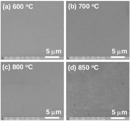
4.3.1 Incomplete Recrystallization and P Redistribution...77
4.3.2 Substitutional C Concentration and Sheet Resistance ...79
4.4 Conclusions...82
Chapter 5
Fabrication and Electrical Characteristics of Gate-All-Around Poly-Si Nanowire Thin-Film Transistors ...995.1 Introduction...99
5.2 Structural Engineering ...101
5.3 Device Fabrication...104
5.4 Results and Discussion ...107
5.4.1 Process Consideration...107
5.4.2 Basic SB and MSB Device Characteristics ...109
5.4.3 Effect of the S/D Series Resistance ...110
5.4.4 Short-Channel and Narrow-Width Characteristics ...113
5.4.5 Temperature-Dependent Transfer Characteristics ...115
5.4.6 Effect of NH3-Plasma Treatment ...117
5.5 Conclusions...118
Chapter 6
Fabrication and Electrical Characteristics of Poly-Si Nanowire Thin-Film Transistors with the High-κ Gate Dielectric...1476.1 Introduction...147
6.2 Device Fabrication...149
6.3 Results and Discussion ...151
6.3.1 Basic MSB Device Characteristics ...151
6.3.2 Self-Heating Effect ...153
Chapter 7
Random Telegraph Noise in Small-Area Poly-Si Nanowire Thin-Film Transistors.176
7.1 Introduction...176
7.2 Results and Discussion ...178
7.2.1 Two-Level ID-RTN ...178
7.2.2 Complex ID-RTN ...181
7.2.3 Carrier Number Fluctuation Model ...182
7.3 Conclusions...186
Chapter 8
Conclusions and Future Recommendations...2038.1 Conclusions...203
Table Captions
Chapter 1
Table 1-1 Doping process technology requirements reported by the 2010 ITRS update for bulk microprocessor unit (MPU) [9]. ...21 Table 1-2 Utility of the substitutional C atom, the interstitial C atom, and C/I clusters in Si. ...22
Chapter 2
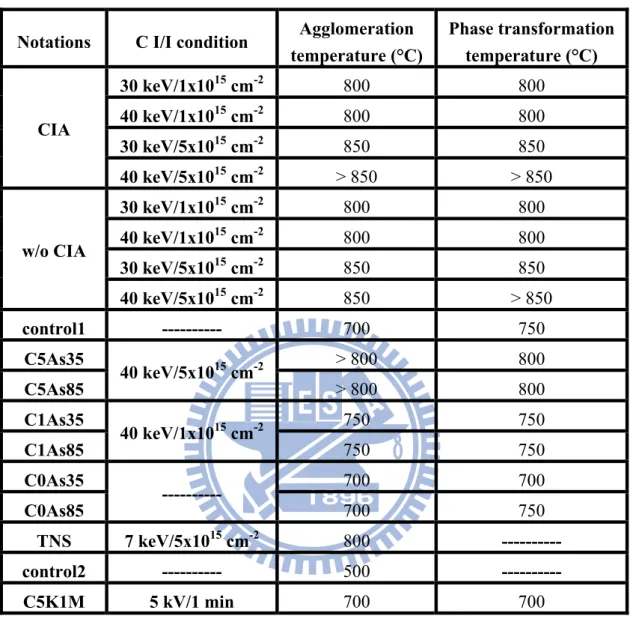
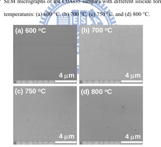
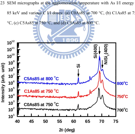
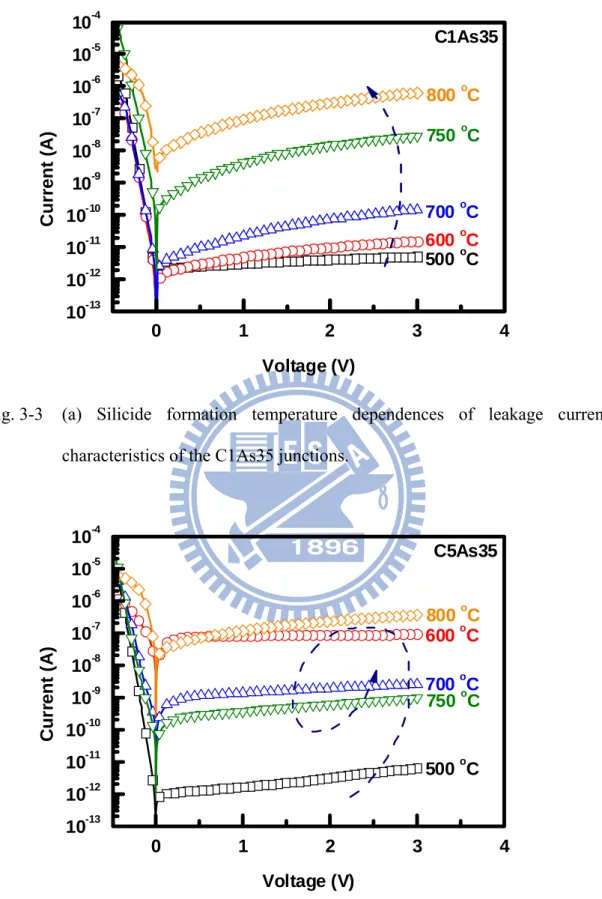
Table 2-1 Summary of substrate types, experimental splits, and their corresponding notations...39 Table 2-2 Summary of the agglomeration and phase transformation temperatures of all samples...40
Chapter 3
Table 3-1 Notations and fabrication conditions of the Ni-silicide-contacted Schottky and n+/p shallow junctions. ...67
Chapter 4
Table 4-1 Comparison of two fabricating methods of SiC S/D stressors. ...88 Table 4-2 Summary of the Rs (Ω/□) values of the RTA-annealed and furnace-annealed samples with different implantation energies, doses, temperatures, and annealing conditions...89 Table 4-3 Summary of the Rs (Ω/□) values of the PLA-annealed samples with different laser energy densities and number of incident laser pulses. Before PLA annealing, these samples were implanted with C (9 keV/5x1015 cm-2 at -15 °C) and P (17 keV/5x1015 cm-2) ions...90
Chapter 5
Table 5-1 Summary of main device parameters of the state-of-the-art high-performance poly-Si TFTs. ...125 Table 5-2 Comparison of various crystallization techniques. ...126
Chapter 6
Table 6-1 Comparison of three n-type MSB poly-Si TFTs. ...162
Chapter 7
Table 7-1 Key parameters of all devices biased at VDS= 1 V. All devices have the same gate oxide thickness of 25 nm and poly-Si channel thickness of 8 nm. ...191
Figure Captions
Chapter 1
Fig. 1-1 Future evolution of the MOSFET including device structures and materials [6]. Where PD SOI and FD SOI represent partially depleted silicon-on-insulator and fully depleted silicon-on-insulator, respectively. MuGFET and MuCFET are the abbreviation for multi-gate FET and multi-channel FET, respectively...23
Chapter 2
Fig. 2-1 Rs values of the CIA samples and control1 samples as a function of annealing temperaure for 30 sec...41 Fig. 2-2 Plan-view SEM micrographs of the CIA samples implanted at 40 keV with a dose of 1x1015 cm-2: (a) 600 °C, (b) 700°C, (c) 800°C, and (d) 850°C...41 Fig. 2-3 XRD spectra of the CIA samples implanted at 40 keV with a dose of 1x1015 cm-2. The silicide formation temperatures are labeled in the figure. ...42 Fig. 2-4 SEM micrographs of the CIA samples implanted at 40 keV with a dose of 5x1015 cm-2 with different silicide formation temperatures: (a) 600 °C, (b) 700°C, (c) 800°C, and (d) 850°C. ...42 Fig. 2-5 XRD spectra of the CIA samples implanted at 40 keV with a dose of 5x1015 cm-2. The silicide formation temperatures are labeled in the figure. ...43 Fig. 2-6 Cross-sectional TEM image of the CIA sample implanted at 40 keV with a dose of 5x1015 cm-2 after silicide formation at 500 °C for 30 sec...43 Fig. 2-7 SIMS depth profile of the CIA sample implanted at 40 keV with a dose of 5x1015 cm-2 after silicide formation at 500 °C for 30 sec. ...44 Fig. 2-8 Rs values of the w/o CIA samples as a function of annealing temperaure for 30 sec. ...44 Fig. 2-9 SEM micrographs of the w/o CIA samples implanted at 30 keV with a dose of 1x1015 cm-2 with different silicide formation temperatures: (a) 700 °C, (b) 800°C, and (c) 850°C. ...45 Fig. 2-10 XRD spectra of the w/o CIA samples implanted at 30 keV with a dose of 1x1015 cm-2. The silicide formation temperatures are labeled in the figure...45 Fig. 2-11 SEM micrographs of the w/o CIA samples implanted at 30 keV with a dose of 5x1015 cm-2 with different silicide formation temperatures: (a) 600 °C, (b) 700°C, (c) 800°C, and (d) 850°C...46 Fig. 2-12 XRD spectra of the w/o CIA samples implanted at 30 keV with a dose of 5x1015 cm-2. The silicide formation temperatures are labeled in the figure...46
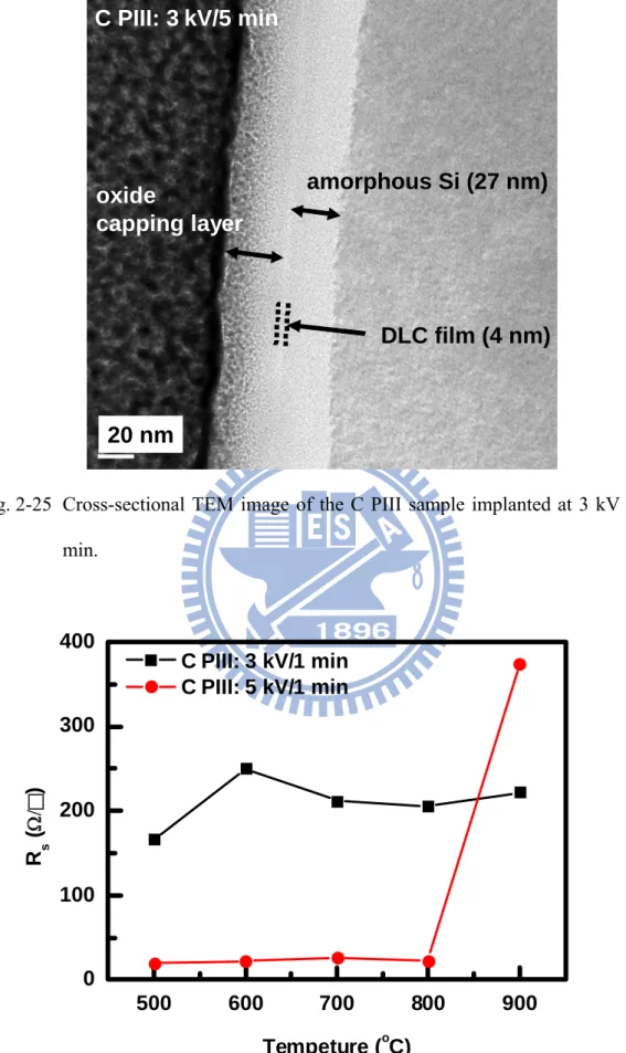
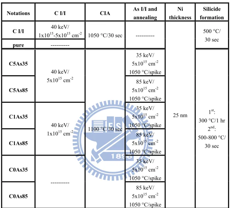
Fig. 2-13 Rs values of the TNS samples and control2 samples as a function of annealing temperaure for 30 sec. ...47 Fig. 2-14 SEM micrographs of the TNS samples implanted at 7 keV with a dose of 5x1015 cm-2 with different silicide formation temperatures: (a) 500 °C, (b) 600°C, (c) 700°C, (d) 800°C, and (e) 850°C...47 Fig. 2-15 SEM micrographs of the control2 samples with different silicide formation temperatures: (a) 500 °C, (b) 600°C, (c) 700°C, (d) 800°C, and (e) 850°C. ...48 Fig. 2-16 Rs values as a function of silicide formation temperature with As I/I energy at 35 keV and different C I/I doses. ...48 Fig. 2-17 SEM micrographs of the C0As35 samples with different silicide formation temperatures: (a) 600 °C, (b) 700 °C, (c) 750 °C, and (d) 800 °C...49 Fig. 2-18 SEM micrographs of the C1As35 samples with different silicide formation temperatures: (a) 600 °C, (b) 700 °C, (c) 750 °C, and (d) 800 °C...49 Fig. 2-19 SEM micrographs of the C5As35 samples with different silicide formation temperatures: (a) 600 °C, (b) 700 °C, (c) 750 °C, and (d) 800 °C...50 Fig. 2-20 XRD spectra of the C1As35 samples. The silicide formation temperatures are labeled in the figure...50 Fig. 2-21 XRD spectra of the C5As35 samples. The silicide formation temperatures are labeled in the figure...51 Fig. 2-22 Rs values as a function of silicide formation temperature with As I/I energy at 85 keV and different C I/I doses. ...51 Fig. 2-23 SEM micrographs at the agglomeration temperature with As I/I energy at 85 keV and various C I/I doses: (a) C0As85 at 700 °C, (b) C1As85 at 750 °C, (c) C5As85 at 750 °C, and (d) C5As85 at 800 °C...52 Fig. 2-24 XRD spectra at the phase transformation temperature with As I/I energy at 85 keV and various C I/I doses...52 Fig. 2-25 Cross-sectional TEM image of the C PIII sample implanted at 3 kV for 5 min. ...53 Fig. 2-26 Rs values of the C3K1M and C5K1M samples as a function of annealing temperaure for 30 sec...53 Fig. 2-27 XRD spectra of the C3K1M samples. The silicide formation temperatures are labeled in the figure...54 Fig. 2-28 SEM micrographs of the C3K1M samples with different silicide formation temperatures: (a) 500 °C, (b) 600 °C, (c) 700 °C, (d) 800 °C, and (e) 900 °C. ...54 Fig. 2-29 XRD spectra of the C5K1M samples. The silicide formation temperatures are labeled in the figure...55 Fig. 2-30 SEM micrographs of the C5K1M samples with different silicide formation temperatures: (a) 500 °C, (b) 600 °C, (c) 700 °C, (d) 800 °C, and (e) 900 °C. ...55
Chapter 3
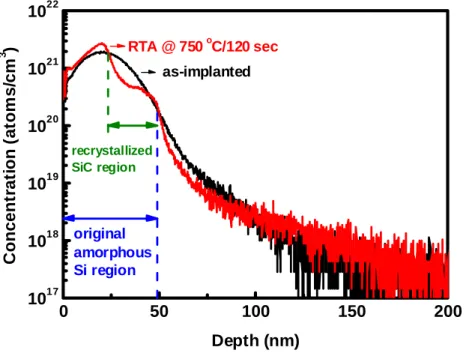
Fig. 3-1 Main process flow of the Ni-silicide-contacted n+/p shallow junction: (a) after LOCOS isolation and screen oxide growth, (b) after C I/I and annealing, (c) after As I/I and activation, and (d) the final structure. ...68 Fig. 3-2 Typical I-V characteristics of the pure and CIA Ni-silicide-contacted Schottky junctions measured at room temperature. Silicide formation is carried out at 500 °C for 30 sec. ...69 Fig. 3-3(a) Silicide formation temperature dependences of leakage current characteristics of the C1As35 junctions...70 Fig. 3-3(b) Silicide formation temperature dependences of leakage current characteristics of the C5As35 junctions...70 Fig. 3-4 Statistics of the reverse-bias junction leakage current at 3 V for the Ni-silicide-contacted n+/p shallow junctions with As I/I at 35 keV. ...71 Fig. 3-5 StatStatistics of the reverse-bias junction leakage current at 3 V for the Ni-silicide-contacted n+/p shallow junctions with As I/I at 85 keV. ...71 Fig. 3-6 SIMS depth profiles of C, Ni, and As of the (a) C5As85 and (b) C0As85 samples with silicide formation temperature at 600 °C...72
Chapter 4
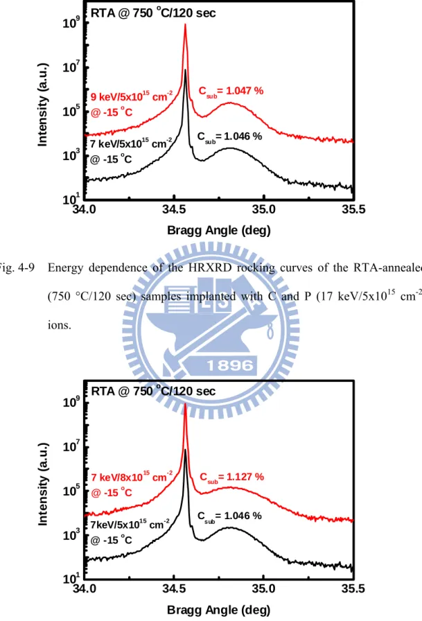
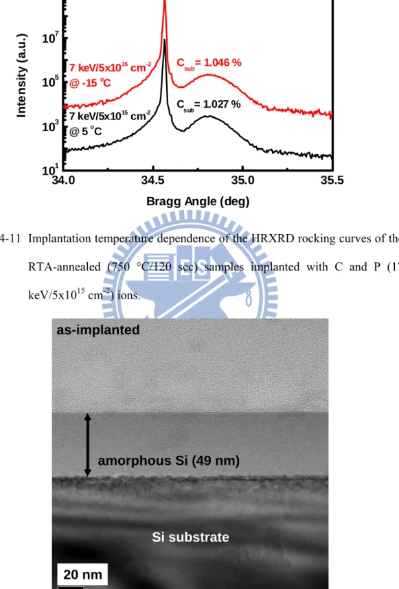
Fig. 4-1 SIMS depth profile of the as-implanted sample implanted with C (7 keV/5x1015 cm-2 at -15 °C) and P (17 keV/5x1015 cm-2) ions. ...91 Fig. 4-2 XTEM image of the as-implanted sample implanted with C (7 keV/5x1015 cm-2 at -15 °C) and P (17 keV/5x1015 cm-2) ions...91 Fig. 4-3 SIMS profile of the RTA-annealed (750 °C/120 sec) sample implanted with C (7 keV/5x1015 cm-2 at -15 °C) and P (17 keV/5x1015 cm-2) ions. ...92 Fig. 4-4 XTEM image of the RTA-annealed (750 °C/120 sec) sample implanted with C (7 keV/5x1015 cm-2 at -15 °C) and P (17 keV/5x1015 cm-2) ions. ...92 Fig. 4-5 XTEM image of the RTA-annealed (750 °C/120 sec) sample implanted only with C (7 keV/5x1015 cm-2 at -15 °C) ions. ...93 Fig. 4-6 XTEM image of the furnace-annealed (750 °C/1 hr) sample implanted with C (7 keV/5x1015 cm-2 at -15 °C) and P (17 keV/5x1015 cm-2) ions. ...93 Fig. 4-7 Comparison of the SIMS profiles of the as-implanted and RTA-annealed (750 °C/120 sec) samples implanted with C (7 keV/5x1015 cm-2 at -15 °C) and P (17 keV/5x1015 cm-2) ions...94 Fig. 4-8 Energy dependence of the HRXRD rocking curves of the RTA-annealed (700 °C/120 sec) samples implanted with C and P (17 keV/5x1015 cm-2) ions...94
Fig. 4-9 Energy dependence of the HRXRD rocking curves of the RTA-annealed (750 °C/120 sec) samples implanted with C and P (17 keV/5x1015 cm-2) ions...95 Fig. 4-10 Dose dependence of the HRXRD rocking curves of the RTA-annealed (750 °C/120 sec) samples implanted with C and P (17 keV/5x1015 cm-2) ions. ...95 Fig. 4-11 Implantation temperature dependence of the HRXRD rocking curves of the RTA-annealed (750 °C/120 sec) samples implanted with C and P (17 keV/5x1015 cm-2) ions...96 Fig. 4-12 XTEM image of the as-implanted sample implanted with C (7 keV/5x1015 cm-2 at 5 °C) and P (17 keV/5x1015 cm-2) ions. ...96 Fig. 4-13 HRXRD spectra of the RTA-annealed samples implanted with C and P (17 keV/5x1015 cm-2) ions after RTA annealing at various temperatures for 120 sec. ...97 Fig. 4-14 HRXRD spectra of the RTA-annealed samples implanted with C and P (17 keV/5x1015 cm-2) ions after RTA annealing at 750 °C for different annealing time...97 Fig. 4-15 HRXRD spectra of the RTA-annealed and furnace-annealed samples implanted with C and P (17 keV/5x1015 cm-2) ions...98 Fig. 4-16 HRXRD spectra of the PLA-annealed samples implanted with C and P (17 keV/5x1015 cm-2) ions...98
Chapter 5
Fig. 5-1 Main process flow of the GAA poly-Si NW TFT integrated with the MSB S/D: (a) after the oxide opening region definition, (b) after the TEOS gate oxide deposition, (c) after a double spacer formation, and (d) the final device structure. ..127 Fig. 5-2 (a) Cross-sectional TEM image of the GAA poly-Si NW TFT along the gate direction with LG/W= 200 nm/35 nm. (b) Enlarged cross-sectional view of (a)...128 Fig. 5-3 (a) Cross-sectional TEM image of the GAA poly-Si NW TFT along the channel direction with LG/W= 30 nm/35 nm. (b) Plan-view TEM of the ultra-thin poly-Si channel. ...129 Fig. 5-4 Top-view SEM image of the active area: (a) after EBL and (b) after the PR ashing process with the ashing time of 40 sec. ...130 Fig. 5-5 Top-view SEM image of the active area after the PR ashing process with the ashing time of 140 sec: (a) LER degradation and (b) the broken line. ...131 Fig. 5-6 Cross-sectional TEM image of the NiSi film at S/D pad regions. ...132 Fig. 5-7 XRD spectra of the NiSi film on SiO2/Si substrate after completing the device fabrication...132 Fig. 5-8 Top-view SEM image of the fabricated poly-Si NW TFT with LG/W= 30 nm/500 nm. ...133
Fig. 5-9 AFM image of the NiSi film at S/D pad regions. ...133 Fig. 5-10 Top-view SEM image of the NiSi film at S/D pad regions implanted with C ions at 1 keV to a dose of 5x1015 cm-2. ...134 Fig. 5-11(a) Transfer characteristics of the smallest SB device with LG/W= 30 nm/35 nm. ...134 Fig. 5-11(b) Output characteristics of the smallest SB device with LG/W= 30 nm/35 nm. ...135 Fig. 5-12(a) Transfer characteristics of the smallest n-type MSB device with LG/W= 30 nm/35 nm. ...135 Fig. 5-12(b) Output characteristics of the smallest n-type MSB device with LG/W= 30 nm/35 nm. ...136
Fig. 5-13 Equivalent circuit diagram of the ELM.
...136 Fig. 5-14 Linear-region transfer characteristics with different external load resistors of the smallest n-type MSB device with LG/W= 30 nm/35 nm. ...137 Fig. 5-15 1/IDS versus RL plot of the smallest n-type MSB device with LG/W= 30 nm/35 nm. ...137 Fig. 5-16 -RL0 versus (VGS-VTH-0.5VDS)-1 plot of the smallest n-type MSB device with LG/W= 30 nm/35 nm...138 Fig. 5-17 Top-view SEM image of the fabricated poly-Si NW TFT with LG/W= 30 nm/35 nm. ...138 Fig. 5-18(a) Statistics of the VTH values of the n-type MSB devices with fixed W= 35 nm and various LG. ...139 Fig. 5-18(b) Statistics of the DIBL values of the n-type MSB devices with fixed W= 35 nm and various LG. ...139 Fig. 5-18(c) Statistics of the ION values of the n-type MSB devices with fixed W= 35 nm and various LG. ...140 Fig. 5-19(a) Statistics of the VTH values of the n-type MSB devices with fixed LG= 30 nm and various W. ...140 Fig. 5-19(b) Statistics of the DIBL values of the n-type MSB devices with fixed LG= 30 nm and various W. ...141 Fig. 5-19(c) Statistics of the ION values of the n-type MSB devices with fixed LG= 30 nm and various W. ...141 Fig. 5-20(a) Temperature-dependent transfer characteristics of the n-type MSB device with LG/W= 5 μm/5 μm...142 Fig. 5-20(b) Temperature-dependent transfer characteristics (linear scale) of the n-type MSB device with LG/W= 5 μm/5 μm biased at VDS= 0.05 V. ...142
Fig. 5-20(c) Temperature-dependent transfer characteristics (linear scale) of the n-type MSB device with LG/W= 5 μm/5 μm biased at VDS= 1 V. ...143 Fig. 5-21(a) Temperature-dependent transfer characteristics of the smallest n-type MSB device with LG/W= 30 nm/35 nm...143 Fig. 5-21(b) Temperature-dependent transfer characteristics (linear scale) of the n-type MSB device with LG/W= 30 nm/35 nm biased at VDS= 0.05 V...144 Fig. 5-21(c) Temperature-dependent transfer characteristics (linear scale) of the n-type MSB device with LG/W= 30 nm/35 nm biased at VDS= 1 V...144 Fig. 5-22 Temperature-dependent transconductance characteristics of the n-type MSB device with LG/W= 30 nm/35 nm biased at VDS= 1 V...145 Fig. 5-23(a) Transfer characteristics of the smallest n-type MSB device with LG/W= 30 nm/35 nm before and after the NH3 plasma passivation...145 Fig. 5-23(b) Typical output characteristics of the NH3-passivated n-type MSB device with LG/W= 30 nm/35 nm...146
Chapter 6
Fig. 6-1 Main process flow of the n-type poly-Si NW TFT combined with the HfO2 gate dielectric: (a) after the active area definition, (b) after the HfO2 deposition, (c) after a double spacer formation, and (d) the final device structure. ...163 Fig. 6-2(a) Cross-sectional TEM image along the channel direction of the n-type poly-Si NW TFT combined with the HfO2 gate dielectric with LG/W= 40 nm/20 nm. ...164 Fig. 6-2(b) Enlarged view of Fig. 6-2(a) showing a-3 nm-thick amorphous interfacial oxide layer between the HfO2 gate dielectric and the poly-Si NW channel...164 Fig. 6-3(a) Cross-sectional TEM image along the gate direction of the n-type poly-Si NW TFT combined with the HfO2 gate dielectric with LG/W= 40 nm/20 nm. ...165 Fig. 6-3(b) Cross-sectional TEM image of the near GAA device with LG/W= 1 μm/200 nm...165 Fig. 6-4 Comparison of the typical non-sintered transfer characteristics of the device A, device B, and device C with LG/W= 5 μm/10 μm. ...166 Fig. 6-5 Plot of ln(IDS/VGS) versus (1/ VGS) and the effective grain-boundary trap density of the device B...166 Fig. 6-6 Non-sintered and sintered transfer characteristics of poly-Si NW TFTs combined with HfO2 gate dielectric, and their LG/W= 90 nm/20 nm...167 Fig. 6-7 Typical sintered transfer and output characteristics of poly-Si NW TFTs combined with HfO2 gate dielectric, and their LG/WG = 40 nm/20 nm...167 Fig. 6-8(a) Connection of pulsed I-V measurements using the WGFMU channel 1 and
WGFMU channel 2...168 Fig. 6-8(b) Timing chart of the pulse waveform with the definition of the pulse parameters...168 Fig. 6-9(a) Example of the monitored voltage waveform as a function of time. The gate bias is a pulsed sweep, and the drain bias is a constant voltage...169 Fig. 6-9(b) Enlarged view of 6-9(a) showing the output waveform corresponds to the user-defined waveform. ...169 Fig. 6-10(a) Gate voltage waveforms monitored by the V monitor and the external probe as a function of time...170 Fig. 6-10(b) Enlarged view of 6-10(a) showing the RC time constant delay of the gate pad can be neglected during pulsed I-V measurements...170 Fig. 6-11(a) Pulsed I-V and dc I-V curves of the n-type bulk MOSFET with LG/W= 75 nm/1 μm...171 Fig. 6-11(b) Pulsed I-V and dc I-V curves of the p-type SOI MOSFET with LG/W= 1 μm/10 μm...171 Fig. 6-12 Pulsed I-V and dc I-V curves of the n-type poly-Si NW TFT with LG/W= 300 nm/1 μm...172 Fig. 6-13 Pulsed I-V and dc I-V curves of the n-type poly-Si NW TFT with LG/W= 30 nm/35 nm. ...172 Fig. 6-14 Pulsed I-V and dc I-V curves of the n-type poly-Si NW TFT with LG/W= 30 nm/120 nm. ...173 Fig. 6-15 Pulsed I-V curves with different pulse width of the n-type poly-Si NW TFT with LG/W= 30 nm/35 nm...173 Fig. 6-16 Pulsed I-V curves with different pulse width of the n-type poly-Si NW TFT with LG/W= 30 nm/120 nm...174 Fig. 6-17 Pulsed I-V and dc I-V curves of the n-type poly-Si NW TFT combined with the HfO2 gate dielectric, and its LG/W is equal to 40 nm/20 nm. ...174 Fig. 6-18 Example of the RTN signal observed in the n-type poly-Si NW TFT with the HfO2 gate dielectric, and its LG/W is equal to 40 nm/20 nm. ...175
Chapter 7
Fig. 7-1 Illustration of electron trapping and detrapping by the oxide trap and interface state. ...192 Fig. 7-2 Example of the two-level ID-RTN observed in the device A. The definition of the capture time (τc), the emission time (τe), and the RTN amplitude (ΔID) are labeled...192 Fig. 7-3(a) Histogram of the time-domain data of the device A biased at VGS-VTH=
-0.43 V and VDS= 1 V. ...193 Fig. 7-3(b) PSD of the device A biased at VGS-VTH= -0.43 V and VDS= 1 V. ...193 Fig. 7-4 ID waveform of the device A with different VGS and a fixed VDS of 1 V. ...194 Fig. 7-5 <τc>, <τe>, and ln(<τc>/<τe>) values of the device A as a function of VGS-VTH. ...194 Fig. 7-6(a) Example of the two-level ID-RTN observed in the device B. ...195 Fig. 7-6(b) PSD of the device B biased at VGS-VTH= 1.26 V and VDS= 1 V. ...195 Fig. 7-7 ID waveform of the device B with different VGS and a fixed VDS of 1 V. ...196 Fig. 7-8 <τc> and <τe> values of the device B as a function of VGS-VTH. ...196 Fig. 7-9 ID waveform of the device C with different VGS and a fixed VDS of 1 V. ...197 Fig. 7-10 ID waveform of the device D with different VGS and a fixed VDS of 1 V. ...197 Fig. 7-11 <τc> and <τe> values of the device C and device D as a function of VGS-VTH. ...198 Fig. 7-12 Examples of the complex ID waveform seen in the device E with different VGS and a fixed VDS of 1 V...198 Fig. 7-13 Histograms of the time-domain data shown in Fig. 7-12. ...199 Fig. 7-14 ID waveform of the device F with different VGS and a fixed VDS of 1 V. ...199 Fig. 7-15 Histograms of the time-domain data shown in Fig. 7-14. ...200 Fig. 7-16 <τc> and <τe> values of the faster trap of the device F as a function of VGS-VTH for the high ID level and low ID level, respectively...200 Fig. 7-17 ΔID values resulting from the faster trap as a function of VGS-VTH at the high ID level and low ID level...201 Fig. 7-18 ΔID/ID values at 300 K and 350 K of the device B as a function of VGS-VTH. ...201 Fig. 7-19 VGS-VTH dependence of the Gm value of the device B at 300 K and 350 K. ...202 Fig. 7-20 Comparison of the ΔID/ID values of some devices as a function of VGS.
Chapter 1
Introduction
1.1 The Development of CMOS Technology
Over the past several decades, CMOS scaling successfully drives the development of the electronic industry. It follows Moore’s law proposed by Gordon Moore in 1965 [1]. Gordon Moore predicted the number of available transistors in the same chip area would be doubled every two years. Device feature size scaling not only reduces production cost and the operating voltage but also increases the operation speed and device density. Therefore, due to these benefits, transistor size has been continuously scaled down to 22 nm in 2011. During the 1965-to-2011 time period, in order to accelerate feature size scaling and sustain Moore’s law, MOSFET structures, materials, and process technologies have changed greatly. First, for solving alignment problems, the aluminum (Al) gate was replaced by the poly-crystalline silicon (poly-Si) gate in the 1970’s [2]. The non-self-aligned gate-last process was changed to the self-aligned gate-first process. Second, the titanium (Ti) self-aligned silicidation (salicide) process was first employed in the early 1990’s to reduce the gate and source/drain (S/D) resistance [3]. Although the silicide material changes from Ti-silicide to cobalt-silicide (Co-silicide) and then nickel-silicide (Ni-silicide), the salicide process is the standard CMOS process flow until now. Third, the strained Si technology was adopted to increase the carrier mobility at the 90-nm technology node in 2003 [4]. Strain engineering can effectively compensate the mobility degradation
caused by high channel doping. Fourth, the high-permittivity (high-κ) gate dielectric/metal gate stack was used to further reduce the equivalent oxide thickness (EOT) at the 45-nm technology node in 2007 [5]. The self-aligned gate-first process was changed to the self-aligned gate-last process because of thermal stability issues associated with the high-κ gate dielectric/metal gate stack. At this time, the MOSFET structure still belonged to the planar bulk structure. Figure 1-1 shows new device structures and materials of the new MOSFET generation predicted by the 2009 International Technology Roadmap for Semiconductors (ITRS) [6].
Although the 2009 ITRS predicted the planar bulk structure can still be used at the 22-nm technology node, on May 4, 2011, Intel Corporation has announced that the three-dimensional (3D) tri-gate transistor structure will go into mass production in the end of 2011 [7]. As compared to the planar bulk structure, the benefits of the tri-gate transistor structure include steeper subthreshold slope, lower leakage currents, and better short-channel effect (SCE) immunity [8]. Therefore, the tri-gate transistor can operate at lower voltage to reduce operating power and improve switching speed. However, according to the 2010 ITRS update, there still remain many difficult challenges to overcome below the 16-nm technology node, such as control of short-channel effects (SCEs) and S/D parasitic series resistance, and continued EOT (< 0.7 nm) and junction depth (~10 nm) scaling [9]. To relax MOSFET scaling issues mentioned above, the concept of 3D integrated circuits (IC) demonstrated as early as in 1979 has been reproposed recently [10]. It is a vertical extension of IC technology and contains the multiple active layers stacked together with vertical interconnections between the layers to achieve 3D on-chip integration. The benefits of 3D IC include improved packing density, reduced total power, and noise immunity [11]. It has been reported that poly-Si thin-film transistors (TFTs) have the potential for extensive
applications in 3D IC [12]. Therefore, the poly-Si-based 3D IC is one of the possible solutions as device feature size scaling faces severe limitations in the future.
1.2 Carbon (C) Doped Ni-Silicide-Contacted Junction
To control SCEs and reduce parasitic S/D resistance, the silicide-contacted junction should simultaneously have ultra-shallow junction depth, low junction leakage, high doping concentration, low sheet resistance (Rs), and low contact resistivity. Their specific requirements in future technology nodes are listed in Table 1-1. Ni monosilicide (NiSi) is used for the contact material in present CMOS technology owing to its several advantages including low resistivity, low contact resistivity, low formation temperature, less Si consumption during silicide formation, line-width independent silicidation, no exhibition of bridging failure, and compatibility with SiGe [3, 13]. However, the major drawback of using NiSi is its poor thermal stability. The NiSi film normally agglomerates at 700 °C and transforms into high-resistive Ni disilicide (NiSi2) phase at 750 °C [14]. Junction depth scaling is accompanied by silicide thickness scaling. The thermal stability of the Ni-silicide film degrades with the thickness reduction, which causes an increase in the Rs values of Ni silicide [15]. For thinner NiSi films, the primary degradation mechanism at a higher temperature is agglomeration [15]. The NiSi film with a thickness of 12 nm on an arsenic (As) doped (100) substrate agglomerates at the temperature as low as 575 °C [15]. Therefore, the thermal degradation of a thin NiSi film becomes a main issue for two-dimensional (2D) IC or 3D IC applications. Although the raised S/D process can relax the thickness scaling issues of Ni silicide [16], it also increases the parasitic capacitance between the gate and S/D electrodes. Furthermore, the contact resistance at the Si/Ni silicide contact interface increases with the decrease in contact area [17].
Therefore, high S/D parasitic series resistance arises from the increased contact resistance and Rs. In recent years, several methods have been studied to reduce the contact resistance [18-20] and to enhance the thermal stability of Ni silicide [21-25].
The impact of the carbon (C) atom on pn junction characteristics has been extensively researched for several years [26-28]. The substitutional C atom (Cs) interacts with Si self-interstitial (I) to form the interstitial C atom (Ci), as shown below [28]:
i s I C
C + → , (1-1) Furthermore, C atoms can also trap Si self-interstitials and then form immobile C/I clusters with higher order complex [26]. The effects of the C atoms and C/I clusters in Si are summarized in Table 1-2. The utility of the C atoms depends on its lattice location. The effect of C/I clusters on the ability to getter gold (Au) and copper (Cu) atoms was first discovered by H. Wong et al. in 1988 [29-30]. Later, H. Wong et al. also found that C atoms in Si can suppress the formation of extrinsic secondary defects after annealing owing to C-interstitial trapping reactions [31]. If secondary defects locate within the depletion region of the pn junction, it leads to an increase of reverse-bias pn junction leakage. Therefore, reduction in the reverse-bias leakage current is achieved by incorporating C atoms into Si [27]. Furthermore, the interstitial trapping characteristics of C atoms imply that they can also reduce interstitial-assisted dopant diffusion in Si. Many experimental results have confirmed that transient enhanced diffusion (TED) of boron (B) and phosphorus (P) is strongly suppressed in C-rich Si [32-34]. Hence, an ultra-shallow pn junction with an abrupt dopant profile can be formed by the retard dopant diffusion in the presence of C atoms. Recently, it has been reported that raising the thermal stability of NiSi is another benefit of the existence of C atoms in Si [25, 35]. Segregation of C atoms at the NiSi grain
boundaries and NiSi/Si interface effectively suppresses the agglomeration of NiSi. Therefore, it is feasible to improve the thermal stability of NiSi with the incorporation of C atoms.
The solid solubility of C in Si is only at concentrations of the order of 1x1017 cm-3 [26], so a small number of the incorporated C atoms are located at the substitutional sites in thermal equilibrium. If a large number of the incorporated C atoms have continued to reside on the substitutional Si lattice site of the S/D junction (~1 % substitutional C atoms in Si) without precipitation after MOSFET fabrication, they can produce uniaxial tensile stress in the Si channel of n-type MOSFETs [36-38]. Hence, using silicon-carbon (SiC or Si1-xCx) S/D stressors provides another way to enhance the electron mobility for future application in state-of-the-art n-type MOSFETs. In addition to several advantages described above, the junction degradation arises from interaction products between C atoms and I [26, 28]. The Ci and C/I clusters create deep-trap energy levels in the Si band gap [26, 39], which causes an increase in the thermal generation leakage current. Furthermore, C/I clusters can also act as neutral scattering centers to reduce the carrier mobility [26]. Therefore, the quantity of the Ci and C/I clusters in the depletion region of a C-doped pn junction should be reduced.
The above brief introduction of the C-doping effects in Si suggests that it is possible to integrate all advantages into the Ni-silicide-contacted pn junction and exclude the disadvantages. The junction characteristics of the C-doped diode with a Ni silicide contact have never been reported before. The C-doping effects on the thermal stability of Ni silicide and their related Schottky and n+/p junction characteristics are both investigated in this thesis. Since it is feasible to integrate SiC
S/D stressors into the C-doped Ni-silicide-contacted n+/p junction, the method of fabricating SiC alloys is also discussed in this thesis.
1.3 The Evolution of Poly-Si Nanowire (NW) TFTs
It is well known that active-matrix liquid crystal displays (AM-LCDs) and an active-matrix organic light emitting diode (AM-OLED) display have been successfully mass-produced with poly-Si TFTs. For high-level applications such as system on panel (SOP) and 3D IC in the future, the characteristics of poly-Si TFTs should be improved to achieve high performance. In the past several years, to achieve this goal, many studies focused on new recrystallization technologies combined with novel device structures. In addition to the conventional solid phase crystallization (SPC) method, large-grain poly-Si films are realized by excimer laser annealing (ELA) or metal-induced lateral crystallization (MILC) [40-43]. The device characteristics exhibit higher performance than the device characteristics of SPC poly-Si TFTs owing to a significant reduction of grain-boundary defects in the poly-Si channel region. Furthermore, the double-gate and tri-gate transistor structures integrated with the poly-Si nanowire (NW) or fin-like channel offer excellent short-channel control. However, the physical gate length (LG) of these high-performance devices is longer than 1 μm.
High-performance SPC poly-Si NW TFTs with multi-gate structures have also been demonstrated recently [44-46]. All of them employed the gate-all-around (GAA) structure to enhance the gate-to-channel controllability and the multiple poly-Si NW channels to raise the current driving capability. H. H. Hsu et al. also reported that device variation of poly-Si NW TFTs can be suppressed by the GAA structure and the multiple poly-Si NW channels [44]. Excellent short-channel behaviors resulting from
the GAA structure and their relative long LG (LG ≧ 0.4 μm) were demonstrated. For future application in the 3D IC technology, similar to conventional MOSFETs, poly-Si TFTs should be scaled down to increase device density. The ultra-short-channel characteristics have been extensively investigated in GAA Si NW MOSFETs [47-50]. K. H. Yeo et al. demonstrated that short-channel immunity of GAA Si NW MOSFETs with LG of 15 nm was achieved [49]. However, the ultra-short-channel characteristics of poly-Si TFTs are seldom reported in the literature. In 2005, B. Y. Tsui et al. first fabricated high-performance poly-Si TFTs with LG as short as 100 nm [51]. Three years later, in 2008, M. Im et al. reported that poly-Si NW TFTs with LG= 20 nm showed poor switching performance [52]. In this thesis, we study the ultra-short-channel characteristics of poly-Si TFTs by structural engineering. The multi-gate structure, ultra-thin poly-Si body, and hafnium dioxide (HfO2) high-κ gate dielectric are employed to obtain good ultra-short-channel characteristics. To lower S/D parasitic resistance, we also fabricate the modified Schottky barrier (MSB) S/D structure via the two-step Ni-salicide process and the implant-to-silicide (ITS) technique [53]. Hence, the high current driving capability is also obtained in this work. Furthermore, the C ion implantation (I/I) technology is used to suppress the agglomeration of the fully-Ni-silicided S/D. These low-temperature fabrication processes are very suitable for 3D IC application.
In addition to the device characteristics, the self-heating phenomenon and noise properties of our high-performance poly-Si TFTs are also discussed in this thesis. The self-heating effect (SHE) resulting Joule heating becomes more and more significant with increasing the current driving capability [54]. The thermal problems of 3D IC are greater than those of 2D IC owing to many dielectric layers [11]. The device is completely surrounded by low thermal conductive inter-layer dielectric (ILD).
Therefore, the device characteristics of high-performance poly-Si TFTs with the high driving capability can be affected by the SHE, which is studied in this thesis.
Low frequency noise (LFN) in large-area poly-Si TFTs has been deeply investigated for several years [55-58]. For small-area poly-Si TFTs, LFN becomes more important because it is inversely proportional to the gate area [59]. The LFN behavior of small-area poly-Si TFTs has never been published. As the device size scales down, random telegraph noise (RTN) can be frequently observed in small-area MOSFETs [60]. RTN has been considered as the origin of LFN and becomes a main issue during device operation. The threshold voltage fluctuation arising form RTN affects the stability of static random access memory (SRAM) and the multi-level cell (MLC) operation of Flash memory [61-62]. In this thesis, we successfully observe the RTN phenomenon in our small-area poly-Si TFTs for the first time. When small-area poly-Si TFTs are applied in 3D IC and 3D stackable TFT Flash memories, RTN should be eliminated by advanced process technology.
1.4 Thesis Organization
In this dissertation, the main research topics can be divided into two parts. The first part contains the C-doping effects on the thermal stability of Ni silicide, the Ni-silicide-contacted junction characteristics, and the formation of SiC alloys. The process technologies and characteristics of GAA poly-Si NW TFTs are discussed in the second part.
In the first chapter of this dissertation, we briefly review the development of CMOS technology. To reduce the S/D series resistance and avoid SCEs, S/D engineering is necessary to achieve low parasitic resistance contacts and the abrupt doping profile. The advantages and disadvantages of the C-doping effects in Si are
also described in detail. The C-doping technology is a promising candidate for the fabrication of the ultra-shallow Ni-silicide-contacted junction. To relax several scaling barriers, 3D IC composed of poly-Si TFTs is one of the possible solutions. Therefore, the evolution of poly-Si NW TFTs is briefly introduced. High-performance poly-Si TFTs with a small device area are needed to build 3D IC. Furthermore, two main issues including the SHE and RTN phenomena in small-area poly-Si TFTs should be resolved in the near future.
In chapter 2, we study the impact of C and dopant atoms on the thermal stability of Ni silicide by using different C I/I technologies. A novel I/I technology, plasma immersion ion implantation (PIII), is used to implant C ions into the Si substrate surface. The thermal stability and formation of Ni silicide are dependent on the implantation and silicide-forming conditions. These experimental results will be discussed in this chapter.
In chapter 3, the influence of C atoms on the Ni-silicide-contacted Schottky and n+/p junctions is discussed in detail. The reverse-bias leakage current mechanism of the C-doped Ni-silicide-contacted Schottky junction is considered as the increased thermionic-field emission. Furthermore, the agglomeration of the Ni-silicide film and the diffusion of Ni atoms into the depletion region result in an increase of the reverse-bias leakage current of the C-doped Ni-silicide-contacted n+/p junction.
In chapter 4, we propose a low-temperature C I/I technology followed by solid phase epitaxy (SPE) regrowth to fabricate SiC alloys. Different SPE annealing technologies are employed to recrystallize the amorphous Si layer. High substitutional C concentration (Csub) can be obtained by process optimization. We find that excess C concentration in Si leads to incomplete recrystallization and P redistribution phenomena.
In chapter 5, we successfully fabricate the smallest GAA poly-Si NW TFT with LG of 30 nm. Good electrical characteristics are demonstrated by structural engineering. The agglomeration of thin Ni-silicide films in the S/D regions can still be improved by the C I/I technology. The difference of current transport mechanisms in large-area and small-area poly-Si TFTs is clarified. The device characteristics can be further improved by using an ammonia (NH3) plasma treatment.
In chapter 6, to reduce the EOT, the HfO2 high-κ gate dielectric is first introduced into poly-Si NW TFTs. Excellent device characteristics can be achieved, especially for high driving capability. Two SHE phenomena related to different current transport mechanisms are observed in large-area and small-area poly-Si TFTs.
In chapter 7, the two-level and complex RTN phenomena can be both observed in our small-area poly-Si NW TFTs for the first time. They can arise from the slow trap or the fast trap. We also derive the carrier number fluctuation model induced by the grain-boundary trap. Model accuracy is determined by high-temperature measurements.
Finally, in chapter 8, we will summarize important conclusions of this thesis. Future works are also suggested in this chapter.
References
[1] G. E. Moore, “Cramming more components onto integrated circuits,” Electronics, vol. 38, no. 8, pp. 114-117, 1965.
[2] R. H. Dennard, F. H. Gaensslen, H. N. Yu, V. L. Rideout, E. Bassous, and A. R. LeBlanc, “Design of ion-implanted MOSFET’s with very small physical dimensions,” IEEE J. Solid-State Circuits, vol. SC-9, no. 5, pp. 256-268, 1974. [3] H. Iwai, T. Ohguro, and S. Ohmi, “NiSi salicide technology for scaled CMOS,”
Microelectron. Eng., vol. 60, no. 1-2, pp. 157-169, 2002.
[4] S. E. Thompson, M. Armstrong, C. Auth, M. Alavi, M. Buehler, R. Chau, S. Cea, T. Ghani, G. Glass, T. Hoffman, C. H. Jan, C. Kenyon, J. Klaus, K. Kuhn, M. Zhiyong, B. McIntyre, K. Mistry, A. Murthy, B. Obradovic, R. Nagisetty, P. Nguyen, S. Sivakumar, R. Shaheed, L. Shifren, B. Tufts, S. Tyagi, M. Bohr, and Y. El-Mansy, “A 90 nm logic technology featuring strained-silicon,” IEEE Trans. Electron Devices, vol. 51, no. 11, pp. 1790-1797, 2004.
[5] C. Auth, A. Cappellani, J. S. Chun, A. Dalis, A. Davis, T. Ghani, G. Glass, T. Glassman, M. Harper, M. Hattendorf, P. Hentges, S. Jaloviar, S. Joshi, J. Klaus, K. Kuhn, D. Lavric, M. Lu, H. Mariappan, K. Mistry, B. Norris, N. Rahhal-orabi, P. Ranade, J. Sandford, L. Shifren, V. Souw, K. Tone, F. Tambwe, A. Thompson, D. Towner, T. Troeger, P. Vandervoorn, C. Wallace, J. Wiedemer, and C. Wiegand, “45 nm high-k + metal gate strain-enhanced transistors,” in VLSI Symp. Tech. Dig., 2008, pp. 128-129.
[6] International Technology Roadmap for Semiconductors, 2009 Edition, Semiconductor Industry Association: San Jose, CA, 2009.
[7] D. Poeter and M. Hachman, “Next Intel Chips Will Have the World’s First ‘3D’ Transistors,” PCMag, May 4, 2011. [Online]. Available: http://www.pcmag.com/article2/0,2817,2384897,00.asp#fbid=Z9bherEqaDt.
[Accessed May 4, 2011].
[8] B. Doyle, S. Datta, M. Doczy, S. Hareland, B. Jin, J. Kavalieros, T. Linton, A. Murthy, R. Rios, and R. Chau, “High performance fully-depleted tri-gate CMOS transistor,” IEEE Electron Device Lett., vol. 24, no. 4, pp. 263-265, 2003.
[9] International Technology Roadmap for Semiconductors, 2010 Edition, Semiconductor Industry Association: San Jose, CA, 2010.
[10] M. W. Geis, D. C. Flanders, D. A. Antoniadis, and H. I. Smith, “Crystalline silicon on insulators by graphoepitaxy,” in IEDM Tech. Dig., 1979, pp. 210-212. [11] A. W. Topol, D. C. La Tulipe, Jr., L. Shi, D. J. Frank, K. Bernstein, S. E. Steen,
A. Kumar, G. U. Singco, A. M. Young, K. W. Guarini, and M. Ieong, “Three-dimensional integrated circuits,” IBM J. Res. Develop., vol. 50, no. 4-5, pp. 491-506, 2006.
[12] K. C. Saraswat, K. Banerjee, A. R. Joshi, P. Kalavade, P. Kapur, and S. J. Souri, “3-D ICs: Motivation, performance analysis, and technology,” in Proc. Eur. Solid-State Circuits Conf., 2000, pp. 406-414.
[13] Q. Xiang, J. S. Goo, J. Pan, B. Yu, S. Ahmed, J. Zhang, and M. R. Lin, “Strained silicon NMOS with nickel-silicide metal gate,” in Symp. VLSI Tech. Dig., 2003, pp. 101-102.
[14] F. F. Zhao, J. Z. Zheng, Z. X. Shen, T. Osipowicz, W. Z. Gao, and L. H. Chan, “Thermal stability study of NiSi and NiSi2 thin films,” Microelectron. Eng., vol. 71, no. 1, pp. 104-111, 2004.
[15] O. Chamirian, J. A. Kittl, A. Lauwers, O. Richard, M. Van Dal and K. Maex, “Thickness scaling issues of Ni silicide,” Microelectron. Eng., vol. 70, no. 2-4, pp. 201-208, 2003.
[16] J. Kedzierski, M. Ieong, E. Nowak, T. S. Kanasky, Y. Zhang, R. Roy, D. Boyd, D. Fried, and H. S. P.Wong, “Extension and source/drain design for high-performance FinFET devices,” IEEE Trans. Electron Devices, vol. 50, no. 4, pp. 952-958, 2003.
[17] S. D. Kim, C. M. Park, and J. C. S. Woo, “Advanced model and analysis of series resistance on CMOS scaling into nanometer regime—Part2: Quantitative analysis,” IEEE Trans. Electron Devices, vol. 49, no. 3, pp. 467-472, 2002. [18] M. Zhang, J. Knoch, Q. T. Zhao, S. Lenk, U. Breuer, and S. Mantl, “Schottky
barrier height modulation using dopant segregation in Schottky-barrier SOI-MOSFETs,” in Proc. ESSDERC, 2005, pp. 457-460.
[19] D. Connelly, C. Faulkner, P. A. Clifton, and D. E. Grupp, “Fermi-level depinning for low-barrier Schottky source/drain transistors,” Appl. Phys. Lett., vol. 88, no. 1, pp. 012105-012108, 2006.
[20] H. S. Wong, L. Chan, G. Samudra, and Y. C. Yeo, “Effective Schottky barrier height reduction using sulfur or selenium at the NiSi/n-Si (100) interface for low resistance contacts,” IEEE Electron Device Lett., vol. 28, no. 12, pp. 1102-1104, 2007.
[21] A. S. W. Wong, D. Z. Chi, M. Loomans, D. Ma, M. Y. Lai, W. C. Tjiu, S. J. Chua, C. W. Lim, and J. E. Greene, “F-enhanced morphological and thermal stability of NiSi films on BF2+-implanted Si(001),” Appl. Phys. Lett., vol. 81, no. 27, pp. 5138-5140, 2002.
[22] P. S. Lee, K. L. Pey, D. Mangelinck, J. Ding, A. T. S. Wee, and L. Chan, “Improved NiSi salicide process using presilicide N2+ implant for MOSFETs,” IEEE Electron Device Lett., vol. 21, no. 12, pp. 566-568, 2000.
[23] T. H. Hou, T. F. Lei, and T. S. Chao, “Improvement of junction leakage of nickel silicided junction by a Ti-capping layer,” IEEE Electron Device Lett., vol. 20, no. 11, pp. 572-573, 1999.
[24] L. W. Cheng, S. L. Cheng, L. J. Chen, H. C. Chien, H. L. Lee, and F. M. Pan, “Formation of Ni silicides on (001) Si with a thin interposing Pt layer,” J. Vac. Sci. Technol. A, vol. 18, no. 4, pp. 1176-1179, 2000.
[25] S. Zaima, O. Nakatsuka, A. Sakai, J. Murota, and Y. Yasuda, “Interfacial reaction and electrical properties in Ni/Si and Ni/SiGe(C) contacts,” Appl. Surf. Sci., vol. 224, no. 1-4, pp. 215-221, 2004.
[26] S. Lombardo, A. Cacciato, K. K. Larsen, V. Raineri, F. L. Via, V. Privitera, and S. U. Campisano, “High temperature annealing effects on the electrical characteristics of C implanted Si,” J. Appl. Phys., vol. 79, no. 7, pp. 3464-3469, 1996.
[27] C. F. Tan, E. F. Chor, H. Lee, J. Liu, E. Quek, and L. Chan, “Leakage suppression of gated diodes fabricated under low temperature annealing with substitutional carbon Si1-yCy incorporation,” IEEE Electron Device Lett., vol. 26, no. 4, pp. 252-254, 2005.
[28] C. F. Tan, E. F. Chor, H. Lee, E. Quek, and L. Chan, “Enhancing leakage supression in carbon-rich silicon junctions,” IEEE Electron Device Lett., vol. 27, no. 6, pp. 442-444, 2006.
[29] H. Wong, N. W. Cheung, P. K. Chu, J. Liu, and J. W. Mayer, “Proximity gerrering with mega-electron-volt carbon and oxygen implantations,” Appl. Phys. Lett., vol. 52, no. 12, pp. 1023-1025, 1988.
[30] H. Wong, N. W. Cheung, and P. K. Chu, “Gettering of gold and copper with implanted carbon in silicon,” Appl. Phys. Lett., vol. 52, no. 11, pp. 889-891, 1988.
[31] H. Wong, J. Lou, N. W. Cheung, E. P. Kvam, K. M. Yu, D. A. Olson, and J. Washburn, “Cross section transmission electron microscopy study of carbon-implanted layers in silicon,” Appl. Phys. Lett., vol. 57, no. 8, pp. 798-800, 1990.
[32] S. Nishikawa, A. Tanaka, and T. Yamaji, “Reduction of transient boron diffusion in preamorphized Si by carbon implantation,” Appl. Phys. Lett., vol. 60, no. 18, pp. 2270-2272, 1992.
[33] E. Napolitani, A. Coati, D. De Salvador, and A. Carnera, “Complete suppression of the transient enhanced diffusion of B implanted in preamorphized Si by interstitial trapping in a spatially separated C-rich layer,” Appl. Phys. Lett., vol. 79, no. 25, pp. 4145-4147, 2001.
[34] H. Rucker, B. Heinemann, and R. Kurps, “Nonequilibrium point defects and dopant diffusion in carbon-rich silicon,” Phys. Rev. B, vol. 64, no. 7, p. 073202, 2001.
[35] R. T. P. Lee, L. T. Yang, T. Y. Liow, K. M. Tan, A. E. J. Lim, K. W. Ang, D. M. Y. Lai, K. M. Hoe, G. Q. Lo, G. S. Samudra, D. Z. Chi, and Y. C. Yeo, “Nickel-silicide: Carbon contact technology for N-channel MOSFETs with silicon-carbon source/drain,” IEEE Electron Device Lett., vol. 29, no. 1, pp. 89-92, 2008.
[36] K. W. Ang, K. J. Chui, V. Bliznetsov, A. Du, N. Balasubramaniam, G. Samudra, M. F. Li, and Y. C. Yeo, “Enhanced performance in 50 nm N-MOSFET with silicon-carbon source/drain regions,” in IEDM Tech. Dig., 2004, pp. 1069-1071. [37] K. W. Ang, K. J. Chui, H. C. Chin, Y. L. Foo, A. Du, W. Deng, M. F. Li, G.
Samudra, N. Balasubramanian, and Y. C. Yeo, “50 nm silicon-on-insulator nMOSFET featuring multiple stressors: Silicon-carbon source/drain regions and tensile stress silicon nitride liner,” in VLSI Symp. Tech. Dig., 2006, pp. 66-67. [38] T. Y. Liow, K. M. Tan, R. T. P. Lee, A. Du, C. H. Tung, G. S. Samudra, W. J.
Yoo, N. Balasubramanian, and Y. C. Yeo, “Strained N-channel FinFETs with 25 nm gate length and silicon-carbon source/drain regions for performance enhancement,” in VLSI Symp. Tech. Dig., 2006, pp. 68-69.
[39] I. Ban, M. C. Ozturk, K. Christensen, and D. M. Maher, “Effects of carbon implantation on generation lifetime in silicon,” Appl. Phys. Lett., vol. 68, no. 4, pp. 499-501, 1996.
[40] C. C. Tsai, K. F. Wei, Y. J. Lee, H. H. Chen, J. L. Wang, I. C. Lee, and H. C. Cheng, “High-performance short-channel double-gate low temperature polysilicon thin-film transistors using excimer laser crystallization,” IEEE Electron Device Lett., vol. 28, no. 11, pp. 1010-1013, 2007.
[41] H. Yin, W. Xianyu, H. Cho, X. Zhang, J. Jung, D. Kim, H. Lim, K. Park, J. Kim, J. Kwon, and T. Noguchi, “Advanced poly-Si TFT with fin-like channels by ELA,” IEEE Electron Device Lett., vol. 27, no. 5, pp. 357-359, 2006.
[42] C. J. Su, H. C. Lin, and T. Y. Huang, “High performance TFTs with Si nanowire channels fabricated by metal-induced lateral crystallization,” IEEE Electron Device Lett., vol. 27, no. 7, pp. 582-584, 2006.
[43] C. W. Chang, S. F. Chen, C. L. Chang, C. K. Deng, J. J. Huang, and T. F. Lei, “High-performance nanowire TFTs with metal-induced lateral crystallized poly-Si channels,” IEEE Electron Device Lett., vol. 29, no. 5, pp. 474-476, 2008. [44] H. H. Hsu, T. W. Liu, L. Chan, C. D. Lin, T. Y. Huang, and H. C. Lin,
“Fabrication and Characterization of Multiple-Gated Poly-Si Nanowire Thin-Film Transistors and Impacts of Multiple-Gate Structures on Device Fluctuations,” IEEE Trans. Electron Devices, vol. 55, no. 11, pp. 3063-3069, 2008.
[45] T. C. Liao, S. W. Tu, M. H. Yu, W. K. Lin, C. C. Liu, K. J. Chang, Y. H. Tai, and H. C. Cheng, “Novel Gate-All-Around Poly-Si TFTs With Multiple Nanowire Channels,” IEEE Electron Device Lett., vol. 29, no. 8, pp. 889-891, 2008.
[46] J. T. Sheu, P. C. Huang, T. S. Sheu, C. C. Chen, and L. A. Chen, “Characteristics of Gate-All-Around Twin Poly-Si Nanowire Thin-Film Transistors,” IEEE Electron Device Lett., vol. 30, no. 2, pp. 139-141, 2009.
[47] S. Monfray, T. Skotniki, Y. Morand, S. Descombes, P. Coronel, P. Mazoyer, S. Harrison, P. Ribot, A. Talbot, D. Dutartre, M. Haond, R. Palla, Y. Le Friec, F. Leverd. M. E. Nier, C. Vizioz, and D. Louis, “50 nm-gate all around (GAA)-silicon on nothing (SON)-devices: A simple way to co-integration of GAA transistors with bulk MOSFET process,” in VLSI Symp. Tech. Dig., 2002, pp. 108-109.
[48] N. Singh, A. Agarwal, L. K. Bera, T. Y. Liow, R. Yang, S. C. Rustagi, C. H. Tung, R. Kumar, G. Q. Lo, N. Balasubramanian, and D. L. Kwong, “High-performance fully depleted silicon nanowire (diameter < 5 nm)
gate-all-around CMOS devices,” IEEE Electron Device Lett., vol. 27, no. 5, pp. 383-385, 2006.
[49] K. H. Yeo, S. D. Suk, M. Li, Y. Y. Yeoh, K. H. Cho, K. H. Hong, S. Yun, M. S. Lee, N. Cho, K. Lee, D. Hwnag, B. Park, D. W. Kim, D. Park, and B. I. Ryu, “Gate-all-around (GAA) twin silicon nanowire MOSFET (TSNWFET) with 15 nm length gate and 4 nm radius nanowires,” in IEDM Tech. Dig., 2006, pp. 1-4. [50] B. Yang, K. D. Buddharaju, S. H. G. Teo, N. Singh, G. Q. Lo, and D. L. Kwong,
“Vertical silicon-nanowire formation and gate-all-around MOSFET,” IEEE Electron Device Lett., vol. 29, no. 7, pp. 791-794, 2008.
[51] B. Y. Tsui, C. P. Lin, C. F. Huang, and Y. H. Xiao, “0.1 µm poly-Si thin film transistors for system-on-panel (SoP) applications,” in IEDM Tech. Dig., 2005, pp. 911-914.
[52] M. Im, J. W. Han, H. Lee, L. E. Yu, S. Kim, C. H. Kim, S. C. Jeon, K. H. Kim, G. S. Lee, J. S. Oh, Y. C. Park, H. M. Lee, and Y. K. Choi, “Multiple-Gate CMOS Thin-Film Transistor With Polysilicon Nanowire,” IEEE Electron Device Lett., vol. 29, no. 1, pp. 102-105, 2008.
[53] B. Y. Tsui and C. P. Lin, “Process and characteristics of modified Schottky barrier (MSB) p-channel FinFETs,” IEEE Trans. Electron Devices, vol. 52, no. 11, pp. 2455-2462, 2005.
[54] A. Valletta, A. Moroni, L. Mariucci, A. Bonfiglietti, and G. Fortunato, “Self-heating effects in polycrystalline silicon thin film transistors,” Appl. Phys. Lett., vol. 89, no. 9, p. 093509, 2006.
[55] A. Corradeti, R. Leoni, R. Carluccio, G. Fortunato, C. Reita, F. Plais, and D. Pribat, “Evidence of carrier number fluctuation as origin of 1/f noise in
polycrystalline silicon thin film transistors,” Appl. Phys. Lett., vol. 67, no. 12, pp. 1730-1732, 1995.
[56] R. Carluccio, A. Corradeti, G. Fortunato, C. Reita, P. Legagneux, F. Plais, and D. Pribat, “Noise performances in polycrystalline silicon thin-film transistors fabricated by excimer laser crystallization,” Appl. Phys. Lett., vol. 71, no. 5, pp. 578-580, 1997.
[57] C. A. Dimitriadis, G. Kamarinos, and J. Brini, “Model of low frequency noise in polycrystalline silicon thin-film transistors,” IEEE Electron Device Lett., vol. 22, no. 8, pp. 381-383, 2001.
[58] C. A. Dimitriadis, J. Brini, J. I. Lee, F. V. Farmakis, and G. Kamarinos, “1/fγ noise in polycrystalline silicon thin-film transistors,” J. Appl. Phys., vol. 85, no. 7, pp. 3934-3936, 1999.
[59] J. Jomaah and F. Balestra, “Low-frequency noise in advanced CMOS/SOI devices,” Proc. Inst. Elect. Eng.-Circuits Devices Syst., vol. 151, no. 2, pp. 111-117, 2004.
[60] M. J. Uren, D. J. Day, and M. J. Kirton, “1/f and random telegraph noise in siliconmetal-oxide-semiconductor field-effect transistors,” Appl. Phys. Lett., vol. 47, no. 11, pp. 1195-1197, 1985.
[61] N. Tega, H. Miki, F. Pagette, D. J. Frank, A. Ray, M. J. Rooks, W. Haensch, and K. Torii, “Increasing threshold voltage variation due to random telegraph noise in FETs as gate lengths scale to 20 nm,” in VLSI Symp. Tech. Dig., 2009, pp. 50-51.
[62] H. Kurata, K. Otsuga, A. Kotabe, S. Kajiyama, T. Osabe, Y. Sasago, S. Narumi, K. Tokami, S. Kamohara, and O. Tsuchiya, “The impact of random telegraph
signals on the scaling of multilevel Flash memories,” in VLSI Symp. Tech. Dig., 2006, pp. 140-141.
Table 1-1 Doping process technology requirements reported by the 2010 ITRS update for bulk microprocessor unit (MPU) [9].
Year of production 2011 2012 2013 2014 2015 MPU physical gate length (nm) 24 22 20 18 17 Drain extension junction depth (nm) 10.5 9.5 8.7 8 7.3 Maximum allowable parasitic series
resistance (Ω/□) 160 140 130 110 110
Maximum drain extension sheet
resistance (Ω/□) 660 680 750 810 900
Extension lateral abruptness
(nm/decade) 2.8 2.4 2.3 2 1.8
Contact junction depth (nm) 29 26.7 24.7 22 19.8 Allowable junction leakage (μA/μm) 0.1 0.1 0.1 0.1 0.1 Maximum silicon consumption (nm) 14.5 13.4 12.4 11 9.9 Silicide thickness (nm) 17.9 16.2 14.7 13 12 Contact silicide sheet resistance (Ω/□) 9.1 9.9 10.8 12.1 13.5 Contact maximum resistivity (Ω-cm2) 8x10⁻⁸ 4x10⁻⁸ 2x10⁻⁸ 1x10⁻⁸ 8x10⁻⁹
Table 1-2 Utility of the substitutional C atom, the interstitial C atom, and C/I clusters in Si.
Utility Needed C-related elements Gettering of Au and Cu C/I clusters
Elimination of secondary defects substitutional C atom and interstitial C atom Suppression of B and P diffusion substitutional C atom and interstitial C atom Improvement of the thermal stability
of NiSi
segregated C atoms at the NiSi grain boundaries and NiSi/Si interface Application of SiC S/D stressors substitutional C atom
Formation of deep-level defects interstitial C atom and C/I clusters Formation of neutral scattering centers C/I clusters
Fig. 1-1 Future evolution of the MOSFET including device structures and materials [6]. Where PD SOI and FD SOI represent partially depleted silicon-on-insulator and fully depleted silicon-on-insulator, respectively. MuGFET and MuCFET are the abbreviation for multi-gate FET and multi-channel FET, respectively.