國 立 交 通 大 學
電子工程學系 電子研究所碩士班
碩 士 論 文
高介電係數閘極電晶體之負偏壓溫度不穩定性引
致臨界電壓改變量分佈之統計特性和模式
Statistical Characterization and Modeling of NBTI Induced
V
tDistribution in High-k Gate Dielectric pMOSFETs
研 究 生 :李啟偉
指導教授 :汪大暉 博士
高介電係數閘極電晶體之負偏壓溫度不穩定性引致
臨界電壓改變量分佈之統計特性和模式
Statistical Characterization and Modeling of NBTI Induced
V
tDistribution in High-k Gate Dielectric pMOSFETs
研
究 生 : 李啟偉 Student : Chi-Wei, Li
指導教授 : 汪大暉 博士 Advisor : Dr. Tahui Wang
國立交通大學
電子工程學系 電子研究所碩士班
碩士論文
A Thesis
Submitted to Department of Electronics Engineering and
Institute of Electronics
College of Electrical and Computer Engineering
National Chiao Tung University
in Partial Fulfillment of the Requirements
for the Degree of
Master of Science
in
Electronic Engineering
July 2013
Hsinchu, Taiwan, Republic of China.
中華民國 一○二 年 七 月
i
高介電係數閘極電晶體之負偏壓溫度不穩定
性引致臨界電壓改變量分佈之統計特性和模
式
學生:李啟偉
指導教授:汪大暉 博士
國立交通大學 電子工程學系 電子研究所
摘要
在本篇論文中,我們針對元件中個別的單電荷產生,藉由統計性的方 法,探討了在高介電係數奈米級閘極電晶體元件中,負偏壓溫度不穩定性 引致臨界電壓改變量之分佈。我們量測大量小面積High-k元件之單電荷產 生特徵時間及其造成之臨界電壓漂移。我們發現單電荷產生之特徵時間有 數decade之廣。基於RD 模型之基礎,我們提出一個統計模型,結合實驗 萃取之單電荷產生之特徵時間及單電荷造成之臨界電壓漂移分佈,成功地 以蒙地卡羅模擬重現實驗數據之Vt 分佈及其和NBTI 操作時間的關係。ii
Statistical Characterization and Modeling of
NBTI Induced
V
tDistribution in High-k Gate
Dielectric pMOSFETs
Student: Chi-Wei Li Advisor: Dr. Tahui Wang
Department of Electronics Engineering &
Institute of Electronics
National Chiao Tung University
Abstract
In this thesis, a negative-bias-temperature-instability (NBTI) induced Vt distribution is examined by a statistical study of individual trapped charge creations in nanoscale HfSiON gate dielectric pMOSFETs. We measure individual trapped charge creation times and corresponding threshold voltage shifts during NBTI stress in a large number of devices. The characteristic time distributions of the first three trapped charge creation are obtained. Wide dispersion of trap creation characteristic times in several decades is observed. A statistical model for an NBTI induced Vt distribution by employing the RD model and convolving collected the trapped charge creation
iii
times and a single trapped charge induced Vt shift is developed. Our model can reproduces measurement results of an overall NBTI induced Vt distribution and its stress time evolutions well.
iv
Acknowledgement
這篇論文之所以能夠完成,首先要感謝我的指導教授—汪大暉博士。在碩士 生涯的兩年中,能向您學習十分幸運。在您嚴謹扎實的理論教導下,我學習到大 量的新知識及正確的研究態度,謝謝您。我想我會永遠記得老師飛快的思考方式, 還有發現新物理時眼睛一亮的表情,那種對研究的熱情,是會感染學生的。感謝 老師的厚愛,使我參與了相當多篇論文的研究,其中老師對自己研究內容十分有 信心的強悍,讓我學習到遇到困難只要相信自己,一定能打開一條活路。無論是 老師的能力或是待人處事公私分明的態度,都是我在未來的人生中學習的目標, 在此深表我對您的感謝。 感謝實驗室的學長與同學。感謝鍾岳庭學長,在大四下帶領我融入實驗室, 教導我量測技術以及實驗原理,並且在我碩士生涯兩年間也時常幫助我,給我很 多建議。感謝王明瑋學長,在我升碩一的暑假教導我使用模擬軟體,感謝學長細 心的教學,使我能快速上手。感謝謝泓達學長,在我碩一下到碩二上研究卡關的 時候,以你自身的模擬經驗提點我,幫助我進入狀況。最後要感謝邱榮標學長, 從碩一的暑假開始到現在,從學長身上學習到了很多經驗與知識,不管是模擬上 的經驗或是實驗上鉅細靡遺的剖析能力,都讓我大開眼界。感謝學長總是用嚴謹 又有邏輯的思考方式以及優越的表達能力,仔細的為我解惑,使我受益良多。再 來要感謝實驗室的同學的陪伴,讓我兩年的研究生生活充滿樂趣。特別要感謝宇 恆,碩二和你一起研究的時光很充實,祝你未來能很快地順利取得博士學位。 感謝交大電子系壘,在碩士班兩年的時光,能和各位夥伴一起為比賽專心付 出是很熱血又值得回憶的事。感謝政銘、小龜、川嘉,在電子所繁忙的研究生活 中,能一起擠出時間打球,不只令我們強健體魄,每次比賽完的聚餐總是充滿笑v 聲,更是釋放壓力的最好管道。 感謝碩士班兩年的室友:效瑜、凱俞、蕭景、川嘉。和各位在寢室的時光總 是特別的快樂,兩年來很感謝你們的包容以及照顧,祝各位都能順利地畢業,未 來一帆風順。 感謝好友小馬,謝謝妳常與我分享生活上的點滴,每次聊天都覺得很輕鬆, 說說笑笑的紓解了很多壓力,祝福妳能順利完成自己的目標。感謝好友貞觀,謝 謝妳在我碩一下和碩二下最低落的時候聽我碎念,能認識妳真的是件相當幸運的 事,每次和妳談完總是充滿能量,很感恩。未來的路還很長,祝福妳能克服一切 挑戰,生活順順利利,過的輕鬆自然快樂。 最後要感謝我的家人。感謝我的父母、大姐靜容、二姐佳慧以及那位 24 年 來,為了在未來的日子裡讓我更加珍惜而尚未出現的女朋友。謝謝你們無私的付 出,讓我能夠無後顧之憂的完成學業。感謝你們提供一個溫暖的家,讓我在疲憊 的時候能有一個避風港。家人的愛和支持是我能完成碩士學位的最大動力,謝謝 你們。 2013, July 寫於風城新竹
vi
Contents
Chinese Abstract i English Abstract ii Acknowledgement iv Contents viFigure Captions viii
Chapter 1 Introduction
1Chapter 2 Characterization of Individual NBTI
Trapped Charge Creation
7
2.1 Preface 7
2.2 Device Details and Measurement Setup 8
2.3 Single Charge Induced vt Distribution and Percolation Effect
8
2.4 Characteristic Times for Trapped Charge Creation 10
Chapter 3 Modeling of an NBTI induced
V
tDistribution
21
3.1 Preface 21
3.2 Reaction-Diffusion Model (RD Model) 22
3.3 Relationship of i Distributions in Trapped Charge
Creation
23
3.4 NBTI Stress Induced Vt Spread 23
3.5 Monte Carlo Simulation Results and Discussion 24
vii
viii
Figure Captions
Chapter 1
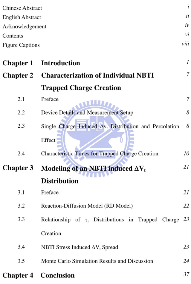
Fig. 1.1 Absolute Static Noise Margin (SNM) change vs. threshold voltage shift (Vt) for different VDD, indicating that the SNM change increases as VDD decreases.
4
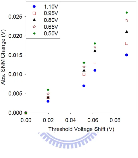
Fig. 1.2 Percentage frequency reduction of NBTI stressed ring oscillator versus supply voltage (VDD). The magnitude of the frequency reduction increases as VDD decreases.
5
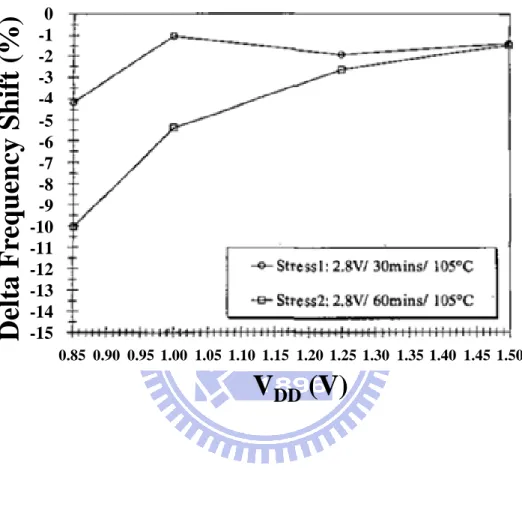
Fig. 1.3 Illustration of an NBTI induced Vt distribution and a device qualification criterion.
6
Chapter 2
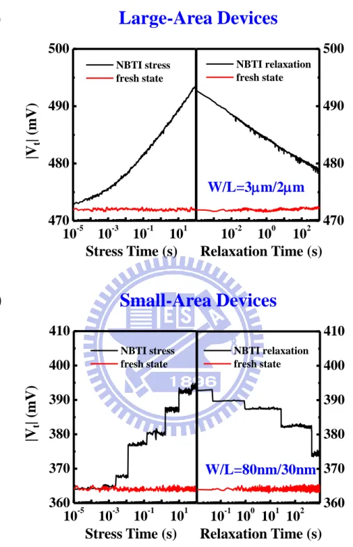
Fig. 2.1 (a) Continuous Vt evolutions in NBTI stress and relaxation in a large-area (W/L=3m/2m) high-k pMOSFET. Vg is −1.8V in stress. T= 25°C.
(b) Stepwise Vt evolutions in NBTI stress and relaxation in a small-area (W/L=80nm/30nm) high-k pMOSFET. Vg is −1.8V in stress. T=25°C. The abrupt Vt shifts represent single-charge trapping and detrapping.
11
Fig. 2.2 We characterize NBTI stress in high-k (HfSiON) gate dielectric and metal gate (TiN) MOSFETs. The devices have a gate length of 30nm, a gate width of 80nm and an equivalent oxide thickness of ~1.0nm.
12
Fig. 2.3 (a) Schematic diagram for NBTI stress transient characterization. (b) The waveforms applied to the gate and the drain in stress and in
ix measurement phases.
Fig. 2.4 log(Id) versus Vg plots before and after 100sec NBTI stress at Vg=−1.8V in a pMOSFET.
14
Fig. 2.5 Example Id and Vt traces in NBTI stress. 1, 2 and 3 are the 1st, the 2nd and the 3rd trapped hole creation times, respectively. vt,i (i = 1, 2, 3) represents a single trapped hole creation induced threshold voltage shift.
15
Fig. 2.6 Illustration of channel surface potential and current pattern. When the trapped charge locates on the main current path, it will induce larger vt amplitude.
16
Fig. 2.7 The magnitude distributions of single-charge induced vt collected from NBTI stress and recovery Vt traces in 130 pMOSFETs. The solid line is drawn as a reference.
17
Fig. 2.8 The probability density distribution of a trapped charge (hole) creation time in NBTI stress. 1, 2, and 3 are the 1st, the 2nd, and the 3rd trapped hole creation times, respectively, in a device. The three log() distributions have a similar shape but are shifted by an amount nlog(i).
18
Fig. 2.9 We calculate the mean (<log(i)>) of the three log(i) distributions and reveal a relationship <log(i)> - <log(1)>~nlog(i). i is a sequence number in trapped charge creation in NBTI stress and n is about 5.6.
19
Table I The mean (<log(i)>) and the standard deviation of the three log(i) distributions. i is a sequence number in trapped charge creation in NBTI stress.
x
Chapter 3
Fig. 3.1 The probability density distributions of log(i)-nlog(i). The solid line represents a Gaussian-distribution fit.
27
Fig. 3.2 NBTI induced Vt versus number of created trapped holes in a device at a stress time of 0.01s (a), 1s (b) and 100s (c). Each data point represents a device. A straight line with a slope of 3.3 mV is drawn as a reference.
28
Fig. 3.3 The mean of the Vt distribution versus NBTI stress time from measurement and from our model.
29
Fig. 3.4 The variance of the Vt distribution versus NBTI stress time from measurement and from our model.
30
Fig. 3.5 A Monte Carlo simulation flowchart. M is the number of precursors in a device. A precursor density of 1×10¹² 1/cm2 is assumed.
31
Fig. 3.6 Probability density distributions of a trapped charge (hole) creation time in a log() scale. The symbols are measurement result and the solid lines are from Monte Carlo simulation.
32
Fig. 3.7 Complementary cumulative distribution functions (1-CDF) of NBTI induced Vt from measurement and from a Monte Carlo simulation. The stress time is 0.01s (a), 1s (b) and 100s (c), respectively. The inset shows the probability distributions of Vt.
33
Fig. 3.8 Comparison of NBTI induced Vt distributions (1-CDF) calculated from this model and from the Poisson distributed trap number model. The dots are measurement result. The stress time is 100 s.
34
xi
from our model and from the Poisson distributed trap number model.
1
Chapter 1
Introduction
The aggressive CMOS scaling has been reaching the physical limit of conventional SiO2 MOSFETs as a result of significant direct tunneling current through ultrathin oxides. High-permittivity (high-k) gate dielectrics have emerged as a post-SiO2 solution. Negative bias temperature instability (NBTI) has been recognized as a major concern in scaled high-permittivity (high-k) gate dielectric p-type metal-oxide-semiconductor field effect transistors (pMOSFETs) because of its significant impact on circuit performance and reliability [1-3]. The use of high-k gate dielectrics even expedites NBTI degradation [4-5]. NBTI caused noise margin degradation in SRAM cell (Fig. 1.1) and frequency degradation in a ring oscillator
(Fig. 1.2) have been reported recently [6-7]. NBTI severity aggravates as supply
voltage reduces in device scaling. In addition to digital circuits, NBTI is of particular importance for analog applications where the ability to match device characteristics to a high precision is critical [8]. For instance, in digital-to-analog converters, NBTI can pose a serious reliability issue as a small Vt shift in bias current source can cause large gain errors [9]. Therefore, it is important to carefully characterize the time evolution of threshold voltage to ensure the long-term viability of an integrated circuit.
As MOSFET reduce to a nanometer scale, the threshold voltage degradation due to NBTI varies considerably from one transistor to another. Two NBTI degradation models, a reaction-diffusion (RD) model [10] and a charge trapping model [11-12], have been proposed. In our earlier work [11], we reported that NBTI induced Vt
2
degradation exhibits two stages. The first stage is ascribed to the charging of pre-existing high-k traps and exhibits a log(t) dependence. The second stage is caused by high-k trap creation and follows power-law dependence on stress time. Since in this work our measured NBTI induced Vt degradation obeys a t1/n dependence (n~5.6), an NBTI Vt distribution model will be developed based on the RD model.
The mean of an NBTI Vt distribution, or a Vt in a large-area device, can be well predicted by the RD model [10, 13-15], but the RD model alone is insufficient to describe an entire Vt distribution in nanoscale transistors. In NBTI qualification, since it is the tail part of a Vt distribution to determine a qualification pass/failure
(Fig. 1.3), an accurate model of an overall Vt distribution and its stress time
evolutions is urgently needed in an NBTI qualification method.
In Chapter 2, we characterize NBTI trap creation and Vt shifts in small-area devices. Unlike a large-area device, NBTI induced Vt degradation proceeds in discrete steps in small-area devices [3, 16]. Due to the discrete nature of a Vt evolution, we are able to measure individual trapped charge creation times and each trapped charge induced Vt shift. A total Vt shift in an NBTI stressed device can be expressed as the sum of each individual trapped charge induced vt, i.e.,
1 ,
N
t i t i
V v
, where N is a total number of stress created traps in a device and vt denotes a single trapped charge caused Vt shift. Two factors influence a Vt distribution. One is the dispersion of vt and the other is fluctuations in number of traps N in stressed devices. Single trapped charge (hole) induced vt and its trapped charge (hole) creation time in NBTI stress are extracted from the measurement data.3
are Gaussian-like distributions. Relationship of i distributions in trapped charge creation are derived by the RD model. A Monte Carlo model employing the RD model, collected the trapped charge creation time distributions and single trapped charge (hole) induced vt distribution will be developed to simulate an NBTI induced
Vt distribution and its stress time evolutions. The mean and variance of Vt are acquired during NBTI stress. In literature, a Poisson distributed trap number was usually assumed [17-19] in an NBTI stressed device to model a Vt distribution. We also compare our model with Poisson model. However, the Poisson model based on a notion that individual trapped charge creations during NBTI stress are independent. In other words, each new trap creation in a device has the same probability regardless of how many traps have been created. Nevertheless, the RD model and measurement result show that NBTI degradation obeys a power-law dependence on stress time, implying that a new trap creation rate decreases with an increasing trapped charge number. Therefore, the use of a Poisson distribution model is contradictory to a measurement result and may exaggerate an NBTI induced Vt distribution tail. Finally, we give a conclusion in Chapter 4.
4
Fig. 1.1 Absolute Static Noise Margin (SNM) change vs. threshold voltage shift (Vt) for different VDD, indicating that the SNM change increases as VDD decreases.
5
Fig. 1.2 Percentage frequency reduction of NBTI stressed ring oscillator versus
supply voltage (VDD). The magnitude of the frequency reduction increases as VDD decreases. 0 -1 -2 -3 -4 -5 -6 -7 -8 -9 -10 -11 -12 -13 -14 -15 0.85 0.90 0.95 1.00 1.05 1.10 1.15 1.20 1.25 1.30 1.35 1.40 1.45 1.50
Delta Fr
equency
Shift
(%
)
V
DD(V)
6
Fig. 1.3 Illustration of an NBTI induced Vt distribution and a device qualification criterion.
Threshold Voltage Shift,
V
tPr
obab
il
ity
Dens
ity
Distribution
Pass/Fail Criterion
7
Chapter 2
Characterization of Individual NBTI
Trapped Charge Creation
2.1 Preface
As device dimensions reduce to a nanometer scale, NBTI induced Vt shifts scatter widely from a device to a device. Modeling of an entire NBTI induced Vt distribution is needed to ensure that the tail of Vt distribution does not cross the reliability criteria in a specified lifetime.
Conventionally, NBTI characterization is carried out by periodically interrupting stress to measure device electrical parameters such as Vt or drain current (Id) degradation. Note that conventional measurement (for example, by Agilent 4156), which usually takes a few seconds between stress and recovery transitions, is unable to catch an initial transient in a s to ms range and may significantly underestimate the magnitude of a transient effect. Owing to recent improvements in measurement techniques [20-22], a measurement delay can be reduced to s (for example, by Agilent B1500) to avoid information missing during a switching transient.
In contrast to large-area devices (Fig. 2.1 (a)), we found that NBTI induced Vt degradation and recovery in nanoscale transistors proceed in discrete steps [22-26]
due to augmentation of single charge effects in scaled devices. Example Vt evolutions in a small-area device (W/L=80nm/30nm) are shown in Fig. 2.1 (b). In the figure, each abrupt Vt change in stress/recovery Vt traces is caused by single charge
8
creation/detrapping in gate dielectrics. Due to the discrete nature of Vt evolutions, we are able to measure individual charge creation/detrapping times and the magnitudes of single charge induced Vt shifts. Statistical characterization of NBTI traps in nanoscale devices helps gain insight into mechanisms in NBTI stress.
2.2 Device Details and Measurement setup
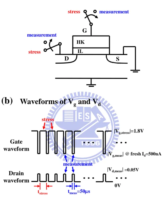
We characterize NBTI stress in high-k (HfSiON) gate dielectric and metal gate (TiN) pMOSFETs. The devices have a gate length of 30nm, a gate width of 80nm and an equivalent oxide thickness (EOT) of ~1.0nm. The device structure we used in this thesis is illustrated in Fig. 2.2.
Schematic diagram for NBTI stress transient measurement is shown in Fig. 2.3 (a). The stress characterization scheme is similar to [27], i.e., in a stress-measurement-stress (SMS) sequence, as shown in Fig. 2.3 (b). In NBTI stress phase, |Vg,stress|=1.8V and Vd=0V at room temperature for 100sec. In measurement phase, the drain voltage |Vd,meas| is 0.05V and the gate voltage |Vg,meas| is chosen such that a pre-stress drain current is ~500nA. Drain current variations (Id) are recorded using Agilent B1500 with a switch delay time less than 1s. A corresponding Vt is obtained from a measured Id divided by a transconductance (gm).
2.3 Single Charge Induced
v
tDistribution and Percolation
Effect
To check on Si surface trap creation in NBTI stress, we monitor transconductance (gm) and subthreshold swing (S) degradations during stress.
9
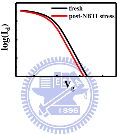
Pre-stress and post-stress subthreshold Id−Vg are shown in Fig. 2.4. An almost parallel shift is noted, suggesting that Vt degradation is mainly caused by trapped charge creation in the bulk of gate dielectrics rather than surface traps. Both S and gm
degradations are less than 5% after the stress. For simplicity, a constant gm is used
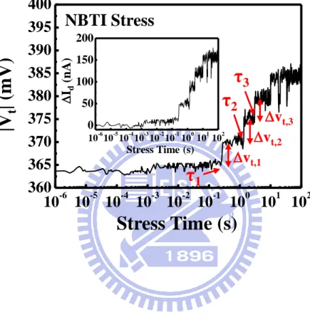
when converting a Id into a Vt. Fig. 2.5 shows example Id and Vt traces in NBTI stress. A small letter (vt,i) denotes a single trapped hole creation induced Vt shift, where i denotes a trapped charge creation sequence number. A capital letter (Vt) is a total Vt shift after stress.
In nanoscale MOSFETs, non-uniform 3D electrostatics and the discreteness and the randomness of substrate dopants determine current percolation paths in a channel
(Fig. 2.6). Thus, each trapped charge creation has specific vt amplitude depending on
its position in a channel.
We measure and record the magnitudes of single-charge induced vt in NBTI stress/recovery Vt traces in ~130 pMOSFETs. The magnitude distributions of the vt are plotted in Fig. 2.7. The measurement resolution is about 1mV. Voltage steps with
vt less than 1mV are not recorded. The collected vt from stress traces and from recovery traces have a similar distribution, characterized by an exponential function
f(|vt|)=exp(−|vt|/amp)/amp with a amp of 3.3mV. A straight line with a slope of
3.3mV is drawn to serve as a reference. The exponential function is an empirical formula. The origin and the dispersion of the vt have been studied thoroughly. In such small-area devices, single-charge induced vt cannot be estimated from its distance to a gate electrode by using a 1D capacitance equation C=/d because of a
10
distribution is realized due to the percolation effect [3, 17-18, 28-29]. A 3D atomistic numerical device simulation shows a similar vt probability function [29].
2.4 Characteristic Times for Trapped Charge Creation
The second factor affecting an NBTI induced Vt distribution is the dispersion of a characteristic time for a trapped hole creation. Individual trapped hole creation times are clearly defined in stress Vt traces, for example, 1, 2 and 3 in Fig. 2.5. We collect the first three trapped hole creation times (i, i=1,2,3) from about 130 devices. The probability density functions (PDFs) of the log(i), i=1,2,3, are shown in Fig. 2.8. It should be remarked that about 3% devices have less than 3 traps created in a stress period of 100sec. The mean (<log(i)>) and the standard deviation of the three log(i) distributions are indicated in Table I. The solid line in Fig. 2.8 is a fit by a Gaussian distribution.
Eq. (2.1)
The trap creation characteristic times scatter over several orders of magnitudes. The wide spread of i is attributed to the dispersion from different local chemistry and 3D electrostatics such as random dopants and edge effects in a nanoscale device. We calculate the mean of each log(i) and reveal a relationship <log(i)>−<log(1)>~nlog(i), as shown in Fig. 2.9.A statistical i distribution model will be developed. 2 2
1
(log( )
)
(log( ))
exp[
]
2
2
f
11
Fig. 2.1 (a) Continuous Vt evolutions in NBTI stress and relaxation in a large-area (W/L=3m/2m) high-k pMOSFET. Vg is −1.8V in stress. T= 25°C. (b) Stepwise Vt evolutions in NBTI stress and relaxation in a small-area (W/L=80nm/30nm) high-k pMOSFET. Vg is −1.8V in stress. T=25°C. The abrupt Vt shifts represent single-charge trapping and detrapping.
10
-510
-310
-110
1470
480
490
500
NBTI stress fresh state10
-210
010
2470
480
490
500
NBTI relaxation fresh state|V
t| (m
V
)
Stress Time (s)
Relaxation Time (s)
W/L=3
m/2
m
Large-Area Devices
10
-510
-310
-110
1360
370
380
390
400
410
NBTI stress fresh state10
-110
010
110
2360
370
380
390
400
410
NBTI relaxation fresh state|V
t| (m
V
)
Stress Time (s)
Relaxation Time (s)
W/L=80nm/30nm
Small-Area Devices
(a)
12
Fig. 2.2 We characterize NBTI stress in high-k (HfSiON) gate dielectric and metal
gate (TiN) MOSFETs. The devices have a gate length of 30nm, a gate width of 80nm and an equivalent oxide thickness of ~1.0nm.
SiON
S
D
HfON
TiN
13
Fig. 2.3 (a) Schematic diagram for NBTI stress transient characterization. (b) The
waveforms applied to the gate and the drain in stress and in measurement phases.
G
D
S
measurement measurement stress stress IL HKSchematic diagram
Waveforms of V
gand V
dGate
waveform
Drain
waveform
|Vg,stress|=1.8V |Vg,meas| |Vd,meas| 0V measurement stress tmeas=50s tstress @ fresh Id=500nA =0.05V(a)
(b)
14
Fig. 2.4 log(Id) versus Vg plots before and after 100sec NBTI stress at Vg=−1.8V in a pMOSFET.
lo
g(
I
d
)
V
g
fresh
post-NBTI stress
15
Fig. 2.5 Example Id and Vt traces in NBTI stress. 1, 2 and 3 are the 1st, the 2nd and the 3rd trapped hole creation times, respectively. vt,i (i = 1, 2, 3) represents a single trapped hole creation induced threshold voltage shift.
10
-610
-510
-410
-310
-210
-110
010
110
2360
365
370
375
380
385
390
395
400
10-610-510-410-310-210-1100101102 0 50 100 150 200 Stress Time (s) Id (nA )τ
2τ
1|V
t|
(mV)
Stress Time (s)
τ
3
v
t,1
v
t,3
v
t,2NBTI Stress
16
Fig. 2.6 Illustration of channel surface potential and current pattern. When the trapped
charge locates on the main current path, it will induce larger vt amplitude.
Drain Current Flux Substrate Dopant
17
Fig. 2.7 The magnitude distributions of single-charge induced vt collected from NBTI stress and recovery Vt traces in 130 pMOSFETs. The solid line is drawn as a reference.
0
5
10
15
20
25
10
-410
-310
-210
-110
0
amp= 3.3 (mV)
Single Charge Induced |
v
t| (mV)
P
ro
ba
bi
li
ty D
ens
it
y
D
is
tri
buti
o
n
| | 1 exp( t ) amp amp v stress
relaxation
18
Fig. 2.8 The probability density distribution of a trapped charge (hole) creation time
in NBTI stress. 1, 2, and 3 are the 1st, the 2nd, and the 3rd trapped hole creation times, respectively, in a device. The three log() distributions have a similar shape but are shifted by an amount nlog(i).
-8 -6 -4 -2 0 2 4 0.00 0.06 0.12 0.18 0.00 0.06 0.12 0.18 0.00 0.06 0.12 0.18
Pr
ob
ab
il
ity
Dens
ity
Distribu
tion
log(
)
132 devices 127 devices 121 devices
1
2
3 1.69 =5.6log(2) 2.67 =5.6log(3)19
Fig. 2.9 We calculate the mean (<log(i)>) of the three log(i) distributions and reveal a relationship <log(i)>-<log(1)>~nlog(i). i is a sequence number in trapped charge creation in NBTI stress and n is about 5.6.
0.0
0.1
0.2
0.3
0.4
0.5
-4.0
-3.5
-3.0
-2.5
-2.0
-1.5
-1.0
-0.5
measured
i<
log(
i)>
log(i)
Slope =5.6
i=1 i=2 i=320
Table I The mean (<log(i)>) and the standard deviation of the three log(i) distributions. i is a sequence number in trapped charge creation in NBTI stress.
trapped hole
creation time
1
2
3mean of log(
)
(<log(
)>)
−3.572 −1.885 −0.906
standard
deviation of log(
)
1.436
1.379
1.282
21
Chapter 3
Modeling of an NBTI induced
V
t
Distribution
3.1 Preface
An NBTI induced Vt distribution in pMOSFETs is explored and characterized. In the previous chapter, we characterize individual trapped charge creation by NBTI stress in a large number of nanoscale high-k pMOSFETs. The time constant (i) distributions of the first three trapped holes (i=1,2,3) are obtained. The mean and the variance of the log(i) are investigated. We find that the characteristic times of a trapped charge creation scatter over several decades of time in nanoscale pMOSFETs, which is attributed to the dispersion from different local chemistry in reaction-diffusion (RD) model and 3D electrostatics such as random dopants and edge effects in a nanoscale device. Two NBTI degradation models, a RD model [10] and a charge trapping model [11-12], have been proposed. Since in this work our measured NBTI induced Vt degradation obeys a t1/n dependence, an NBTI induced Vt distribution model will be developed based on the RD model.
We collect the first three trapped charge creation times (i, i=1,2,3) from about 130 devices. A statistical model for an NBTI induced Vt distribution by employing the RD model and convolving collected the trapped charge creation times (i) and a single trapped charge induced Vt shift is developed. Our model reproduces measurement results of an overall NBTI induced Vt distribution and its stress time evolutions well.
22
3.2 Reaction-Diffusion Model (RD Model)
According to the RD model, the stress time dependence of the number of NBTI generated traps in a device is shown below [10],
Eq. (3.1)
and
Eq. (3.2)
Nt is a total number of NBTI trapped charges in a device (also interpreted as a
sequence number of the last created trapped charge). W is a gate width, L is a gate length, and other variables have their usual definitions in [10]. Three activation energies (EF, ER, Ediffusion) associated with KF, KR, and D in the RD model are lumped
together and activation energy (ED) in Eq. (3.1) is defined as
Eq. (3.3)
By re-arranging the terms in Eq. (3.1), the i-th trapped charge creation time (i) is shown below Eq. (3.4) 1
2
exp(
) exp(
) , ~ 6,
3
D n t BE
F
N
A
t
n
k T
1 6 0 2 3 0 0 [ ][ ] [ F ] . R K SiH h A WLD pK 1 2 ( ). 6 3 D diffusion F R E E E E1
1
2
log( )
log( )
(
) log( ).
2.3
3
D i BE
F
i
A
n
k T
23
3.3 Relationship of
iDistributions in Trapped Charge
Creation
In the following, we re-arranging the terms and taking average in Eq. (3.4) and the relationship of the mean of the log(i) is obtained,
Eq. (3.5)
It should be remarked that a real subtracted amount is 1.69 for log(2) (cf. 6log(2)=1.81) and 2.67 for log(3) (cf. 6log(3) =2.86). The slight difference is in that Eq. (3.5) is derived based on an NBTI evolution rate (t1/n) with n=6 while our measured n is about 5.6 in an initial stress stage. Thus, we obtain <log(2)>−<log(1)>=5.6log(2)=1.69 and <log(3)>−<log(1)>=5.6log(3)=2.67. The calculated result from Eq. (3.5) is in reasonable agreement with the measurement result in Table I.
Furthermore, we can shift the measured log(i) distribution by subtracting a term
nlog(i) from Eq. (3.5). The log(i)−nlog(i) distributions from the 1, 2, and 3,
respectively, are shown in Fig. 3.1. A reasonably good match of the log() distributions from the 1, 2, and 3 is obtained. The solid line in Fig. 3.1 represents a Gaussian-distribution fit. The standard deviation of the Gaussian distribution is about 1.6.
3.4 NBTI Stress Induced
V
tSpread
We measure threshold voltage shifts at different stress times in a number of 1
log( )
ilog( )
n
log( ).
i
24
NBTI stressed pMOSFETs. The number of trapped holes and a total threshold voltage shift (Vt) in each device are recorded. Fig. 3.2 shows the measurement results at a stress time of 0.01s, 1s and 100s, respectively. The y-axis is a total Vt in stress and the x-axis is the number of trapped holes. Each data point represents a device. A straight line with a slope of 3.3mV, i.e., an average single-charge induced Vt shift, is drawn in the figure as a reference. The measurement data scatter along the lines. The
Vt and the number distributions broadenwith stress time.
We extract the mean and the variance of the Vt distributions. An average of Vt in 130 devices is plotted in Fig. 3.3. The mean follows a power law dependence on stress time (t1/n) in five decades of time with n about 6. The variance of the Vt distribution also increases with stress time, as shown in Fig. 3.4. In our earlier work, we reported a two-stage Vt degradation by BTI stress [11]. The first stage is ascribed to the charging of pre-existing high-k dielectric traps and exhibits a log(t) dependence. The second stage degradation is caused by high-k dielectric trap creation and follows a power law dependence on stress time. Note that a log(t) degradation stage is not observed in this work possibly because of no many pre-existing traps in the current samples.
3.5 Monte Carlo Simulation Results and Discussion
A statistical model based on a Monte Carlo (MC) approach is developed. Based on the collected the trapped charge creation times (i) and vt distributions, a Monte Carlo simulation can calculate the number of traps (N) and entire Vt distributions. A Monte Carlo flowchart is shown in Fig. 3.5. In our MC simulation, a trapped charge creation sequence number (i) is assigned to each precursor in a device. The trapped
25
charge creation times (i) of each precursor is chosen according to the Gaussian distribution in Fig. 3.1. A Poisson-distributed precursor number (M) in each device is assumed with a mean value of 24 in an 80nm×30nm device, which corresponds to a precursor density of 1012 cm-2 [30]. Each trapped charge creation time (i) is then shifted according to Eq. (3.5). A trapped charge creation time with the shortest has i
= 1, and the second shortest one has i = 2 and so on. In this approach, we can reproduce the same i distributions (Fig. 3.6).
For a stress time t, the number of trapped charges N is computed by counting all the precursors with i (i=1,2,...,M) less than t. For each counted trapped charge, a single trapped charge induced Vt shift (vt) is randomly selected based on an exponential distribution, f(|vt|)=exp(−|vt|/amp)/amp, with amp=3.3mV. An NBTI
induced Vt at a stress time t can be computed by summing up all the vt, i.e., ,
1
N
t i t i
V v
. In total, 5x10⁵ devices are simulated in Monte Carlo simulation. The mean and the variance of the simulated Vt distributions versus stress time are shownin Fig. 3.3 and Fig. 3.4, respectively. Good agreement between the Monte Carlo
simulation and measurement results is obtained. In addition, we compare measured and simulated Vt distributions at different stress times. Complementary cumulative distribution functions (1-CDF) of NBTI induced Vt at a stress time of t=0.01s, 1s and 100s are plotted in Fig. 3.7. The inset of the figure is the probability density function of Vt. Our simulation is in good agreement with measurement results.
Finally, we also compare this model with the Poisson distributed trap number model [17-19] at a stress time of 100s. To examine the difference in a Vt distribution tail, complementary cumulative distribution functions (1-CDF) of the two models at a
26
stress time of 100s are plotted in Fig. 3.8 with a logarithmic scale in y-axis. The probability density distributions of a trapped charge number from the two models are plotted in Fig. 3.9. The Poisson model apparently yields a broader distribution in trapped charge number (N) and thus a larger NBTI induced Vt tail. The difference between the two models increases with stress time as more trapped charges are created. The reason is that individual trapped charge creations are un-correlated in the Poisson model. In other words, each new trap creation in a device has the same probability regardless of how many traps have been created. Nevertheless, the RD model and measurement results show that NBTI degradation obeys a power-law (t1/n) dependence on stress time, implying that trapped charge creation becomes more difficult as a sequence number of charge creation increases. We also compare NBTI failure rates in 100sec stress from the two models with two Vt failure criteria, Vt > 50mV and 100mV (Table II). The difference between the two models increases as a failure Vt increases. Our model can fit an NBTI distribution tail better.
27
Fig. 3.1 The probability density distributions of log(i)-nlog(i). The solid line represents a Gaussian-distribution fit.
Pr
o
ba
bility
Den
sity
Dis
tributio
n
log(
i) – nlog(i)
-10
-8
-6
-4
-2
0
2
0.00
0.03
0.06
0.09
0.12
0.15
1st trapped hole 2nd trapped hole 3rd trapped hole28
Fig. 3.2 NBTI induced Vt versus number of created trapped holes in a device at a stress time of 0.01s (a), 1s (b) and 100s (c). Each data point represents a device. A straight line with a slope of 3.3 mV is drawn as a reference.
0
20
40
60
80
t = 0.01s
Slope = 3.3mV
0
5
10
15
20
25
0
20
40
60
80
Slope = 3.3mV
t = 100s
0
20
40
60
80
t = 1s
Slope = 3.3mV
Number of Trapped Charges
NBT
I
Indu
ced
|
V
t|
(m
V)
(a)
(b)
(c)
29
Fig. 3.3 The mean of the Vt distribution versus NBTI stress time from measurement and from our model.
10
-210
-110
010
110
21
10
100
Measurement This modelStress Time (s)
|
V
t| (mV)
Slope ~ 1/6
30
Fig. 3.4 The variance of the Vt distribution versus NBTI stress time from measurement and from our model.
10
-210
-110
010
110
20
30
60
90
120
150
180
Measurement This modelV
aria
nce
of
|
V
t|
(mV
2)
Stress Time (s)
31
Fig. 3.5 A Monte Carlo simulation flowchart. M is the number of precursors in a
device. A precursor density of 1×10¹² 1/cm2 is assumed.
, 1 M t t i i V v
i < stress time (t)? Yes i =1 STARTRandom generation of vt,ibased on an exponential distribution
Random generation of ibased on a Gaussian distribution
<log(i)> = <log(1)> + nlog(i)
vt,i= 0 No END Yes No Yes No 5x10⁵ devices simulated? i=i+1, i >M?
32
Fig. 3.6 Probability density distributions of a trapped charge (hole) creation time in a
log() scale. The symbols are measurement result and the solid lines are from Monte Carlo simulation.
-6 -5 -4 -3 -2 -1 0
1
2
0.00
0.06
0.12
0.18
0.24
0.30
1 2 3 1 2 3log (
)
Pr
o
ba
bility
Density
Distribution
Measurement
Monte Carlo
Simulation
33
Fig. 3.7 Complementary cumulative distribution functions (1-CDF) of NBTI induced
Vt from measurement and from a Monte Carlo simulation. The stress time is 0.01s (a), 1s (b) and 100s (c), respectively. The inset shows the probability distributions of
Vt.
0
20
40
60
0.0
0.2
0.4
0.6
0.8
1.0
Measurement MC Simulation0.0
0.2
0.4
0.6
0.8
1.0
Measurement MC Simulation 0 20 40 60 0.0 0.1 0.2 0.3 0.4 0.5 Measurement MC Simulation |Vt| (mV) P r o b ab il ity D is tr ib u ti o n0.0
0.2
0.4
0.6
0.8
1.0
Measurement MC Simulation 0 20 40 60 0.0 0.1 0.2 0.3 0.4 0.5 Measurement MC Simulation |Vt| (mV) P r o b a b il it y Di st r ib u ti o n1
-CDF
t =0.01s
0 20 40 60 0.0 0.1 0.2 0.3 0.4 0.5 Measurement MC Simulation |Vt| (mV) P r o b ab il ity D is tr ib u ti o n|
V
t| (mV)
1
-CDF
1
-CDF
t =1s
t =100s
(a)
(b)
(c)
34
Fig. 3.8 Comparison of NBTI induced Vt distributions (1-CDF) calculated from this model and from the Poisson distributed trap number model. The dots are measurement result. The stress time is 100s.
0
10 20 30 40 50 60 70 80
10
-310
-210
-110
0 Measurement This Model Poisson Model1
-CDF
|
V
t| (mV)
t =100s
35
Fig. 3.9 The probability density distributions of a trapped charge number from our
model and from the Poisson distributed trap number model.
0
4
8
12 16 20
0.0
0.2
0.4
This Model
Poisson Model
Number of Trapped Charges
P
ro
ba
bil
it
y
Densi
ty
Dis
tributio
n
t =100s
36
Table II NBTI failure rates in 100s stress based on two Vt failure criteria.
NBTI Failure
Criterion
Poisson
Model
This Model
Measurement
V
t= 50mV
10.98%
7.62%
9 / 132
37
Chapter 4
Conclusion
A discrete feature in NBTI stress Vt evolutions due to individual trapped charge creations in small-area devices is observed. Single charge creation times and induced Vt shifts are clearly defined. This single charge characterization approach allows us to gain insight into NBTI induced threshold voltage shift distributions in small-area devices. Statistical characterization of individual trapped charge creations in NBTI stress in a large number of nanoscale high-k (HfSiON)/metal gate (TiN) pMOSFETs is performed and an NBTI induced Vt distribution have been investigated.
Two factors are found to influence an NBTI induced Vt distribution. One is the dispersion of single trapped charge induced threshold voltage shift and the other one is the dispersion of trapped charge creation times. The broad distribution of trapped charge creation times is attributed to the dispersion from different local chemistry and 3D electrostatics such as random dopants and edge effects in a nanoscale device.
We develop a statistical model based on measured trap characteristic time distributions to simulate an NBTI induced Vt distribution in nanoscale devices. A correlation between the trapped charge creation distributions and the spread of an NBTI induced Vt distribution has been established. Our model can reproduce a measurement result of an NBTI induced Vt distribution and its stress time evolution well.
38
Reference
[1] S. Pae, J. Maiz, C. Prasad, and B. Woolery, “Effect of BTI Degradation on Transistor Variability in Advanced Semiconductor Technologies,” IEEE Trans.
Device Mater. Rel., vol. 8, no. 3, pp. 519-525, 2008.
[2] S. E. Rauch, “Review and Reexamination of Reliability Effects Related to NBTI-Induced Statistical Variations,” IEEE Trans. Device Mater. Rel., vol. 7, no. 4, pp. 524-530, 2007.
[3] J. P. Chiu, Y. T. Chung, Tahui Wang, Min-Cheng Chen, C. Y. Lu, and K. F. Yu, “A Comparative Study of NBTI and RTN Amplitude Distributions in High-
Gate Dielectric pMOSFETs,” IEEE Electron Device Lett., vol. 33, no. 2, pp. 176-178, 2012.
[4] S. Zafar, Y. H. Kim, V. Narayanan, C. Cabral Jr., V. Paruchuri, B. Doris, J. Stathis, A. Callegari and M. Chudzik, “A Comparative Study of NBTI and PBTI (Charge Trapping) in SiO2/HfO2 Stacks with FUSI, TiN, Re Gates,” in VLSI Symp. Tech.
Dig., pp. 23-25, 2006.
[5] S. Zafar, A. Kumar, E. Gusev and E. Cartier, “Threshold Voltage Instabilities in High-k Gate Dielectric Stacks,” IEEE Trans. Device Mater. Rel., vol. 5, pp. 45-64, 2005.
[6] V. Reddy, A.T. Krishnan, A. Marshall, J. Rodriguez, S. Natarajan, T. Rost, and S. Krishnan, “Impact of Negative Bias Temperature Instability on Digital Circuit Reliability,” in Proc. Int. Relib. Phys. Symp., pp. 248-254, 2002.
[7] A. T. Krishnan, V. Reddy, D. Aldrich, J. Raval, K. Christensen, J. Rosal, C. O’Brien, R. Khamankar, A. Marshall, W-K. Loh, R. McKee, S. Krishnan, “SRAM Cell Static Noise Margin and VMIN Sensitivity to Transistor Degradation,” in IEDM Tech. Dig., pp. 1-4, 2006.
39
[8] M. Agostinelli, S. Lau, S. Pae, P. Marzolf, H. Muthali, and S. Jacobs, “PMOS NBTI-induced circuit mismatch in advanced technologies,” in Microelectron.
Reliab., vol. 46, pp. 63-68, 2006.
[9] N. K. Jha, P. S. Reddy, D. K. Sharma, and V. R. Rao, “NBTI Degradation and Its Impact for Analog Circuit Reliability,” IEEE Trans. Electron Devices, vol. 52, no. 12, pp. 2609-2615, 2005.
[10] A. E. Islam, H. Kufluoglu, D. Varghese, S. Mahapatra, and M. A. Alam, “Recent Issues in Negative-Bias Temperature Instability: Initial Degradation, Field Dependence of Interface Trap Generation, Hole Trapping Effects, and Relaxation,” IEEE Trans. Electron Devices, vol. 54, no. 9, pp. 2143-2154, 2007. [11] C. T. Chan, C. J. Tang, T. Wang, H. C.-H. Wang, and D. D. Tang, “Positive Bias
and Temperature Stress Induced Two-Stage Drain Current Degradation in HfSiON nMOSFET’s,” in IEDM Tech. Dig., pp. 571-574, 2005.
[12] T. Grasser, B. Kaczer, W. Goes, H. Reisinger, T. Aichinger, P. Hehenberger, P.-J. Wagner, F. Schanovsky, J. Franco, M. Toledano, and M. Nelhiebel, “The Paradigm Shift in Understanding the Bias Temperature Instability : From Reaction-Diffusion to Switching Oxide Traps,” IEEE Trans. Electron Devices, vol. 58, no. 11, pp. 3652-3665, 2011.
[13] K. O. Jeppson and C. M. Svensson, “Negative bias stress of MOS devices at high electric fields and degradation of MNOS devices,” J. Appl. Phys., vol. 48, no. 5, pp. 2004-2014, 1977.
[14] S. Ogawa and N. Shiono, “Generalized diffusion-reaction model for the low-field charge build up instability at the Si-SiO2 interface,” Phys. Rev. B, vol. 51, no. 7, pp. 4218-4230, 1995.
40
PMOSFETs,” in IEDM Tech. Dig., pp. 345-348, 2003.
[16] Jung-Piao Chiu, Chi-Wei Li, and Tahui Wang, “Characterization and modeling of trap number and creation time distributions under negative-bias-temperature stress,” Appl. Phys. Lett., vol. 101, no. 8, p. 082906, 2012.
[17] B. Kaczer, T. Grasser, Ph. J. Roussel, J. Franco, R. Degraeve, L.-A. Ragnarsson, E. Simoen, G. Groeseneken, and H. Reisinger, “Origin of NBTI Variability in Deeply Scaled pFRTs,” in Proc. Int. Relib. Phys. Symp., pp. 26-32, 2010.
[18] B. Kaczer, Ph. J. Roussel, and T. Grasser, “Statistics of Multiple Trapped Charges in the Gate Oxide of Deeply Scaled MOSFET Devices—Application to NBTI,” IEEE Electron Device Lett., vol. 31, no. 5, pp. 411-413, 2010.
[19] M. Toledano-Luque, B. Kaczer, J. Franco, P. J. Roussel, T. Grasser, T. Y. Hoffmann, and G. Groeseneken, “From mean values to distributions of BTI lifetime of deeply scaled FETs through atomistic understanding of the degradation,” in VLSI Symp. Tech. Dig., pp. 152-153, 2011.
[20] H. Reisinger, O. Blank, W. Heinrigs, A. Muhlhoff, W. Gustin and C. Schlunder, “Analysis of NBTI Degradation- and Recovery-Behavior Based on Ultra-Fast VT-Measurements”, in Proc. Int. Relib. Phys. Symp., pp. 448-453, 2006.
[21] C. Shen, M. -F. Li, X. P. Wang, Y. -C. Yeo, and D. -L. Kwong, “Fast Measurement Technique of MOSFET Id–Vg Characteristics,” IEEE Electron
Device Lett., vol. 27, no. 1, pp. 55-57, 2006.
[22] T. Wang, C. T. Chan, C. J. Tang, C. W. Tsai, H. C. -H. Wang, M. H. Chi and D. D. Tang, “A Novel Transient Characterization Technique to Investigate Trap Properties in HfSiON Gate Dielectric MOSFETs ─ From Single Electron Emission to PBTI Recovery Transient,” IEEE Trans. Electron Devices, vol. 53, pp. 1073-1079, 2006.
41
[23] C. T. Chan, C. J. Tang, C. H. Kuo, H. C. Ma, C. W. Tsai, H. C. H. Wang, M. H. Chi, and Tahui Wang, “Single-Electron Emission of Traps in HfSiON as High-k Gate Dielectric for MOSFETs”, in Proc. Int. Relib. Phys. Symp., pp. 41-44, 2005. [24] C. T. Chan, H. C. Ma, C. J. Tang and T. Wang, “Investigation of Post-NBTI Stress Recovery in pMOSFETs by Direct Measurement of Single Oxide Charge De-Trapping,” in VLSI Symp. Tech. Dig., pp. 90-91, 2005.
[25] J. P. Chiu, Y. H. Liu, H. D. Hsieh, C. W. Li, M. C. Chen and Tahui Wang, “Statistical Characterization and Modeling of the Temporal Evolutions of Vt Distribution in NBTI Recovery in Nanometer MOSFETs,” IEEE Trans. Electron
Devices, vol. 60, pp. 978-984, 2013.
[26] T. Grasser, H. Reisinger, P.-J. Wagner, W. Goes, F. Schanovsky and B. Kaczer, “The Time Dependent Defect Spectroscopy (TDDS) Technique for the Bias Temperature Instability,” in Proc. Int. Relib. Phys. Symp., pp. 16-25, 2010.
[27] C. T. Chan, C. J. Tang, T. Wang, H. C. -H. Wang, and D. D. Tang, “Characteristics and Physical Mechanisms of Positive Bias and Temperature Stress-Induced Drain Current Degradation in HfSiON nMOSFETs,” IEEE Trans.
Electron Devices, vol. 53, no. 6, pp. 1340-1346, 2006.
[28] A. Asenov, R. Balasubramaniam, A. R. Brown and J. H. Davies, “RTS Amplitudes in Decananometer MOSFETs: 3-D Simulation Study,” IEEE Trans.
Electron Devices, vol. 50, no.3, pp. 839-845, 2003.
[29] S. Amoroso, L. Gerrer, S. Markov, F. Adamu-Lema, and A. Asenov, “Comprehensive statistical comparison of RTN and BTI in deeply scaled MOSFETs by means of 3D ‘atomistic’ simulation,” in Proc. Eur. Solid-State
Device Res. Conf., pp. 109-112, 2012.
42
43