國 立 交 通 大 學
電子工程學系電子研究所
博 士 論 文
低電壓互補式金氧半製程下可相容高工作電壓之
靜電放電防護設計
HIGH-VOLTAGE-TOLERANT ESD PROTECTION
DESIGN IN LOW-VOLTAGE CMOS PROCESSES
研 究 生 :張 瑋 仁 (Wei-Jen Chang)
指導教授 :柯 明 道 (Ming-Dou Ker)
低電壓互補式金氧半製程下可相容高工作電壓之
靜電放電防護設計
HIGH-VOLTAGE-TOLERANT ESD PROTECTION
DESIGN IN LOW-VOLTAGE CMOS PROCESSES
研 究 生:張瑋仁
Student: Wei-Jen Chang
指導教授:柯明道
Advisor: Ming-Dou Ker
國 立 交 通 大 學
電子工程學系電子研究所
博 士 論 文
A Dissertation
Submitted to Department of Electronics Engineering
and Institute of Electronics
College of Electrical and Computer Engineering
National Chiao Tung University
in Partial Fulfillment of the Requirements
for the Degree of Doctor of Philosophy
in
Electronic Engineering
September 2007
Hsinchu, Taiwan, Republic of China
低電壓互補式金氧半製程下可相容高工作電壓
之靜電放電防護設計
研究生:張瑋仁
指導教授:柯明道 博士
國立交通大學電子工程學系電子研究所
摘要
隨著半導體製程的進步與發展,積體電路產品已經成為民生用品般地
大量製造與使用,許多整合多功能的系統晶片(SoC)已經成為各電子公司的
產品研發主力,電子產業也在這個領域有長足的進步與發展。但由於半導
體製造技術的日新月異,使得積體電路對靜電放電防護的能力下降很多,
同時由於操作電壓一直在下降,但是週邊電路的電壓卻未隨半導體製程的
進步而降低,所以在扮演晶片輸入輸出媒介的混合電壓界面(Mixed-Voltage
I/O Interface)上將會產生許多問題,尤其在電子系統訊號整合上。因此要在
此混合電壓電路加上其靜電放電保護電路,需要考量界面電壓轉換、混合
電壓界面間的漏電流
(Leakage Current)、混合電壓界面電路的可靠度
(Reliability)等問題。因此,在混合電壓界面上,如何仔細評估這些問題進
而設計出具有高的靜電放電防護能力的電路將是當今以及未來積體電路設
計上的重要課題,這個主題隨著半導體製程進入 0.13 微米 以及 90 奈米之
後,對積體電路設計產業更加重要。另外,隨著高壓金氧半製程在面版驅
動電路(LCD Driver ICs)、電源供應器(Power Supplies)、電源管理(Power
Management),以及汽車電子(Automotive Electronics)等使用的普及化,對
ii
-於使用在這些應用的輸出端以及當作靜電放電保護元件的高壓電晶體來
說,靜電放電的可靠度問題將比在一般低壓製程的元件來得嚴重,因此如
何有效改善靜電放電耐壓能力,將是這些高壓積體電路設計上很重要的課
題,這個主題也隨著這些產業應用上的多元化而更趨重要。所以本論文分
別針對了混合電壓界面電路以及高壓金氧半製程應用上的限制與困難作討
論,並進一步設計出有效的靜電放電防護電路以適用在各相關應用之積體
電路晶片。
首 先 , 本 論 文 提 出 了 一 種 新 型 的 低 電 壓 驅 動 雙 載 子 接 面 電 晶 體
(Low-Voltage-Triggered PNP, LVTPNP) 來 當 作 混 合 電 壓 輸 入 輸 出 界 面
(Mixed-Voltage I/O Interfaces)之靜電放電保護元件。此新型靜電放電保
護元件是在
CMOS 製程中寄生的雙載子接面電晶體的 N 型井(N-Well)以
及
P 型基板(P-Substrate)接面上,額外植入 N 型或是 P 型的擴散離子所
構成,以降低
N 型井以及 P 型基板接面的崩潰電壓,當輸入電壓比 VDD
高(Over-VDD)或比 VSS 低(Under-VSS)時,不會有漏電以及閘極氧化
層的可靠度問題。在
0.35 微米互補式金氧半製程,已經驗證了此低電壓驅
動雙載子接面電晶體會比傳統寄生的雙載子接面電晶體的靜電放電耐受程
度來得高,而該元件的最佳化佈局方式(Layout Style)也在 0.35 微米以及
0.25 微米互補式金氧半製程中驗證來提升元件本身的靜電放電耐受程度,
經由實驗證明,具有多指狀(Multi-Finger)佈局方式的元件靜電放電耐受
程度會比單指狀(Single Finger)的要來得高。除此之外,在 0.25 微米製程
的晶片驗證下,具有多指狀佈局方式的低電壓驅動雙載子接面電晶體搭配
電源間的靜電放電箝制電路(Power-Rail ESD Clamp Circuit)成功地提升了
非同步數位用戶專線(Asymmetric Digital Subscriber Line, ADSL)輸入級的
靜電放電耐受程度,此輸入級的訊號界於
5V 到-1V 之間,此電壓同時超過
了該
IC 之 VDD(2.5V)和低過了該 IC 之 VSS(0V)。
本論文研究的第二部分,為了提供有效的靜電放電防護於
1.2/2.5V 混
合電壓輸入輸出界面,本論文提出了新型的靜電放電保護架構並在
0.13 微
米製程中成功驗證,此架構同時利用了靜電放電匯流排(ESD BUS)以及
可耐高工作電壓之靜電放電箝制電路(High-Voltage-Tolerant ESD Clamp
Circuit)來實現。當混合電壓輸入輸出界面的銲墊(Pad)對 VDD(或 VSS)
之間遭受靜電轟擊或是輸入輸出腳對腳(Pin-to-Pin)之間遭受靜電轟擊時,
此靜電放電保護架構都可以提供相對應的放電路徑來避免內部電路遭受靜
電損壞。在此靜電放電防護電路中,可耐高工作電壓之靜電放電箝制電路
都是利用
1.2V 低壓元件來實現,並可安全地在 2.5V 的電壓偏壓下工作而
不會有閘極氧化層的可靠度問題。由實驗可知,比起一般的堆疊式電晶體
(Stacked-NMOS)而言,基板觸發(Substrate Triggered)技術可以有效提
升該可耐高工作電壓之靜電放電箝制電路的導通速度以及靜電放電耐受程
度。在堆疊式電晶體的元件尺寸為
480μm/0.2μm 的大小之下,1.2/2.5V 的
混合電壓輸入輸出界面之人體放電模式靜電放電耐壓能力(HBM ESD
levels)可以從原本的 5kV 增加到 6.5kV;同時,機械放電模式靜電放電耐壓
能力(MM ESD levels)可以從原本的 275V 增加到 400V。
本 論 文 研 究 的 第 三 部 份 , 為 了 提 升 應 用 在 車 用 電 子 (
Automotive
Electronics)中的真空螢光顯示器(Vacuum-Fluorescent-Display, VFD)驅
動
IC 的靜電放電耐受程度,本論文提出一種新型的靜電放電保護的元件結
構。此元件結構是在高壓
P 型的金氧半電晶體(HVPMOS)的汲極當中植
入一個
N 型離子佈植來形成一個嵌入式高壓 P 型矽控整流器(High-Voltage
P-Type Silicon Controlled Rectifier, HVPSCR)路徑,此結構只需要加入額外
的
N 型離子局部佈局面積即可實現。在 0.5 微米的互補式金氧半製程中,
成功驗證了具有此嵌入式高壓
P 型矽控整流器的真空螢光顯示器驅動積體
電路的人體放電模式靜電放電耐壓能力可以從不到
500V 增加到 8kV;同
iv
-時,當元件尺寸為
500μm/2μm、600μm/2μm 以及 800μm/2μm 時,機械放
電模式之靜電放電耐壓能力可以通過
1100V、1300V 以及 1900V 的靜電測
試。此外,此嵌入式高壓
P 型矽控整流器的真空螢光顯示器驅動積體電路
可成功通過
±200mA 的閂鎖(Latchup)測試。
本論文研究的第四部分,觀察到使用在輸出端以及當作靜電放電保護
元件的高壓電晶體,靜電放電的可靠度問題比在一般製程的元件來得嚴
重,因此本論文利用
40-V 金氧半製程對於不同元件結構以及汲極到閘極的
距離(Layout Spacing from Drain to Polygate)做一深入探討。實驗結果成
功驗證了汲極下端沒有植入的飄移摻雜(Drift Implant)佈局的高壓金氧半
電晶體比起汲極下端有加入移摻雜的高壓金氧半電晶體有較高的二次崩潰
電流(Secondary Breakdown Current, It2)以及較好的靜電放電防護能力。
在所有元件結構當中,嵌入在高壓
N 型的金氧半電晶體中的高壓 N 型矽控
整流器(HVNSCR)並在汲極下端移除了飄移摻雜的結構,具有最高的二
次崩潰電流以及靜電放電耐受度。此外,元件模擬技巧也成功地分析了有
無飄移摻雜對於元件內電流分佈的影響。
本論文分別針對了混合電壓界面電路以及高壓金氧半製程應用上的限
制與困難作討論,並進一步設計出有效的靜電放電防護電路應用在各相關
之積體電路晶片。本博士論文所提出電路已經有相對應的國際期刊與會議
論文發表以及專利申請。
HIGH-VOLTAGE-TOLERANT ESD PROTECTION DESIGN
IN LOW-VOLTAGE CMOS PROCESSES
Student: Wei-Jen Chang Advisor: Dr. Ming-Dou Ker
Department of Electronics Engineering and Institute of Electronics
National Chiao Tung University
ABSTRACT
The scaling trend of the CMOS technology is toward the nanometer region to increase the speed and density of the transistors in integrated circuits. Due to the reliability issue, the power supply voltage is also decreased with the advanced technologies. However, in an electronic system, some circuits could be still operated at high voltage levels. If the circuits realized with low-voltage devices are operated at high voltage levels, the gate-oxide breakdown and leakage issues will occur. Therefore, for the CMOS integrated circuits (ICs) with the mixed-voltage I/O interfaces, the on-chip electrostatic discharge (ESD) protection circuits will meet more design constraints and difficulties. The on-chip ESD protection circuit for mixed-voltage I/O interfaces should meet the gate-oxide reliability constraints and prevent the undesired leakage current paths during normal circuit operating operation. During ESD stress condition, the on-chip ESD protection circuit should provide effective ESD protection for the internal circuits. In high-voltage CMOS technology, high-voltage transistors have been widely used for display driver ICs, power supplies, power management, and automotive electronics. The high-voltage MOSFET was often used as the ESD protection device in the high-voltage CMOS ICs, because it can work as both of output driver and ESD protection device simultaneously. With an ultra-high operating voltage, the ESD robustness of high-voltage MOSFET is quite weaker than that of low-voltage MOSFET. Hence, how to improve the ESD robustness of HV NMOS with a reasonable silicon area is indeed an
important reliability issue in HV CMOS technology. In this thesis, some new ESD protection structures are proposed to improve ESD robustness of the high-voltage IC products fabricated in CMOS technology.
To protect the mixed-voltage I/O interfaces for signals with voltage levels higher than VDD (over-VDD) and lower than VSS (under-VSS), ESD protection design with the low-voltage-triggered PNP (LVTPNP) device in CMOS technology is proposed. The LVTPNP is realized by inserting N+ or P+ diffusion across the junction between N-well and P-substrate of the PNP device. The LVTPNP devices with different structures have been investigated and compared in CMOS processes. The experimental results in a 0.35-μm CMOS process have proven that the ESD level of the proposed LVTPNP is higher than that of the traditional PNP device. Furthermore, layout on LVTPNP device for ESD protection in mixed-voltage I/O interfaces is also optimized in this work. The experimental results verified in both 0.35-μm and 0.25-μm CMOS processes have proven that the ESD levels of the LVTPNP drawn in the multi-finger layout style are higher than that drawn in the single finger layout style. Moreover, one of the LVTPNP devices drawn with the multi-finger layout style has been used to successfully protect the input stage of an ADSL IC in a 0.25-μm salicided CMOS process.
To increase the system-on-chip ESD immunity of micro-electronic products against system-level ESD stress, the chip-level ESD/EMC protection design should be enhanced. Considering gate-oxide reliability, a new ESD protection scheme with ESD_BUS and high-voltage-tolerant ESD clamp circuit for 1.2/2.5 V mixed-voltage I/O interfaces is proposed in this chapter. The devices used in the high-voltage-tolerant ESD clamp circuit are all 1.2 V low-voltage NMOS/PMOS devices which can be safely operated under the 2.5 V bias conditions without suffering from the gate-oxide reliability issue. The four-mode (PS, NS, PD, and ND) ESD stresses on the mixed-voltage I/O pad and pin-to-pin ESD stresses can be effectively discharged by the proposed ESD protection scheme. The experimental results verified in a 0.13 μm CMOS process have confirmed that the proposed new ESD protection scheme has high human-body-model (HBM) and machine-model (MM) ESD robustness with a fast turn-on speed. The proposed new ESD protection scheme, which is designed with only low-voltage devices, is an excellent and cost-efficient solution to protect mixed-voltage I/O interfaces.
To greatly improve ESD robustness of the vacuum-fluorescent-display (VFD) driver IC for automotive electronics applications, a new electrostatic discharge protection structure of
high-voltage P-type silicon controlled rectifier (HVPSCR) embedded into the high-voltage PMOS device is proposed. By only adding the additional N+ diffusion into the drain region of high-voltage PMOS, the TLP-measured secondary breakdown current (It2) of output driver has been greatly improved greater than 6A in a 0.5-µm high-voltage CMOS process. Such ESD-enhanced VFD driver IC, which can sustain HBM ESD stress of up to 8kV, has been in mass production for automotive applications in car without latchup problem. Moreover, with device widths of 500μm, 600μm, and 800μm, the MM ESD levels of the HVPSCR are as high as 1100V, 1300V, and 1900V, respectively.
The dependences of drift implant and layout parameters on ESD robustness in a 40-V CMOS process have been investigated in silicon chips. From the experimental results, the HV MOSFETs without drift implant in the drain region have better TLP-measured It2 and ESD robustness than those with drift implant in the drain region. Furthermore, the It2 and ESD level of HV MOSFETs can be increased as the layout spacing from the drain diffusion to polygate is increased. It was also demonstrated that a specific test structure of HV n-type silicon controlled rectifier (HVNSCR) embedded into HV NMOS without N-drift implant in the drain region has the excellent TLP-measured It2 and ESD robustness. Moreover, due to the different current distributions in HV NMOS and HVNSCR, the dependences of the TLP-measured It2 and HBM ESD levels on the spacing from the drain diffusion to polygate are different.
In this thesis, the novel ESD protection circuits have been developed for mixed-voltage I/O interfaces and high-voltage CMOS process with high ESD robustness. Each of the ESD protection circuits has been successfully verified in the testchips.
ACKNOWLEDGEMENTS
在交通大學電子研究所的生涯中,首先要感謝我的指導教授柯明道教授
在碩士班和博士班這幾年當中提供我最好的研究環境和資源,並耐心的指導
與鼓勵,使我能順利完成博士學業。在指導教授循序漸進的教誨下,讓我得
以在積體電路靜電放電設計領域中,由入門到能夠解決問題,同時,也不厭
其煩地教導我做研究的方法與論文寫作的技巧。此外,不只在專業領域上的
知識,從柯教授認真的研究態度和嚴謹的處事原則,也讓我學習到克服困難、
解決問題的正確態度與方法,以及如何團隊合作把一件事情有效率地處理
好。雖然過程艱辛,也經歷不少挫折,卻讓我獲益良多,也讓我這幾年成長
許多。
此外,很感謝
307 實驗室另外四位師長,吳重雨校長、吳錦川教授、吳
介琮教授以及陳巍仁教授給我的指導與建議。其中,在我遭遇瓶頸的時候,
由於吳校長在公開場合給學生一席話的啟發,讓我瞭解一個新的 idea,是需
要長時間的努力累積之下,在突發奇想中產生的。還有感謝周世傑教授、方
偉騏教授、謝詠芬博士、姜信欽博士在百忙之中抽空來擔任我的口試委員,
給我指導跟建議,讓整個論文更加完整。
再來非常感謝財團法人聯發科技教育基金會提供優渥的獎學金,在這麼
多優秀的申請者當中獲得這項殊榮,真的感到萬分榮幸,讓我可以無後顧之
憂的情形下專心從事研究,同時也減輕了家中的經濟負擔。
感謝
307 實驗室的羅文裕學長以及徐國鈞博士,在我初來到柯教授研究
群時,給我許多研究和學業上的建議與幫助。感謝碩士班期間,一起在
527
奮鬥的成員郭秉捷、莊凱嵐、黃如琳、陳正瑞、李權哲、周政賢、林棋樺,
有了你們再苦的日子也笑得出來。還有謝謝其他
307 實驗室的成員林昆賢博
士、陳世倫博士、許勝福博士、陳榮昇博士、施育全博士、李瑞梅博士,王
文傑、徐新智、顏承正、蕭淵文、李健銘、陳世宏、陳志豪、陳穩義、吳偉
琳、陳煒明、賴泰翔、王暢資、王資閔、林群佑、陳世範、黃曄仁等學長姐、
同學、學弟們在課業、研究、生活上的幫忙與協助,讓我順利完成我的博士
論文、並學習到做人處事上的態度與方法。此外,感謝
307 實驗室的助理卓
慧貞小姐在實驗室行政事務上的許多協助。
致上最深的感謝給我親愛的家人們,祖父張孟源先生、父親張智鐸先生、
母親莊月梅女士、大妹張育菁、小妹張育慈以及其他家人們。有了您們的支
持、鼓勵、陪伴和照顧,才能讓我順利完成學業。最後謝謝所有幫助我、陪
著我成長的人。謝謝你們。
張 瑋 仁
謹誌於竹塹交大
96 年 秋
CONTENTS
ABSTRACT (CHINESE)
iABSTRACT
(ENGLISH)
v
ACKNOWLEDGEMENTS
viiiCONTENTS
ixTABLE CAPTIONS
xiiiFIGURE CAPTIONS
x i vCHAPTER 1 INTRODUCTION
1
1.1 Background 1
1.2 Issue of Mixed-Voltage I/O Interfaces 1
1.3 Issue of High-Voltage CMOS ICs 4
1.4 Thesis Organization 5
Figures 7
CHAPTER 2 OVERVIEW ON ESD PROTECTION DESIGN FOR
MIXED-VOLTAGE I/O CIRCUITS
112.1 Substrate-Triggered Stacked-NMOS Device 11
2.2 Extra ESD Device between I/O Pad and VSS 13
2.3 Extra ESD Device between I/O Pad and VDD 15
2.4 ESD Protection Design with ESD Bus 16
2.5 Special Applications 17
2.6 Summary 18
Figures 19
CHAPTER 3 ESD PROTECTION DESIGN WITH
LOW-VOLTAGE-TRIGGERED PNP (LVTPNP)
x
-25 3.1 ESD Protection Design with LVTPNP Device 25
3.1.1 Device Structures and TLP-Measured I-V Characteristics 26 3.1.2 Layout Parameters of LVTPNP Devices on HBM ESD Levels 27 3.1.3 Multi-Finger Layout Style for LVTPNP 29
3.2 Application in ADSL Interface 31
3.2.1 ESD Protection Design with LVTPNP for Input Stage of ADSL 31 3.2.2 HBM ESD Levels of ADSL with the Type3 LVTPNP 33
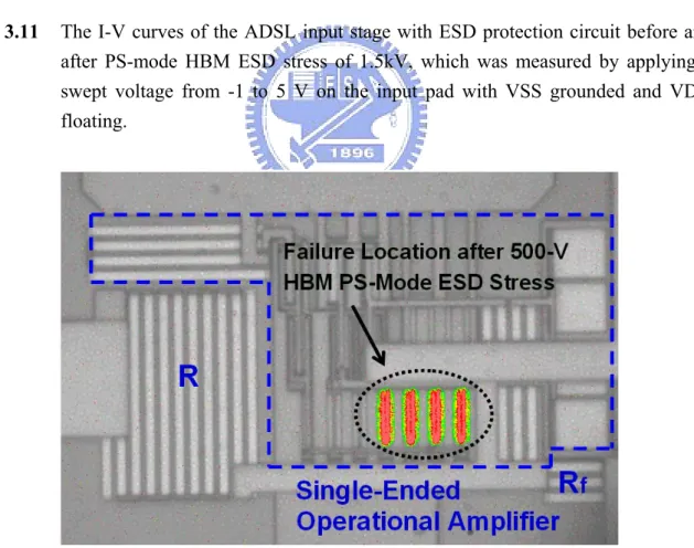
3.2.3 Failure Analysis 34
3.3 Summary 34
Tables 36
Figures 40
CHAPTER 4 HIGH-VOLTAGE-TOLERANT ESD CLAMP
CIRCUIT IN LOW-VOLTAGE THIN-OXIDE
TECHNOLOGY
554.1 ESD Protection Scheme for Mixed-Voltage I/O Interface 55
4.2 High-Voltage-Tolerant ESD Clamp Circuit 57
4.2.1 Substrate-Triggered STNMOS 57
4.2.2 Operation Principle 58
4.2.3 H-Spice Simulated Results 59
4.3 Experiment Results 60
4.3.1 Characteristics of Substrate-Triggered STNMOS 60 4.3.2 Turn-on Speed 61
4.3.3 ESD Robustness of STNMOS Devices 62
4.4 Summary 62
Tables 63
CHAPTER 5 ESD PROTECTION DESIGN FOR AUTOMOTIVE
VACUUM-FLUORESCENT-DISPLAY (VFD)
DRIVER IC
725.1 Original Design for VFD I/O 72
5.1.1 Device Structure and I-V Characteristic of the HVPMOS 73
5.1.2 ESD robustness and Failure Analysis 73
5.2 New ESD Design for VFD I/O 74
5.2.1 Device Structure and Turn-on Mechanism of the HVPSCR 74 5.2.2 ESD Protection Design for VFD I/O with Both HVPSCR and
Power-Rail ESD Clamp Circuit 76
5.3 Experimental Results 77
5.3.1 I-V Characteristic of the HVPSCR 77
5.3.2 ESD robustness of the VFD Driver IC 79
5.4 Summary 79
Tables 81
Figures 82
CHAPTER 6 ESD ROBUSTNESS OF ON-CHIP ESD
PROTECTION DEVICES IN 40-V CMOS
TECHNOLOGY
966.1 Device Structures in 40-V CMOS Process 96
6.1.1 HV NMOS With or Without N-Drift Implant 97 6.1.2 HV PMOS With or Without P-Drift Implant 97 6.1.3 HVNSCR With or Without N-Drift Implant 98
6.2 Experimental Results and Discussion 99
6.2.1 TLP-Measured I-V Characteristics 99
6.2.2 HBM ESD Robustness 103
6.2.3 Failure Analysis 105
6.3 Summary 105
xii
-Figures 107
CHAPTER 7 CONCLUSIONS AND FUTURE WORK
1207.1 Main Results of This Thesis 120
7.2 Future Works 122
REFERNCES
123VITA
131TABLE CAPTIONS
CHAPTER 3
Table 3.1 Breakdown voltage and breakdown current of the LVTPNP devices under both
positive-to-VSS and negative-to-VSS ESD-stress conditions. 36
Table 3.2 HBM ESD Levels of the LVTPNP devices with different layout styles under
positive-to-VSS ESD-stress condition. 37
Table 3.3 HBM ESD Levels of the LVTPNP devices with different layout styles under
negative-to-VSS ESD-stress condition. 38
Table 3.4 HBM ESD Levels of ADSL input stage with different ESD protection designs
under PS-mode, NS-mode, PD-mode, and ND-mode ESD-stress conditions. 39
CHAPTER 4
Table 4.1 HBM and MM ESD levels of STNMOS with or without ESD detection circuit.
63
CHAPTER 5
Table 5.1 TLP_It2 and HBM ESD levels under negative-to-VDD ESD stresses of the
HVPMOS. 81
Table 5.2 TLP_It2, HBM and MM ESD levels under negative-to-VDD ESD stresses of the
HVPSCR. 81
CHAPTER 6
Table 6.1 TLP-measured It2 of HV GGNMOS and HV GDPMOS with or without drift
implant under different spacings D. 106
Table 6.2 TLP-measured It2 of HV GGNMOS and HVNSCR with or without drift implant
FIGURE CAPTIONS
CHAPTER 1
Fig. 1.1 The four pin-combination modes for ESD test on an IC product: (a) positive-to-VSS (PS-mode), (b) negative-to-VSS (NS-mode), (c) positive-to-VDD (PD-mode), and (d) negative-to-VDD (ND-mode). 7
Fig. 1.2 Typical on-chip ESD protection circuits in a CMOS IC. 7
Fig. 1.3 Typical circuit diagrams for (a) the traditional CMOS I/O buffer, and (b) the mixed-voltage I/O circuits with the stacked-NMOS and the N-well self-biased
PMOS. 8
Fig. 1.4 The ESD current paths of (a) the traditional I/O pad with power-rail ESD clamp circuit, and (b) the mixed-voltage I/O pad with power-rail ESD clamp circuit, under the positive-to-VSS (PS-mode) ESD stress. The ESD current paths are
indicated by the dashed lines. 9
Fig. 1.5 The I-V curves in high-current region of single NMOS and stacked-NMOS. 10
Fig. 1.6 The input signals with voltage levels higher than VDD and lower than VSS in some mixed-voltage I/O interfaces. 10
CHAPTER 2
Fig. 2.1 (a) Finger-type layout pattern, and (b) the corresponding cross-sectional view, of the substrate-triggered stacked-NMOS device for mixed-voltage I/O circuits. 19
Fig. 2.2 Schematic circuit diagram of the substrate-triggered stacked-NMOS device with substrate-triggered circuit I for the mixed-voltage I/O circuits. 20
Fig. 2.3 Schematic circuit diagram of the substrate-triggered stacked-NMOS device with substrate-triggered circuit II for the mixed-voltage I/O circuits. 20
Fig. 2.4 (a) ESD protection design with substrate-triggered lateral n-p-n BJT device to protect the mixed-voltage I/O circuits. (b) Cross-sectional view of the lateral n-p-n BJT device in a thin-epi CMOS process. 21
Fig. 2.5 (a) ESD protection circuit with the SNTSCR device to protect the mixed-voltage I/O circuits. (b) Realizations of the SNTSCR device and the ESD detection circuit with the gate-coupling technique to trigger on the SNTSCR device. 22
Fig. 2.6 ESD protection design with the diode string connected between the I/O pad and VDD power line to protect the mixed-voltage I/O circuits. 23
Fig. 2.7 ESD protection design with gated p-n-p BJT as the ESD clamp device connected between I/O pad and VDD to protect the mixed-voltage I/O circuits. 23
Fig. 2.8 The ESD protection network with the additional ESD bus line for the mixed-voltage I/O circuits. One power-rail ESD clamp circuit is connected between VDD power line and VSS power line. A second power-rail ESD clamp
circuit is connected between ESD bus line and VSS power line. 24
Fig. 2.9 High-voltage-tolerant ESD protection design with the forward-biased diode in series with one stacked nMOS for analog ESD protection to reduce the input
parasitic capacitance. 24
CHAPTER 3
Fig. 3.1 The new proposed ESD protection design with LVTPNP device for the mixed-voltage I/O interface with input voltage levels higher than VDD and lower
than VSS. 40
Fig. 3.2 The device structures of (a) the traditional PNP, (b) the type1 LVTPNP, (c) the type2 LVTPNP, (d) the type3 LVTPNP, (e) the gated1 LVTPNP, and (f) the
gated2 LVTPNP. 41
Fig. 3.3 The TLP-measured I-V curves among traditional PNP and different LVTPNP devices under (a) the positive-to-VSS (PS-mode), and (b) the negative-to-VSS
(NS-mode), stress conditions. 42
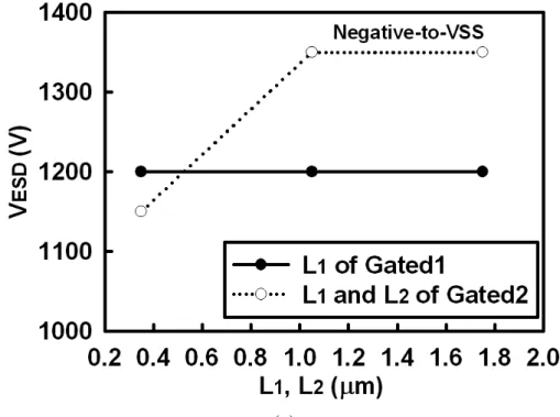
Fig. 3.4 (a) The ESD level v.s. device width under the positive-to-VSS ESD-stress condition. (b) The ESD level v.s. device width under the negative-to-VSS ESD-stress condition. (c) The ESD level v.s. the spacing X of the type1 LVTPNP or the spacing Y of the type2 LVTPNP under the positive-to-VSS ESD-stress condition. (d) The ESD level v.s. the spacing S under the negative-to-VSS ESD-stress condition, respectively. (e) The ESD level v.s. device LE under the negative-to-VSS ESD-stress condition. (f) The ESD level v.s. L1 or L2 of the gated1 LVTPNP and the gated2 LVTPNP under the positive-to-VSS ESD-stress condition. (g) The ESD level v.s. L1 or L2 the gated1 LVTPNP and the gated2 LVTPNP under the negative-to-VSS ESD-stress condition. 43
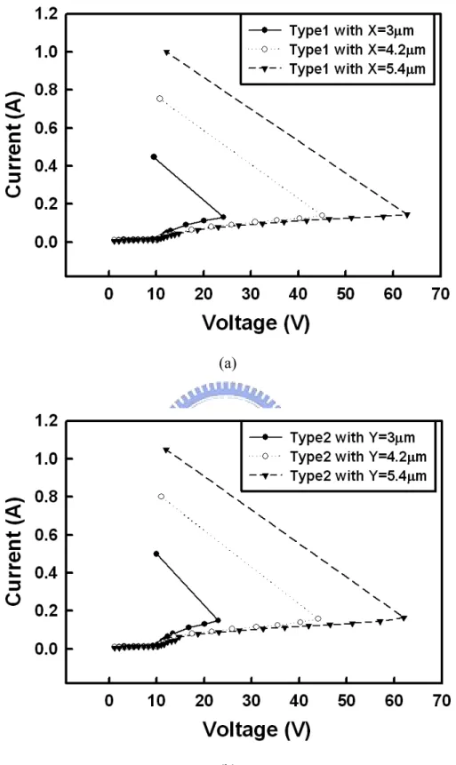
Fig. 3.5 The TLP-measured I-V curves of (a) the type1 LVTPNP with different X spacings, and (b) the type2 LVTPNP with different Y spacings, under the
positive-to-VSS stress condition. 47
Fig. 3.6 (a) The single finger layout style of the LVTPNP, and (b) the cross-sectional view along the line AA’ in the single finger layout of LVTPNP. 48
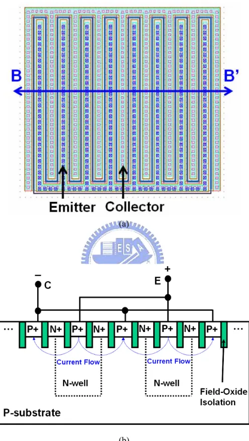
Fig. 3.7 (a) The multi-finger layout style of the LVTPNP, and (b) the cross-sectional view along the line BB’ in the multi-finger layout of LVTPNP. 49
Fig. 3.8 The TLP-measured I-V curves of the LVTPNP devices realized with the single finger layout style or the multi-finger layout style in a 0.25-μm salicided CMOS process under (a) the positive-to-VSS, and (b) the negative-to-VSS, stress
conditions. 50
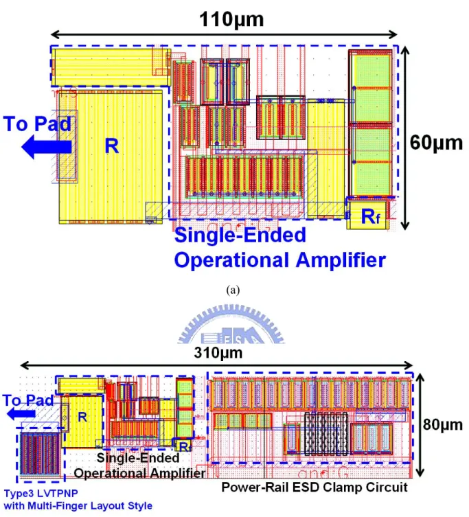
Fig. 3.9 (a) ESD protection design for the ADSL input stage with single-ended operational amplifier and voltage divider in a 0.25-µm salicided CMOS process.
(b) The schematic of the two-stage operational amplifier. 51
Fig. 3.10 The layout views of the ADSL input stage (a) without ESD protection, and (b)
with ESD protection circuit. 52
Fig. 3.11 The I-V curves of the ADSL input stage with ESD protection circuit before and
after PS-mode HBM ESD stress of 1.5kV, which was measured by applying a swept voltage from -1 to 5 V on the input pad with VSS grounded and VDD
floating. 53
Fig. 3.12 The EMMI picture on the ADSL input stage without ESD protection circuit after
HBM PS-mode ESD stress of 500V. 53
Fig. 3.13 The OBIRCH picture on the ADSL input stage with ESD protection circuit after
1.5-kV HBM PS-mode ESD stress. The failure location is on the type3 LVTPNP device of ESD protection circuit. 54
CHAPTER 4
Fig. 4.1 The proposed new ESD protection scheme for 1.2 V/2.5 V mixed-voltage I/O interfaces with a high-voltage-tolerant ESD clamp circuit. 64
Fig. 4.2 The shared ESD_BUS and high-voltage-tolerant ESD clamp circuit for the whole set of I/O cells to achieve pin-to-pin ESD protection. 64
Fig. 4.3 The proposed high-voltage-tolerant ESD clamp circuit. 65
Fig. 4.4 (a) The finger-type layout pattern and (b) the corresponding cross-sectional view of the substrate-triggered STNMOS device. 66
Fig. 4.5 The operation of the high-voltage-tolerant ESD clamp circuit during normal
circuit operating conditions. 67
Fig. 4.6 The operation of the high-voltage-tolerant ESD clamp circuit during a PS-mode
ESD stress event. 67
Fig. 4.7 The Hspice-simulated voltage waveforms of the ESD detection circuit during
normal power-on transition. 68
Fig. 4.8 The Hspice-simulated voltage waveforms of the ESD detection circuit during
ESD stress event. 68
Fig. 4.9 (a) The measured DC I-V curves of the STNMOS device under different substrate-triggered currents. (b) The measured βF-IC relation of the STNMOS
device. 69
Fig. 4.10 The TLP-measured I-V curves of the STNMOS device with the device dimension
(W/L) of 360 μm/0.2 μm under different substrate-triggered currents. 70
Fig. 4.11 The TLP-measured I-V curve of the STNMOS with or without ESD detection
circuit under device dimension (W/L) of 360 μm/0.2 μm. 70
Fig. 4.12 The TLP-measured It2 of the STNMOS device with or without the ESD detection
Fig. 4.13 The measured voltage waveform of STNMOS with or without the ESD detection
circuit under 0 to 20V voltage pulse with a rise time of 10 ns on the ESD_BUS
pad. 71
CHAPTER 5
Fig. 5.1 The original output cell of the automotive VFD driver IC realized with the high-voltage PMOS (HVPMOS) and pull-down resistor. 82
Fig. 5.2 The device structure of HVPMOS in the specific CMOS process. A HV P-well is used to surround the drain of HVPMOS to meet the HV application. 83
Fig. 5.3 The DC I-V curve of HVPMOS in low-current region, which has a breakdown
voltage of 65V. 83
Fig. 5.4 The TLP-measured I-V curves of HVPMOS (a) with a width of 600µm and a length of 2µm, and (b) with a width of 800µm and a length of 2µm. 84
Fig. 5.5 The measured I-V curves of the HVPMOS (with a width of 600µm and a length of 2µm) in VFD driver I/O cell before and after 1-kV ND-mode HBM ESD stress.
85
Fig. 5.6 The SEM failure pictures of (a) the output HVPMOS with device width of 600μm and length of 2µm, (b) the contact spiking in the source region of HVPMOS, and (c) the contact spiking in the drain region of HVPMOS, in the VFD driver IC after 1-kV negative-to-VDD HBM ESD stress. 86
Fig. 5.7 The new proposed ESD protection design with the high-voltage p-type SCR (HVPSCR) embedded into the output HVPMOS to improve ESD robustness of output cell of the automotive VFD driver IC. 88
Fig. 5.8 The device structure of the HVPSCR embedded into the output HVPMOS. 89
Fig. 5.9 The equivalent circuit of the HVPMOS with the embedded HVPSCR. 89
Fig. 5.10 The circuit schematic of the power-rail ESD clamp circuit which is composed by
resistor, capacitor, inverter and NMOS. 90
Fig. 5.11 The ESD current paths on the VFD driver IC with HVPSCR and power-rail ESD
clamp circuit under (a) positive-to-VSS (PS-mode), (b) negative-to-VSS (NS-mode), (c) positive-to-VDD (PD-mode), and (d) negative-to-VDD
(ND-mode) ESD-stress conditions. 91
Fig. 5.12 The DC I-V curves of the HVPSCR (a) with a DC trigger voltage of 65V and a
holding voltage (current) of ~ 5V (~ 35mA) under the temperature of 25°C, and (b) with a DC trigger voltage of 65V and a holding voltage (current) of ~ 3V (~ 20mA) under the temperature of 125°C. 93
Fig. 5.13 The TLP-measured I-V curve of HVPSCR with a width of 600µm and a length of
2µm. A high trigger current of ~ 270mA can be seen in the inset figure drawn in the low-current region, so the HVPSCR can be fully triggered on when the
current reaches above 270mA. 94
Fig. 5.14 The device structure of SCR-LDMOS [82]. 94
Fig. 5.15 The partial layout view of the VFD driver IC with the HVPSCR in I/O cell, which
can sustain HBM ESD stress of up to 8kV. 95
CHAPTER 6
Fig. 6.1 The cross-sectional views of HV NMOS (a) with, and (b) without, N-drift implant in the drain region. The spacing (D) from the drain diffusion to polygate is a layout parameter to be investigated in the test chip. 107
Fig. 6.2 The cross-sectional views of HV PMOS (a) with, and (b) without, P-drift implant in the drain region. The spacing (D) from the drain diffusion to polygate is a layout parameter to be investigated in the test chip. 108
Fig. 6.3 The cross-sectional views of HVNSCR (a) with, and (b) without, N-drift implant in the drain region. The spacing (D) from the drain diffusion to polygate is a layout parameter to be investigated in the test chip. 109
Fig. 6.4 The equivalent circuit of the HVNSCR embedded into HV GGNMOS. 110
Fig. 6.5 The TLP-measured I-V curves of HV GGNMOS (a) with, and (b) without, N-drift implant in the drain region under different spacings D. 111
Fig. 6.6 The simulated current distributions of HV GGNMOS (a) with, and (b) without, N-drift implant in the drain region before the parasitic n-p-n BJT is triggered on.
112
Fig. 6.7 The simulated current distributions of HV GGNMOS (a) with, and (b) without, N-drift implant in the drain region after the parasitic n-p-n BJT is triggered on.
113
Fig. 6.8 The TLP-measured I-V curves of HV GDPMOS (a) with, and (b) without, P-drift implant in the drain region under different spacings D. 114
Fig. 6.9 The TLP-measured I-V curves of HVNSCR (a) with, and (b) without, N-drift implant in the drain region under different spacings D. 115
Fig. 6.10 The HBM ESD levels of HV GGNMOS with or without N-drift implant in the
drain region under different spacings D. 116
Fig. 6.11 The HBM ESD levels of HV GDPMOS with or without P-drift implant in the
drain region under different spacings D. 116
Fig. 6.12 The HBM ESD levels of HVNSCR with or without N-drift implant in the drain
region under different spacings D. 117
Fig. 6.13 The SEM failure picture of contact spiking in the drain region of HV GGNMOS
under the spacing D of 7.5μm after 3-kV HBM ESD stress. 118
Fig. 6.14 The SEM failure picture of contact spiking in the drain region of HV GDPMOS
Fig. 6.15 The SEM failure picture of contact spiking in the drain region of HVNSCR under
CHAPTER 1
INTRODUCTION
1.1 Background
Electrostatic Discharge (ESD) has become the main reliability concern on semiconductor products, especially for the system-on-a-chip (SOC) implementation in nanoscale CMOS processes. The ESD specifications of commercial IC products are generally required to be higher than 2kV in human-body-model (HBM) [1] ESD stress. Therefore, on-chip ESD protection circuits have to be added between the input/output (I/O) pad and VDD/VSS to provide the desired ESD robustness in CMOS integrated circuits (ICs) [2]–[4]. ESD stresses on an I/O pad have four pin-combination modes: positive-to-VSS (PS-mode), negative-to-VSS (NS-mode), positive-to-VDD (PD-mode), and negative-to-VDD (ND-mode), as shown in Figs. 1.1(a) ~ 1.1(d), respectively. The typical design of on-chip ESD protection circuits in a CMOS IC is illustrated in Fig. 1.2. To avoid the unexpected ESD damage in the internal circuits of CMOS ICs [5]–[7], the turn-on-efficient power-rail ESD clamp circuit was placed between VDD and VSS power lines [8]. ESD current at the I/O pad under the PS-mode ESD stress can be discharged through the parasitic diode of PMOS from I/O pad to VDD, and then through the VDD-to-VSS ESD clamp circuit to ground. Consequently, the traditional I/O circuits cooperating with the VDD-to-VSS ESD clamp circuit can achieve a much higher ESD level [8].
1.2 Issue of Mixed-Voltage I/O Interface
To improve circuit operating speed and performance, the device dimension of MOSFET has been shrunk in the advanced CMOS ICs. With the scaled-down device dimension in advanced CMOS technology, the power supply voltage is also scaled down to reduce the power consumption and to meet the gate-oxide reliability. However, most microelectronic systems nowadays consist of mix semiconductor chips fabricated in different CMOS
technologies. Therefore, the microelectronic systems often require the interfaces between semiconductor chips or sub-systems which have different internal power supply voltages. With the different power supply voltages in a microelectronic system, chip-to-chip I/O interface circuits must be designed to avoid electrical overstress across the gate oxide [9], to avoid hot-carrier degradation [10] on the output devices, and to prevent the undesired leakage current paths between the chips [11], [12]. For example, a chip which operates with internal power supply voltage of 1.2V may have the I/O signals of 2.5V. The traditional CMOS I/O buffer with VDD of 1.2V and 1.2-V gate oxide devices is shown in Fig. 1.3(a) with both input and output stages. When an external 2.5-V signal is applied to the I/O pad, the channel of the pull-up PMOS and the parasitic drain-to-well junction diode in the pull-up PMOS will cause the leakage current paths from I/O pad to VDD, as the dashed lines shown in Fig. 1(a). Moreover, the 1.2-V gate oxides of the pull-down NMOS and the input inverter will be over-stressed by the 2.5-V input signal to suffer the gate-oxide reliability issue. By using the additional thick gate-oxide process (or called as dual gate-oxide CMOS process [13], [14]), the gate-oxide reliability issue can be avoided. However, the process complexity and fabrication cost are increased.
To solve the gate-oxide reliability issue without using the additional thick gate-oxide process, the stacked-NMOS configuration has been widely used in the mixed-voltage I/O circuits [15]–[21]. The typical 1.2V/2.5V-tolerant mixed-voltage I/O circuit is shown in Fig. 1.3(b). The independent control on the top and bottom gates of stacked-NMOS device allows the devices to meet reliability limitations during normal circuit operation. Therefore, the stacked-NMOS can be operated within the safe range for both dielectric and hot-carrier reliability limitations. The pull-up PMOS, connected from the I/O pad to the VDD power line, has the gate tracking circuits for tracking the gate voltage and the N-well self-biased circuits for tracking N-well voltage, which are designed to ensure that the pull-up PMOS does not conduct current when the 2.5-V input signals enter the I/O pad. In such mixed-voltage I/O circuits, the on-chip ESD protection circuits will meet more design constraints and difficulty.
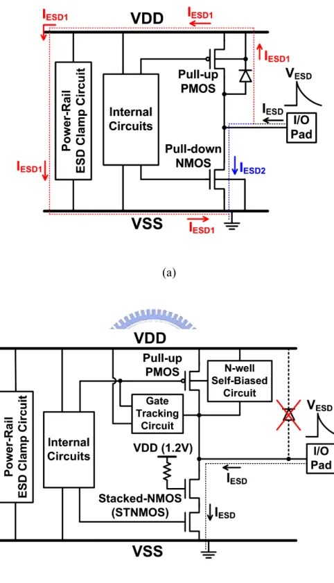
The ESD protection design of I/O pad cooperating with power-rail ESD clamp circuit is shown in Fig. 1.4(a), where a PS-mode ESD pulse is applied to the I/O pad. The ESD current paths (IESD), including IESD1 and IESD2, along the traditional CMOS output buffer are also illustrated by the dashed lines in Fig. 1.4(a), where most of ESD current (IESD1) is discharged through the parasitic diode of the PMOS and the VDD-to-VSS ESD camp circuit to ground. Therefore, the traditional CMOS output buffer can sustain a higher ESD stress with cooperation of active power-rail ESD clamp circuit. But, due to the leakage current issue in
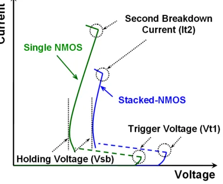
the mixed-voltage I/O circuits, there is no diode connected from the I/O pad to VDD power line in the mixed-voltage I/O circuits. Without the diode connected from the I/O pad to VDD in the mixed-voltage I/O circuits, the ESD current at I/O pad under PS-mode ESD stress cannot be discharged from the I/O pad to VDD power line, and cannot be discharged through the additional VDD-to-VSS ESD clamp circuit. Therefore, the power-rail ESD clamp circuit did not help to pull up ESD level of the mixed-voltage I/O pad under the PS-mode ESD stress. The ESD current path in the mixed-voltage I/O circuits with power-rail ESD clamp circuit under PS-mode ESD stress in illustrated in Fig. 1.4(b). Such ESD current at the I/O pad is mainly discharged through the stacked-NMOS by snapback breakdown. Besides, comparing the single NMOS and the stacked-NMOS in the high-current snapback region, the stacked-NMOS will have a higher trigger voltage (Vt1), a higher snapback holding voltage (Vsb), slower turn-on speed, and a lower secondary breakdown current (It2), as shown in Fig. 1.5. Therefore, such mixed-voltage I/O circuits with stacked-NMOS often have much lower ESD level under the PS-mode ESD stress, as compared to the traditional I/O circuits with a single NMOS [22], [23].In addition, without the diode connected from the I/O pad to VDD, the mixed-voltage I/O circuit also has a lower ESD level for I/O pad under PD-mode ESD stress. The absence of the diode between I/O pad and VDD power line in the mixed-voltage I/O circuits will seriously degrade ESD performance of the I/O pad under the PS-mode and PD-mode ESD stresses. By using extra process modification such as ESD implantation, the ESD robustness of stacked-NMOS device can be further improved [24], [25], but the process complexity and fabrication cost are increased. In addition, the induced high voltage on the gate of top NMOS transistor under ESD stress will cause high-current crowding effect in the channel region to seriously degrade ESD robustness of stacked-NMOS device in the mixed-voltage I/O circuits [26]. Therefore, effective ESD protection design without increasing process complexity is strongly requested by the mixed-voltage I/O circuits in the scaled-down CMOS processes.
One of the mixed-voltage circuit applications, such as the interface in ADSL which has input signals with voltage levels higher than VDD and lower than VSS, is shown in Fig. 1.6 The traditional on-chip ESD protection circuits are not suitable for such mixed-voltage interfaces. The ESD diode Dp (Dn) will be forward biased when the input signal levels are higher than VDD (lower than VSS). This ESD protection circuit will cause current leakage between the chips of the mixed-voltage I/O interface. Moreover, traditional on-chip ESD protection with NMOS/PMOS will also cause the same leakage issue and suffer the gate-oxide reliability issue when the over-VDD or under-VSS external signals reach to the
input pad. To meet such mixed-voltage I/O interface, the SCR device with floating P-well structure in an N-substrate CMOS process had been used as on-chip ESD protection device [27]. However, the SCR device with a floating well structure is very sensitive to latchup [28], [29]. The mixed-voltage I/O interfaces in the system applications often have serious overshooting or undershooting signal transition, which could trigger on the SCR device in the ESD protection circuit of I/O pad to induce latchup troubles to the chip [27].
1.3 Issue of High-Voltage CMOS ICs
High-voltage (HV) CMOS process has been widely used in LCD driver circuits, telecommunication, power switch, motor control systems, etc [30]. In the smart-power technology, high-voltage MOSFET, silicon controlled rectifier (SCR) device, or bipolar junction transistor were used as on-chip electrostatic discharge (ESD) protection devices [31]–[38]. Some ESD protection designs used the lateral or vertical bipolar transistors as ESD protection devices in smart power technology [36], [37]. However, fabrication cost and process complexity are increased by adding bipolar modules into the high-voltage CMOS process. The high-voltage MOSFET was often used as the ESD protection device because it can work as both of output driver and ESD protection device simultaneously in the high-voltage CMOS ICs. With an ultra-high operating voltage, the ESD robustness of high-voltage MOSFET is quite weaker than that of low-voltage MOSFET [31]–[38]. To increase ESD robustness, the conventional design with large device dimension still suffers the non-uniform current distribution among the device. The HV NMOS has the extremely strong snapback phenomenon during ESD stress, which often results in non-uniform turn-on variation among the multi-fingers of HV NMOS [39]. To overcome the problem of non-uniform turn-on phenomenon, the gate-coupling technique was applied to the HV NMOS [32], [33]. However, the gate of HV NMOS must be in series with a large resistor, which occupies a large layout area. Hence, how to improve the ESD robustness of HV NMOS with a reasonable silicon area is indeed an important reliability issue in HV CMOS technology.
In some specific applications, such as the driver IC for vacuum fluorescent display (VFD) [40] in automotive instrumentation [41], only high-voltage PMOS (HVPMOS) is provided in a given CMOS process which is developed by adding a few additional masks and process steps into the low-cost low-voltage CMOS process. To reduce the fabrication cost, no high-voltage NMOS is used in such specific VFD driver IC. For safety concerns in
automotive electronics, the ESD robustness was often requested much higher than that of consumer electronics products. Thus, an additional protection device is necessary in the high-voltage I/O pin to sustain a high enough ESD robustness of the VFD driver IC for safe automotive applications.
1.4 Thesis Organization
To overcome the ESD design constraints in mixed-voltage I/O interfaces, and high-voltage CMOS process, the novel on-chip ESD protection designs are developed and verified in this thesis.
This thesis contains seven chapters. Chapter 1 presents the basic design concept of ESD protection design for commercial IC products in CMOS technology. Moreover, ESD protection design for mixed-voltage I/O interfaces should be concerned about the gate-oxide reliability issue and leakage current path. ESD protection design for high-voltage CMOS process should be concerned about the quite weak ESD robustness due to the ultra-high operating voltage.
In chapter 2, presents an overview on the design concept and circuit implementations of the ESD protection designs for mixed-voltage I/O interfaces without using the additional thick gate-oxide process. To improve ESD level of the mixed-voltage I/O circuits, the ESD protection design without increasing the process complexity is strongly requested by the mixed-voltage I/O circuits in consumer IC products. Such ESD protection design in the mixed-voltage I/O circuits still meets the gate-oxide reliability constraints, and needs to prevent the undesired leakage current paths during normal circuit operating condition. Under ESD stress condition, the ESD protection circuit should be quickly triggered on to discharge ESD current.
In chapter 3, presents a new ESD protection design with the low-voltage-triggered PNP (called as LVTPNP) device to protect the I/O interfaces with input voltage levels higher than VDD or lower than VSS. Comparing to the traditional PNP device in CMOS process, the new proposed LVTPNP with a low breakdown voltage, by avalanche breakdown across the P+/N-well or N+/P-sub junctions, provides effective discharging path to protect the mixed-voltage I/O interfaces against ESD stresses. Under normal circuit operation conditions, the LVTPNP device is kept off without causing current leakage between the chips. Furthermore, layout optimization on the LVTPNP device to increase its ESD robustness per
silicon area has been also studied. The multi-finger layout style is used to improve ESD robustness of the LVTPNP device. Moreover, the input stage of ADSL protected by the LVTPNP device has been practically implemented in a 0.25-μm salicided CMOS process to achieve a better ESD robustness.
In chapter 4, presents a new ESD protection scheme with an ESD_BUS and a high-voltage-tolerant ESD clamp circuit, which is designed to protect the mixed-voltage I/O interfaces against ESD stresses without suffering the gate-oxide reliability issue. The proposed high-voltage-tolerant ESD clamp circuit, which combines the stacked-NMOS of 1.2-V gate oxide with the substrate-triggered technique, is designed to protect the 1.2/2.5 V mixed-voltage I/O interfaces. This high-voltage-tolerant ESD clamp circuit has higher ESD robustness and a faster turn-on speed, which has been successfully verified in a 0.13-μm 1.2-V CMOS process.
In chapter 5, presents a new ESD protection structure with the embedded high-voltage p-type SCR (HVPSCR) into the high-voltage PMOS device to protect the vacuum fluorescent display (VFD) in automotive instrumentation. Only an additional N+ diffusion is added into the HVPMOS to form the HVPSCR for ESD protection. The HVPSCR device structure can greatly improve HBM ESD robustness of the VFD driver IC up to 8kV in the specific 0.5-µm high-voltage CMOS process for automotive electronics applications without suffering latchup issue.
In chapter 6, presents ESD robustness of MOSFETs in a 40-V CMOS process with or without drift implant. In addition, the layout spacing from the drain diffusion to polygate is split to find its dependence on ESD robustness. To improve ESD robustness of HV NMOS in a limit layout area, a specific structure of HV n-type SCR (HVNSCR) can be built in the HV NMOS by replacing part of the drain region with P+ diffusion. ESD robustness of HVNSCR is also verified with or without the N-drift implant under different layout spacings from the drain region to polygate. All test chips have been fabricated in a 0.35-μm 40-V CMOS technology.
Finally, the main results of this thesis are summarized in chapter 7. Some suggestions for the future works are also addressed in this chapter.
(a) (b)
(c) (d)
Fig. 1.1 The four pin-combination modes for ESD test on an IC product: (a) positive-to-VSS (PS-mode), (b) negative-to-VSS (NS-mode), (c) positive-to-VDD (PD-mode), and (d) negative-to-VDD (ND-mode).
(a)
(b)
Fig. 1.3 Typical circuit diagrams for (a) the traditional CMOS I/O buffer, and (b) the mixed-voltage I/O circuits with the stacked-NMOS and the N-well self-biased PMOS.
(a)
(b)
Fig. 1.4 The ESD current paths of (a) the traditional I/O pad with power-rail ESD clamp circuit, and (b) the mixed-voltage I/O pad with power-rail ESD clamp circuit, under the positive-to-VSS (PS-mode) ESD stress. The ESD current paths are indicated by the dashed lines.
Fig. 1.5 The I-V curves in high-current region of single NMOS and stacked-NMOS.
Fig. 1.6 The input signals with voltage levels higher than VDD and lower than VSS in some mixed-voltage I/O interfaces.
CHAPTER 2
OVERVIEW ON ESD PROTECTION DESIGN
FOR MIXED-VOLTAGE I/O CIRCUITS
ESD protection design for mixed-voltage I/O interfaces has been one of the key challenges of SOC implementation in nanoscale CMOS processes. The on-chip ESD protection circuit for mixed-voltage I/O interfaces should meet the gate-oxide reliability constraints and prevent the undesired leakage current paths. In this chapter, an overview on the design concept and circuit implementations of ESD protection designs is presented for mixed-voltage I/O interfaces with only low-voltage thin-oxide CMOS transistors. The ESD design constraints in mixed-voltage I/O interfaces, the classification, and analysis of ESD protection designs for mixed-voltage I/O interfaces are presented and discussed.
2.1 Substrate-Triggered Stacked-NMOS Device
The snapback operation of the parasitic n-p-n BJT in the stacked-NMOS structure can be controlled by its substrate potential. The substrate-triggered technique [42] can be used to generate the substrate current (Isub) in ESD protection circuits. With the substrate-triggered current (Itrig), the trigger voltage of the stacked-NMOS device in mixed-voltage I/O circuits can be reduced for more effective ESD protection.
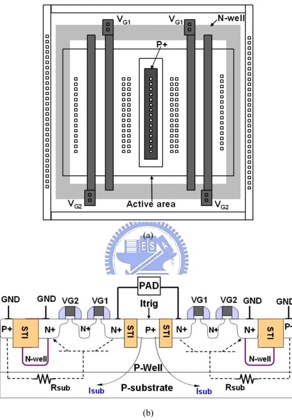
The finger-type layout pattern and the corresponding cross-sectional view of the substrate-triggered stacked-NMOS device are shown in Figs. 2.1(a) and 2.1(b), respectively. As shown in the layout top view, an additional p+ diffusion is inserted into the center drain region of stacked-NMOS device as the substrate-triggered node. The trigger current is provided by the substrate-triggered circuit. An n-well structure is further diffused under the source region, which is also surrounding the whole device, to form a higher equivalent substrate resistance (Rsub) for improving turn-on efficiency of the parasitic lateral BJT in the stacked-NMOS device. The substrate-triggered circuit should be designed to avoid electrical
overstress on the gate oxide and to prevent the undesired leakage current paths during normal circuit operating condition. During ESD stress condition, the substrate-triggered circuit should generate large enough trigger current to effectively improve the turn-on efficiency of parasitic n-p-n BJT in stacked-NMOS device.
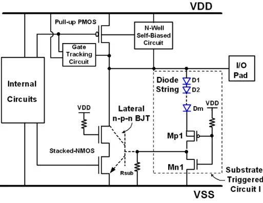
The substrate-triggered circuit I for stacked-NMOS device in the mixed-voltage I/O circuits is shown in Fig. 2.2 [43]. The substrate-triggered circuit I is composed of the diode string, a PMOS Mp1, and an NMOS Mn1, to provide the substrate current for triggering on the parasitic n-p-n BJT in the stacked-NMOS device during ESD stress. Under normal circuit operating condition, the turn-on voltage of the substrate-triggered circuit roughly equals to Vpad ≧ Vstring(I)+|Vtp|+VDD, where Vstring(I) is the total voltage drop across the diodes and Vtp is the threshold voltage of the PMOS. To satisfy the requirement in the 2.5V/3.3V mixed-voltage application, the number of the diodes in the diode string should be adjusted to make the turn-on voltage greater than 3.3V. When a 3.3-V input voltage is applied at I/O pad, Mp1 is kept off, and the local substrate of the stacked NMOS is biased at VSS by the turned-on Mn1. With the diode string to block the 3.3-V input voltage at the I/O pad, the Mp1 with thin gate oxide has no gate-oxide reliability issue under normal circuit operating condition. The Mp1 in conjunction with the diode string is used to reduce the leakage current through the substrate-triggered circuit in normal operating condition. If a lower input leakage is desired, the numbers of the diodes in the diode string should be increased. Under PS-mode ESD stress condition, the gate of the Mp1 has an initial voltage level of ~0V, while the VSS pin is grounded but the VDD pin is floating. The substrate-triggered circuit will provide the trigger current flowing through the diode string and the Mp1 into the p-substrate, when Vpad ≧Vstring(I)+ |Vtp|. The trigger current provided by the substrate-triggered circuit is determined by the diode string and the size of Mp1. Once the parasitic n-p-n BJT in the stacked-NMOS device is triggered on, the ESD current will be discharged from the I/O pad to VSS.
Another substrate-triggered circuit II for stacked-NMOS device in the mixed-voltage I/O circuits is shown in Fig. 2.3 [44]. The substrate-triggered circuit II is composed of the PMOS Mp1, PMOS Mp2, NMOS Mn1, and NMOS Mn2, to provide the substrate current for triggering on the parasitic n-p-n BJT in the stacked-NMOS device during ESD stress. In the 2.5V/3.3V mixed-voltage IC application, the gates of Mp1 and Mp2 are biased at 2.5-V VDD supply through a resistor Rd under normal circuit operating condition. When the input voltage transfers from 0V to 3.3V at the I/O pad, the gate voltage of Mn1 could be increased through the coupling capacitor C. However, the Mn2 and Mp2 can clamp the gate voltage of
Mn1 between VDD-Vtn and VDD+|Vtp|, where Vtn is the threshold voltage of NMOS. Once the gate voltage of Mn1 is over VDD+|Vtp|, the Mp2 will turn on to discharge the over-coupled voltage and to keep the gate voltage within VDD+|Vtp|. Since the upper boundary on the gate voltage of Mn1 is within VDD+|Vtp|, the source voltage of Mp1 is clamping below VDD, which keeps the Mp1 always off under normal circuit operation condition. The Mn2 and Mp2 can further clamp the gate voltage of Mn1 to avoid gate-oxide reliability issue in the substrate-triggered circuit, even if the I/O pad has a high input voltage level. Under PS-mode ESD-stress condition, the gates of Mp1 and Mp2 have an initial voltage level of ~0V, while the VSS pin is grounded but the VDD pin is floating. The positive ESD transient voltage on the I/O pad is coupled through the capacitor C to the gate of Mn1. In this situation, both of the Mn1 and Mp1 are operated in the turned-on state. Therefore, the substrate-triggered circuit II will conduct some ESD current flowing from I/O pad through Mn1 and Mp1 into the p-substrate. The trigger current provided by the substrate-triggered circuit II is determined by the size of Mn1, Mp1, and the capacitor C. Once the parasitic n-p-n BJT in the stacked-NMOS device is triggered on, the ESD current can be mainly discharged from the I/O pad to VSS.
Both two substrate-triggered designs can significantly reduce the trigger voltage and ensure effective ESD protection for the mixed-voltage I/O circuits. By using such substrate-triggered designs, the gates of stacked-NMOS in the mixed-voltage I/O circuits can be fully controlled by the pre-driver of I/O circuits without conflict to the ESD protection circuits. The main ESD discharge device is the parasitic n-p-n BJT in the stacked-NMOS device. Therefore, the ESD robustness of mixed-voltage I/O circuits can be effectively improved without occupying extra silicon area to realize the additional stand-alone ESD protection device into the mixed-voltage I/O cells.
2.2 Extra ESD Protection Device Between I/O Pad and VSS
To improve ESD level of the mixed-voltage I/O circuits, the extra ESD device was added between I/O pad and VSS power line [45], [46]. The ESD current at the I/O pad under PS-mode ESD stress is designed to be directly discharged through this additional ESD device to the grounded VSS. The ESD current at the I/O pad under the PD-mode ESD stress can be discharged through this ESD device to VSS power line, and then through the parasitic diode of power-rail ESD clamp circuit to the grounded VDD.
One ESD protection design with the additional substrate-triggered lateral n-p-n BJT device has been used to protect the mixed-voltage I/O circuits in a fully salicided, 0.35-μm, thin-epi CMOS process [45]. The ESD protection design with substrate-triggered circuit and the lateral n-p-n BJT device for the mixed-voltage I/O circuits is re-drawn in Fig. 2.4(a). The substrate-triggered circuit should meet the design constraints for providing effective ESD protection to the mixed-voltage I/O circuits, but without suffering the gate-oxide reliability issue. In this design, the substrate-triggered circuit is mainly composed of the diode string and a PMOS Mp1 to provide the substrate current for triggering on the lateral n-p-n BJT during ESD stress. A positive feedback network is formed with Mp2, Mn1, and R1, which maintains Mp1 in a highly conductive state to provide the substrate current during ESD stress. Moreover, to improve the turn-on efficiency of lateral n-p-n BJT device in a thin-epi CMOS process with much smaller substrate resistance (Rsub), the device structure of lateral n-p-n BJT is specifically designed in Fig. 2.4(b). The lateral n-p-n BJT device consists of an n+ diffusion (emitter), an n-well (collector), and a p+ diffusion as its base. A dummy gate is formed between the p+ base and n+ emitter regions. The collector n-well encloses a portion of the p+ base region. In this design, the HBM ESD level of the mixed-voltage I/O circuits has been verified greater than 2kV in a fully-salicided thin-epi CMOS process.
Another ESD protection design, by using the additional stacked-NMOS triggered silicon controlled rectifier (SNTSCR), has been reported to protect the mixed-voltage I/O circuits [46]. The ESD protection design with the additional SNTSCR device for protecting the mixed-voltage I/O circuits is shown in Fig. 2.5(a). The device structure of SNTSCR and the corresponding ESD detection circuit are shown in Fig. 2.5(b). The ESD detection circuit, designed by using the gate-coupled technique with consideration of the gate-oxide reliability issue, is used to provide suitable gate bias to trigger on the SNTSCR device under ESD stress condition. On the contrary, this ESD detection circuit must keep the SNTSCR off when the IC is under normal circuit operating condition. During normal circuit operating condition, the Mn3 in Fig. 2.5(b) acts as a resistor to bias the gate voltage (Vg1) of Mn1 at VDD. But, the gate of Mn2 is grounded through the resistor R2 and Mn4. So, all the devices in the ESD protection circuit can meet the electrical-field constraint of gate-oxide reliability under normal circuit operating condition. Under PS-mode ESD stress condition, the Mp1 is turned on but Mn3 is off since the initial voltage level on the floating VDD line is ~0V. The capacitors C1 and C2 are designed to couple ESD transient voltage from the I/O pad to the gates of Mn1 and Mn2, respectively. The coupled voltage should be designed greater than the threshold voltage of NMOS to turn on Mn1 and Mn2 for triggering on the SNTSCR device,
before the devices in the mixed-voltage I/O circuit are damaged by ESD stress. With the gate-coupled circuit technique, the trigger voltage of SNTSCR can be significantly reduced, so the SNTSCR can be quickly triggered on to discharge ESD current. By changing the connection of the ESD protection circuit from the I/O pad to the floating n-well of the pull-up PMOS in the mixed-voltage I/O circuit, the SNTSCR device can have a high enough noise margin to the overshooting glitch on the I/O pad, during the normal circuit operating condition. From the experimental results in a 0.35-μm CMOS process, the HBM ESD level of the mixed-voltage I/O circuits with this ESD protection design has been greatly improved up to 8kV, as compared with that (~2kV) of the original mixed-voltage I/O circuits with only stacked NMOS device.
2.3 Extra ESD Protection Device Between I/O Pad and VDD
To improve ESD level of the mixed-voltage I/O circuits, the extra ESD device was added between I/O pad and VDD power line [47]–[49]. The ESD current at the I/O pad under PS-mode ESD stress is designed to be discharged through this additional ESD device to VDD power line, and then through the power-rail ESD clamp circuit to the grounded VSS. The ESD current at the I/O pad under the PD-mode ESD stress can be directly discharged through this additional ESD device to the grounded VDD.
Because the diode in forward-biased condition can sustain much higher ESD current, the diode string has been used for protecting the mixed-voltage I/O circuits [47], [48], or used to realize the power-rail ESD clamp circuit [50]. The ESD protection design with the diode string connected between the I/O pad and VDD power line for the mixed-voltage I/O circuits is shown in Fig. 2.6. The number of diodes in the diode string is determined by the voltage difference between the maximum input voltage at I/O pad and the VDD supply voltage. To reduce the turn-on resistance from I/O pad to VDD during ESD stress, the area of such diodes has to be scaled up by the number of the diodes in stacked configuration. The major concern of using the diode string for ESD protection in the mixed-voltage I/O circuits is the leakage current. While the mixed-voltage I/O circuit is operating at a high-temperature environment with a high-voltage input signal, the forward-biased leakage current from the I/O pad to VDD through the stacked diodes could trigger on the parasitic vertical p-n-p BJT devices in the diode string. The Darlington bipolar amplification of these parasitic p-n-p BJT devices in the diode string will induce a large leakage current into the substrate. In Fig. 2.6, an additional
snubber diode (SD) was used to reduce the leakage current due to the Darlington bipolar amplification in the diode string [47], [48].
Another ESD protection design, by using the gated p-n-p BJT as the additional ESD device connected between I/O pad and VDD, has been designed to protect the mixed-voltage I/O circuits [49], as that shown in Fig. 2.7. In this ESD protection design, the PMOS Mp1 acting as ESD clamp device should be kept off to avoid the leakage current path during normal circuit operating condition. Under PD-mode ESD stress condition, the parasitic lateral p-n-p BJT in the device structure of Mp1 is turned on to discharge ESD current. In the 3.6V/5V mixed-voltage IC application, when the input voltage at I/O pad is 0V, the n-well voltage and gate voltage of Mp1 is clamped at VDD (3.6V) through the turn-on of Mp2 and Mp4. When the input voltage at I/O pad is 5V, the n-well voltage of Mp1 is maintained at 5-Vd (where Vd is the cut-in voltage of the parasitic drain-to-well diode), and the gate voltage of Mp1 is clamped at 5V through the turn-on of Mp3. Therefore, this design can meet the gate-oxide reliability constraints without leakage current path from I/O pad to VDD during normal circuit operating condition. Under ESD stress condition, the parasitic lateral p-n-p BJT in Mp1 is turned on to discharge ESD current by avalanche breakdown. Such a gated p-n-p BJT should be designed to effectively clamp the overstress ESD pulse without causing ESD damage in the mixed-voltage I/O circuits.
2.4 ESD Protection Design with ESD Bus
The ESD protection scheme by using the additional ESD bus for the IC with power-down-mode application has been reported in [51]. Such design concept with ESD bus can be used to form the ESD protection network for the mixed-voltage I/O circuits, as shown in Fig. 2.8. The additional ESD bus line is realized by a wide metal line in CMOS IC [51], [52]. To save layout area, the ESD bus can be realized by the different metal layer, which overlaps the VDD power line. The ESD bus is not directly connected to an external power pin, but initially biased to VDD through the diode D1 in Fig. 2.8. The diode D1 connected between the VDD power line and ESD bus is also used to block the leakage current path from the I/O pad to VDD during normal circuit operating condition with a high-voltage input signal. The diode Dp is connected between I/O pad and ESD bus, whereas the diode Dn is connected between VSS power line and I/O pad. One (the first) power-rail ESD clamp circuit is connected between VDD power line and VSS power line. Another (the second) power-rail
ESD clamp circuit is connected between the ESD bus and VSS power line. The second power-rail ESD clamp circuit connected between ESD bus and VSS power line should be designed with high-voltage-tolerant constraints without suffering the gate-oxide reliability issue. The ESD current at the I/O pad under PS-mode ESD stress can be discharged through the diode Dp to the ESD bus, and then through the second power-rail ESD clamp circuit to the grounded VSS. The ESD current at the I/O pad under the PD-mode ESD stress can be discharged through the diode Dp to the ESD bus, the second power-rail ESD clamp circuit to VSS power line, and then through the parasitic diode of the first power-rail ESD clamp circuit to the grounded VDD. With the turn-on-efficient power-rail ESD clamp circuits, high ESD level for the mixed-voltage I/O circuits can be achieved by this ESD protection scheme with ESD bus. Here, the design key point is how to design such a high-voltage-tolerant power-rail ESD clamp circuit with only low-voltage thin-oxide CMOS devices.
2.5 Special Applications
For high-frequency and analog circuit applications, the high-voltage-tolerant ESD protection design should meet the constraint of low parasitic capacitance. The traditional analog ESD protection with double diodes connected between I/O pad and VDD/VSS power lines [53] cannot meet the high-voltage tolerant requirement. A high-voltage-tolerant ESD protection design, by using the forward-biased diode in series with the stacked-NMOS device, has been reported for analog ESD protection to reduce the input parasitic capacitance [54], as shown in Fig. 2.9. The equivalent capacitance of analog pin in this design is approximate the junction capacitance of D1 plus the junction capacitance of D2. The diodes D1 and D2 can be drawn with small layout area, because the ESD current is discharged through these diodes under forward-biased condition. Therefore, the total parasitic input capacitance seen by the analog pin was reduced. The gates of Mn1 and Mn3 are connected to VDD to meet the gate-oxide reliability. The gates of Mn2 and Mn4 are grounded by the dynamic-floating-gate technique [55] to improve turn-on uniformity among the multiple fingers of the stacked NMOS device. The ESD current at the I/O pad under PS-mode ESD stress can be discharged through the diode D1 and the parasitic n-p-n BJT of stacked-NMOS (Mn3 and Mn4) to the grounded VSS. The ESD current at the I/O pad under PD-mode ESD stress can be discharged through the diode D1 and the parasitic n-p-n BJT of stacked-NMOS (Mn1 and Mn2) to the grounded VDD. Because the ESD current is discharged through the stacked-NMOS device by