國 立 交 通 大 學
光 電 工 程 研 究 所
碩士論文
不同厚度之非極性"a"平面氮化銦鎵多重量子井結構
之光學特性
Optical characteristics of a-plane InGaN/GaN
multiple quantum wells with different well widths
研究生:高潤琪
指導教授:郭浩中 教授
盧廷昌 教授
不同厚度之非極性"a"平面氮化銦鎵/氮化鎵多重量子井之光學特性
Optical characteristics of a-plane InGaN/GaN multiple quantum wells
with different well widths
研究生:高潤琪 Student: Run-Ci Gao 指導教授:郭浩中 教授 Advisor: Prof. Hao-Chung Kuo
盧廷昌 教授 Prof. Tien-Chang Lu
國 立 交 通 大 學
光電工程研究所
碩 士 論 文
A Thesis
Submitted to Institute of Electro-Optical Engineering College of Electrical Engineering
National Chiao Tung University in Partial Fulfillment of the Requirements
for the Degree of Master
In
Electro-Optical Engineering
July 2007
不同厚度之非極性"a"平面氮化銦鎵/氮化鎵多重量子井之光學特性
研究生:高潤琪 指導教授: 郭浩中教授 盧廷昌教授 國立交通大學光電工程研究所碩士班摘要
本論文中,我們利用有機金屬氣相沉積磊晶技術成長不同厚度之非極性"a" 平面氮化銦鎵/氮化鎵多重量子井作為研究對象。我們利用光激發螢光(PL)、螢 光激發(PLE)光譜、以及時間解析的光激發螢光(TRPL)光譜技術進行樣品的光學 特性分析。 在室溫PL實驗中,顯示了非極性氮化銦鎵/氮化鎵多重量子井的內建電場並 不影響其位能,且其發光強度隨著量子井厚度由3奈米增加到12奈米而減弱。除 此之外,變溫PL實驗顯示了一個較明顯的載子侷限效應(localization effect) 存在於量子井較厚的樣品中,同時它們在螢光激發光(PLE)實驗中也顯示出較大 的史托克位移(Stokes shift),我們將這樣的現象歸因於銦含量分佈不均勻以及 晶格品質缺陷所造成。成長非極性結構的另一優勢在於極化發光(polarized light emission)的價值,我們所測得的發光極化率大約在60%左右。 另外,時間解析的光激發螢光(TRPL)光譜顯示出量子井厚度差異確實導致載 子輻射復合速度不同,在最薄3奈米的樣品中有最佳的載子捕陷以及放光效率, 這和不同厚度樣品在成長過程中所導致的銦含量不均程度及侷限深度差異有很 大關係。 最後,利用陰極激發光(CL)和共焦顯微影像,進一步證實了樣品發光的均勻 性以及強度隨著量子井厚度增加而逐漸退化變差的現象。Optical characteristics of a-plane InGaN/GaN multiple quantum
wells with different well widths
Student : Run-Ci Gao Advisor: Prof. Hao-Chung Kuo Prof. Tien-Chang Lu
Institute of Electro-Optical Engineering
National Chiao Tung University
Abstract
In this thesis, a-plane InGaN/GaN multiple quantum wells with different widths from 3 to 12 nm were grown on r-plane sapphire by metal organic chemical vapor deposition for investigation. We utilized several methods including photoluminescence (PL), photoluminescence excitation (PLE), and time-resolved photoluminescence (TRPL) to investigate the optical characteristics of our samples.
The PL experiments revealed that the PL emission intensity would decrease with increasing the well width of the samples from 3 to 12 nm. Meanwhile, the power dependent PL measurement indicated no apparent emission peak shift for all samples due to no built-in electric field in a-plane MQWs. Moreover, the temperature dependent PL reveals that a more apparent localization effect exist in the sample with a thicker well width which is most likely due to more serious indium fluctuations or worse crystalline quality in the MQWs. In PLE experiment, a larger Stokes shift and a broaden PLE spectrum are observed when the well width becomes wider. In-plane
polarization effect of a-plane InGaN/GaN MQWs emission was also investigated, which pointed out an average polarization degree ρ from our samples is about 60%.
The TRPL experiments were carried out to further compare the differences of carrier dynamics between all our samples. Low temperature TRPL indicated that the shorter radiative lifetime could be obtained in the samples with thinner well width. The decay time corresponding to different energies of PL spectra at 9 K were analyzed, which indicated that the decay time on the lower energy side of the PL peaks was longer than that on the higher energy side due to the inhomogeneously broadened localization effect in our samples. In the temperature dependent TRPL, shorter τloc and smaller dτloc/dT prove that more effective capturing of excitons due
to larger Eloc and shorter radiative lifetime of localized excitons are presented in
thinner well width samples.
Eventually, the results of cathodoluminescence and micro-PL scanning images further verified the more uniform and stronger luminescence intensity distribution observed for the samples with thinner quantum wells, indicating that the epitaxial condition and In fluctuation during the quantum well growth shall dominate the optical characteristics of the nonpolar a-plane MQWs. These results should provide a useful guidance for fabrication of light emitting devices using a-plane InGaN/GaN MQW structures.
致謝
終於還是到了畢業的時候,轉眼的時光飛逝在這一刻特感受特別地深,碩士 班兩年的生活因為有很多人默默地支持、鼓勵,我才能夠走到今天。首先,特別 感謝實驗室三位老師:王老師,郭老師,盧老師,我很幸運,同時擁有三位學經 歷背景豐碩傑出的老師指導,你們對研究的堅持、對實驗室的付出、以及對學生 的用心是我得以順利完成研究的最大支持,相信未來,實驗室在老師們的帶領 下,會不斷向更傑出、突破的研究成果邁進。 謝謝宗憲學長的帶領,你是最照顧學弟妹的學長,不論在研究上還是生活 上,很開心這兩年能夠和你一起學習,祝福學長順利赴國外學習,收穫滿滿,順 利畢業。 謝謝亞銜學長的經驗分享,謝謝小賴學長的好吃包子,謝謝姚忻宏學長常開 車載大家去吃好料,謝謝游敏、意偵學姊的指導與陪伴,謝謝你們陪我走過充滿 歡笑的碩一。 謝謝小強學長,一直對你研究上的表現佩服,也謝謝你對我的關心以及待人 處世上的經驗分享,你真的一點也不嫩,哈。謝謝小朱學長,很喜歡聽你講笑話, 沒等到你的八卦是我畢業的遺憾。謝謝乃方學姊,和你聊天總是有爆點,俊榮學 長,謝謝你解決我模擬上的疑問,謝謝明華學長,和你討論實驗很有收穫,謝謝 清華學長、士偉學長,實驗室有你們,相信會更加茁壯。 還有,我的好同學們;碩均,祝福你的博班順利愉快,家璞,你對上帝的堅 信力量感染了我,謝謝有你這個好同學,和你一起上課、作實驗討論很開心,等 你好消息:) 金門,我找不到詞形容你的體貼,謝謝你常常讓我感到溫暖與窩心, 孟儒,你總是認真又努力,祝你工作、感情都順利,卓奕,沒機會見識你游泳的 英姿了,祝福你在群創如魚得水,瑞農,你對理論研究的堅持和付出很讓人敬佩, 祝福你在國外找到自己的一片天。可愛的碩一學弟妹們,小恬恬,你總是體貼又認真,謝謝你陪我走過碩二的 生活,有機會帶你一起做實驗是一件讓人開心的事:)伯駿、柏源、家銘、晁恩、 子維、士嘉、建達、恕帆、柏孝、承恩,實驗室的未來就靠你們了,祝你們實驗 順利,研究愉快。 還有,我的大學好同學們,謝謝你們,有你們在的新竹就如同高雄一樣快樂, 一樣單純,開心,祝大家飛黃騰達,唸書的研究順利,工作的賺大錢。 謝謝 mat,這兩年有你陪伴,我很幸福,謝謝你,要一起加油:)最後,謝 謝我的家人,感謝你們一直與我同在,我愛你們。
Content
摘要...i
Abstract ………ii
致謝……… iv
Content………..vi
List of tables ………viii
List of figures……….ix
Chapter 1 Introduction
1.1 The development of III-Nitride nanostructure from c-plane to a-plane………….11.2 Motivation ……….………..4
Chapter 2 Characteristics of III-Nitride quantum well structure
2.1 Quantum confinement effect in semiconductor nanostructure………62.2 The localization effect in quantum well structure………8
2.3 The basic concept of nonpolar nanostructure……….…..9
2.4 In-plane light polarization effect in nonpolar nanostructure………11
Chapter 3 Sample growth and experiment setup
3.1 Sample growth and HRXRD quantification………...………143.2 Photoluminescence (PL)………18
3.3 Photoluminescence excitation (PLE)………20
3.4 Confocal optical image………21
Chapter 4 Optical properties of a-plane InGaN/GaN MQWs (I)
4.1 Introduction………264.2 Photoluminescence spectra of a-plane InGaN/GaN multiple quantum wells 4.2.1 Room temperature photoluminescence………28
4.2.2 Power dependent photoluminescence………...28
4.3 The localization effect of a-plane InGaN/GaN multiple quantum wells 4.3.1 Temperature dependent photoluminescence………30
4.3.2 Photoluminescence excitation……… 35 4.4 In-plane polarization effect of a-plane InGaN/GaN MQWs emission……...37 4.5 Conclusion………39
Chapter 5 Optical properties of a-plane InGaN/GaN MQWs (II)
5.1 Introduction………51 5.2 Time-resolved photoluminescence
5.2.1 Low temperature TRPL……….52 5.2.2 PL decay time as a function of monitored photon energy at 9K……...53 5.2.3 Temperature dependent TRPL………...54 5.3 Confocal optical image………...57 5.4 Conclusion………..59
Chapter 6 Conclusion
6.1 Conclusion………..…………66 6.2 Future work………67
List of tables
Table 3.1.1 The HRXRD measured layer thickness and composition
Table 4.3.1 The fitting results of activation energy for the a-plane InGaN/GaN MQWs with different well width.
List of figures
Fig. 1.1.1 The planar relation and orientation in hexagonal crystal structure Fig. 2.3.1 A schematic energy band diagram of (a) nonpolar quantum well and (b)
polar quantum well under QCSE. Fig. 3.1.1 A schematic drawing of sample structure
Fig. 3.1.2 The specific crystallographic index used in the HRXRD analysis.
Fig. 3.1.3 (a)(b)(c)(d) Experiment and simulation results of HRXRD ω-2θ scans for a-plane InGaN/GaN MQWs.
Fig. 3.2.1 The setup of PL system Fig. 3.3.1 The setup of PLE
Fig.3.4.1 A schematic diagram of the confocal principle [26] Fig. 3.4.2 The confocal microscope experiment setup
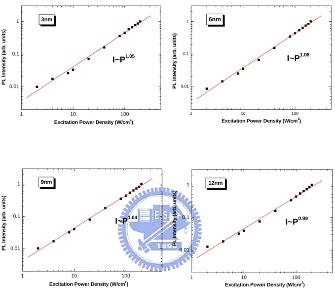
Fig. 4.2.1 (a) Room temperature PL spectra of a-plane InGaN/GaN MQWs with well width ranging from 3 to 12 nm. (b)(c) Normalized PL energy peak and intensity plotted as a function of quantum well width.
Fig. 4.2.2 PL spectrum as a function of the excitation power for a-plane InGaN/GaN MQWs with different well width.
Fig. 4.2.3 The relation between PL intensity and excitation power density for a-plane InGaN/GaN MQWs with different well width.
Fig. 4.3.1 PL spectra as a function of temperature from 20K to 300K for a-plane InGaN/GaN MQWs with different well width.
Fig. 4.3.2 Normalized integrated PL intensity as a function of 1/T for the a-plane InGaN/GaN MQWs with different well width.
Fig. 4.3.3 PL peak energy position as a function of temperature for a-plane InGaN/GaN MQWs with different well width.
different well width.
Fig. 4.4.1 The wurtzite GaN unit cell and the definition of crystal axes.
Fig. 4.4.2 μ-PL spectra of the a-plane InGaN/GaN MOWs for polarization angles between 00 and 3600 in steps of 150.
Fig. 4.4.3 Normalized μ-PL intensity versus the in-plane polarization angle for the a-plane InGaN/GaN MOWs with different well width.
Fig. 4.4.4 Normalized μ-PL spectra for E//c (900) and E⊥c (00) for the a-plane a-plane InGaN/GaN MOWs with different well width.
Fig. 5.2.1 (a) (b) TRPL signals of emission peaks in the a-plane InGaN/GaN MQWs with different well width. (b) Relation between ln[ln(I0/I(t))] and ln(t) for the signal in(a).
Fig. 5.2.2 PL decay time as a function of monitored photon energy at 9K and the fitting data for the a-plane InGaN/GaN MQWs with different well width. Fig. 5.2.3 TRPL signal of a-plane InGaN/GaN MQWs with 12nm well width
measured at various temperature.
Fig. 5.2.4 Schematic diagram of localized exciton system. Excitons are transferred from free/extended states to the localized states. [41]
Fig. 5.2.5 PL lifetime τPL of a-plane InGaN/GaN MQWs with different well width as a function of temperature. The localization lifetimeτloc and nonradiative lifetime at the free/extended states τnr,free estimated from the T-dependent TRPL signal and PL intensity are also plotted.
Fig. 5.2.6 τloc as a function of temperature for the a-plane InGaN/GaN MQWs with different well width.
Fig. 5.3.1 (a) Monochromatic top view CL images and (b) Top view µ-PL confocal images of a-plane InGaN/GaN MQWs with different well widths using optical filter at corresponding peak emission wavelength of different well widths
Chapter 1 Introduction
1.1 The development of III-Nitride nanostructure from c-plane to a-plane
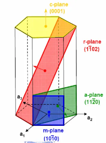
In the past, a lot of process had been made in developing high-quality III-nitride electronic and optoelectronic devices. To date most of the reported laser diodes and light-emitting diodes were grown on sapphire、6H-SiC、or free standing GaN in the [0001] orientation. In such configuration, the [0001] polar axis, resulting from the non-centrosymmetric nature of the wurtzite phase, is aligned along the growth direction. Hence, polarization discontinuities exist along the growth direction and create fixed sheet charges at surfaces and interfaces. The total polarization of III-nitride film consists of spontaneous and piezoelectric polarization contributions. These resulting internal electric fields would bend the potential band and spatially separate electron and hole wavefunctions in potential wells which further reduce the overlap degree of them. Thus, reduced carrier recombination、red-shift emission and decreased internal quantum efficiency are caused. These effects are manifestations of the quantum confined Stark effect (QCSE) and have been thoroughly analyzed for GaN/ (Al,Ga)N quantum wells. [1~2]
Now, nonpolar growth is a promising means of elimination the strong polarization-induced electric fields exist in wurtzite nitride semiconductors because the polar c-axis lies in the QW plane. In a word, it is a way through choosing substrate of different orientation to grow nanostructures that have no polarization electric field
along growth direction in nature. There have been several approaches to realize nonpolar nanostructure, the most common two approaches are growing [1100] oriented m-plane heterostructures on γ-LiAlO2 (100) [3~4] and [11
−
2 0] oriented a-plane heterostructures on r-plane sapphire. [5~7] Planar relation and orientation in hexagonal crystal structure is shown in figure 1.1.1. So far, nonpolar structure has been applied to grow AlGaN/GaN and InGaN/GaN heterostructures.
Although the optical characteristics of polar c-plane heterostructures have been studied extensively [8~9], there are still lots of optical properties of nonpolar heterostructure worth research for assistance of fabrication high efficiency optoelectronic devices. A rash of efforts have been put into nonpolar structure growth approaches and optical properties researches in these years. [10~13] In this thesis, the optical characteristics and carrier recombination mechanisms of well-width dependent a-plane InGaN/GaN multiple quantum wells will be discussed.
1.2 Motivation
Conventional polar (c-plane) InGaN/GaN MQWs have been widely used as active layers for high brightness light-emitting diodes and continuous-wave laser diodes. But one of the most difficult challenges to improve the operation efficiency is its internal electric field as described in section 1.1. Since the non-polar QW band profiles are claimed that unaffected by internal fields, higher internal quantum efficiency and lower threshold current devices are fervently expected.
Theoretically, nonpolar a-plane InGaN/GaN MQWs have potential ability to overcome the QCSE existed in polar systems and to greatly improve device efficiency. However, so far carrier recombination mechanisms and optical characteristics about them are not yet understood well. Thus, in this thesis, we put our efforts to study the optical characteristics of nonpolar a-plane InGaN multiple quantum wells grown on r-plane sapphire by metal organic chemical vapor deposition (MOCVD). Samples with different well thickness ranging from 3 to 12 nm were prepared for comparison. A series of optical experiments were applied not only to get the relations between well width and emission characteristics but also to suggest a probable effect during the growth process of different well width of InGaN/GaN MQW.
The thesis is organized in the following way: In chapter 2, we give some theoretical backgrounds about III-nitride quantum well structure and the
characteristics of nonpolar based nanostructures. The experimental setups and sample structures are stated in chapter 3. In chapter 4 and 5, we present the experiment results and discuss them in detail. Finally, we give a brief summary of the study in this thesis.
Chapter 2 Characteristics of III-Nitride quantum well structure
2.1 Quantum confinement effect in semiconductor nanostructure
If we make very small crystals, the optical properties of solids will depend on their size. The size dependence of the optical properties in very small crystals is a consequence of the quantum confinement effect. What "Quantum confinement" means is that when electrons and holes in a semiconductor are restricted in one or two or even three dimensions. For exemple, a quantum dot is confined in all three dimensions, a quantum wire is confined in two dimensions, and a quantum well is confined in one dimension. Therefore, quantum confinement occurs when one or more of the dimensions of a nanostructure is very small so that it approaches the size of an exciton in bulk crystal, called the Bohr exciton radius. [14] In this thesis, we talk about quantum well structure which is a structure where the height is approximately the Bohr exciton radius while the length and breadth in the other two dimensions are relatively free from constraint.
The distance between the electron and the hole is called the effective Bohr radius, aB of the exciton. When the well width is much larger than aB in bulk, the exciton
binding energy will not show evident difference between the well and the bulk, for the excitons feel nearly the same environment as in bulk. As the well width is decreased
to the order or less than the order of aB, the wave functions of electrons and holes
overlap get improved and are confined in the well. This also improves the exciton binding energy.
The Hamiltonian describing the relative motion of the exciton could be written as
H=He(xe)+Hh(xh)+He-h(r)
where He and Hh are the Hamiltonian describing the electron and hole motion
confined in the well. He-h is theHamiltonian includes the kinetic energy part of the
relative motion of the exciton in the Y-Z plane and the Coulomb potential attracting the electron and the hole in the three dimensional form. The x-coordinate of the electron and hole is denoted as xe and xh while r represent the relative position vector
between the electron and the hole. Therefore the eigenvalue solved is given by En= Eexn +Ehxn-Ee-h
where Ee
xn andEhxn is the energy of nth quantum confined state, and Ee-h is the binding energy of exciton defined as positive value. Therefore, the lowest exciton resonance energy associated with the ground state in the quantum well could be written as Eemission = Eg+ Eexn +Ehxn-Ee-h
The resonance energy was sensitive to well width and the monatomic well size fluctuation in the narrower well. The well width dependence of the absorption spectra
is determined by competition between the quantum confinement energy level and the exciton binding energy.
2.2 The localization effect in quantum well structure
Quantum wells based on InGaN and GaN grown on c-plane sapphire have been actively studied over the past several years for light emission. It has been seen that in spite of the substrate mismatch related high dislocation densities, the nanostructures still have reasonable quantum efficiencies in these quantum wells. In conventional light emitters, such a high density of dislocations would severely degrade the radiative efficiency. It is widely accepted that the high luminescence efficiency of polar InGaN-based structures is due to the exciton localization effect. [15~16] Exciton localization effect is thought from a lot of reports to be induced by compositional fluctuation and phase separation observed in InGaN layers. [17~18] Furthermore, the exciton localization effect is influenced by quantum well thickness、indium content and doping level.
Once the clusters like In-rich QD due to compositional fluctuation and phase separation formed in InGaN/GaN quantum wells, they would cause appreciable localization of the electron and hole wavefunctions. As a result of a very high degree
of localization, electrons and holes injected into the InGaN quantum well are unable to reach dislocations. This causes high radiative emission efficiency as most carriers are tapped well in localization states. The effect of indium segregation in InGaN is described by a ratio that indicates the degree of variation of In content in a cluster from pure InN cluster case. A small amount of clustering is able to provide a sufficient number of localized states for this purpose. In absence of such clustering, the carrier wavefunctions are extended into the dislocations.
2.3 The basic concept of nonpolar nanostructure
It was from 1994, the use of InGaN/GaN double heterostructure (DH) in LEDs by Nakamura is thought to reignite the III-V nitride system. People did a lot of work in all aspects to improve the light emission efficiency including the material selection、crystal growth、device manufacture process etc. One of the difficulties hampering further advances in nitride emitters is the presence of large piezoelectric fields in these materials.
InGaN/GaN multiple quantum wells are a widely used material and structure to serve as the active layer in nitride heterostructures for its advantage in easy tuning wavelength through controlling the composition of indium. However conventional
InGaN/GaN quantum wells grown along the crystallographic c-axis exhibit an internal spontaneous and piezoelectric field in the MV/cm range. The spontaneous field is induced from different atoms arrange in one direction parallel with the growth axis while the piezoelectric field is caused by biaxial compressive strain due to the lattice mismatch between InGaN and GaN.
Under such field, electrons and holes are drawn to opposite interfaces of the QW and the spatial separation of wave functions suppresses radiative recombination with respect to nonradiative recombination, diminishing the emission efficiency drastically. The built in piezoelectric field also causes a red-shift emission. All the effects caused by the build in electiric field are called as Quantum Confined Stark Effect (QCSE) [1~2].QCSE becomes severe when the quantum well width gets thicker and indium content is increased. In order to overcome the problem, nonpolar structure was thought as a method to eliminate the built in polarization field. Waltereit and colleagues at the Paul Drude Institute in Berlin first demonstrated the absence of the piezoelectric field in m-plane GaN/AlGaN QWs grown on LiAlO2 substrates [3].
Recently, there have been several approaches to realize nonpolar GaN, m-plane films [19] and M-plane heterostructures [3~4] on γ-LiAlO2(100) as well as a-plane films
[20] and a-plane heterostructures [5~7] on r-plane sapphire.The planar relations in hexagonal crystal structure was shown in figure 1.1.1.
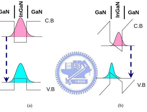
A schematic energy band diagram between nonpolar quantum well and polar c-plane quantum well under QCSE is shown in figure 2.3.1(a) (b). As can been seen, the well potential in the nonpolar nanostructure is not influenced by the built in polarization field and possess a higher wavefunction overlap and emission energy than polar nanostructure. Thus nonpolar is now a chance to improve the light emitting efficiency greatly and make a grand breakthrough in the III-V nitride system development.
2.4 In-plane light polarization effect in nonpolar nanostructure
In addition to the advantage of no internal electric fields in growth direction, nonpolar orientation of the wurtzite crystal structures are also good for polarization-sensitive devices. In contrast to GaN films grown along the polar c-plane direction, do not exhibit any in-plane polarization anisotropy, m- and a-plane GaN films, where the c-axis lies in the film plane, exhibit significant polarization anisotropy in its light emission.
When GaN films are grown on c-plane substrates with similar hexagonal symmetry, there is no linear polarization emission happened under isotropic in-plane strain. However, a GaN film with an m-plane or a-plane orientation experience anisotropic in-plane strain resulted from the inherent lower symmetry of m and a
plane. An in-plane polarization anisotropy has been observed in the PL spectra of GaN/(Al,Ga)N MQWs. [12, 21]
The coordinate system used for the investigation of the polarization properties is x//a[112 0]、y//m[1− 100]、and z//c[0001], the three planes are perpendicular to each − other. Take the m-plane GaN films for example, m-plane strain lifts the symmetry in the x-y plane of the wurtzite crystal and separates the original |X±iY>-like HH and LH states of unstrained WZ-GaN to |X>-like and |Y>-like states. A compressive strain along x induces a dilatation along y so that the energy of the |X>-like state is raised while the |Y>-like state is lowered. Valence bands are reconstituted to |X>-like, |Z>-like, and |Y>-like states in order of decreasing electron energy. Therefore, the valence band structure is altered that the lowest transition energy is totally linearly polarized in the x-direction (E⊥C), while the second lowest transition energy is totally linearly polarized in the z-direction (E║C). The third lowest transition energy which is linearly polarized in the y-direction will not show any PL intensity difference when we put the polarizer in x-z plane to get the polarization information.
The optical polarization anisotropy in GaN films with a nonpolar orientation can be used for polarization-sensitive photodetectors [22] and static as well as dynamic polarization filtering [23]. It has also been applied to achieve polarized emission in (In,Ga)N/GaN light-emitting diodes grown along nonpolar orientations [24].
(a) (b)
Fig. 2.3.1 A schematic energy band diagram of (a) nonpolar quantum well and (b) polar quantum well under QCSE.
C.B
V.B
InGaN
GaN
GaN
C.B
V.B
InGaN
GaN
GaN
Chapter 3 Sample Preparation and Experiment Setup
3.1 Sample growth and HRXRD quantification
All epitaxial films were grown on r-plane sapphire in MOCVD reactor. Trimethylgallium, trimethylindium, and ammonia were the precursors used for sources of Ga, In and N in whole epitaxy process. At first, the r-plane sapphire substrate was treated by thermal annealing at 1090 . Subsequently, a 30 nm ℃ thickness AlN nucleation layer was deposited at 600 . The growth temperature was ℃ ramped up to 1120 to grow a℃ -plane bulk GaN of 2 µm thickness. The MQWs structure was grown at 700 which con℃ sisted of 10 pairs of GaN barriers and InxGa1-xN wells. We controlled different growth time ranging from 1~3 minutes on
growing quantum well to get different active layer thickenss. Finally, the 50 nm capping layer of GaN was deposited. A schematic diagram of sample structure was shown in figure 3.1.1
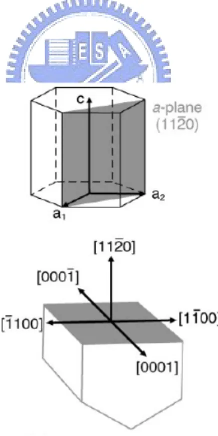
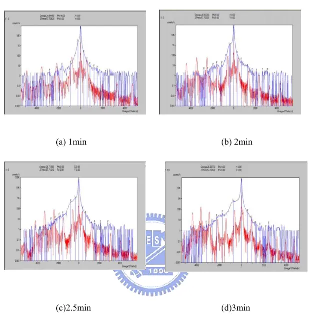
The ω-2θ scan measurements of high resolution x-ray diffraction (HRXRD) made with a Philips MRD X’pert PRO diffractometer using CuKα1 radiation were applied to quantify the quantum well and barrier thicknesses. The In composition could also be made sure. Figure 3.1.2 is a schema of the (112 0) a-plane orientation − which defines the specific crystallographic index used in the HRXRD analysis. The dynamic diffraction simulation shown in figure 3.1.3(a)~(d) models the
peak locations of the HRXRD experimental results. The X-ray diffraction analysis confirmed that the In composition of the quantum well is around 23%, the GaN barrier is around 12 nm thick and the approximate well width for different growing time samples are 3, 6, 9, and 12 nm, respectively. We concluded the HRXRD measured result in table 3.1.1.
Fig. 3.1.1 A schematic drawing of sample structure
Fig. 3.1.2 The specific crystallographic index used in the HRXRD analysis.
10 periods GaN/InGaN MQWs
r-plane Sapphire AlN nucleation layer
Bulk GaN GaN capping layer
(a) 1min (b) 2min
(c)2.5min (d)3min
Fig. 3.1.3 Experiment and simulation results of HRXRD ω-2θ scans for a-plane InGaN/GaN MQWs.
1min 2min 2.5min 3min
In composition 0.23 0.23 0.23 0.23
well
thickness 3.3nm 5.9nm 8.8nm 12.1nm
3.2 Photoluminescence (PL)
Photoluminescence spectroscopy is an un-contact, nondestructive method of examining the electronic structure and optical characteristics of materials. Photoluminescence is the emission of light from a material under optical excitation. It needs an excited light source to induce the emission and the energy of the excited light source should be higher than the band gap energy of the material. Light is directed onto a sample where it is absorbed and electrons in the valence band would get the energy to jump into the conduction band then relatively produce a hole in the valence band. When an excited electron in the conduction band returns back to the valence band, it releases the energy which includes a radiative process and a nonradiative process.
The energy of the emitted light (photoluminescence) relates to the difference in energy levels between two states involved in the transition which are the excited state and the equilibrium state. The intensity of the emitted light is related to the contribution of the radiative process. The intensity and spectral content of a photoluminescence spectrum is a direct inspection of material properties.
When it comes to radiative recombination process in semiconductors, there are many different path it could get through .We can recognized these various transitions by PL emission at low temperature, since low temperature rules out the influence of
thermal energy. Before recombination, an electron and a hole usually form a quasi-particle that is a bound state with Coulomb interaction between them. The quantum of this electronic polarization is called as exciton. The introduction of the exciton was made by Frenkel in 1931.
Generally in semiconductor, a weakly bound e-h pair whose wavefunction propagates more than the lattice spacing is formed and is called as Mott-Wannier exciton (free exciton, FE). [25] Conversely in ionic crystals or molecular crystals, e-h pair is strongly bound at the matrix atom or localized at its neighborhood. This type of exciton is called as Frenkel exciton. (bound exciton, BE).
Stable excitons will only be formed if the attractive potential is sufficient to protect the exciton against collisions with phonons. Mott-Wannier excitons have small binding energy due to their large radius, with typical values of around 0.01eV. Since KBT ~0.025eV at room temperature, where KB is Boltzmann’s constant, these
excitons are only observed clearly at low temperature in many materials. Frenkel excitons, on the other hand, have larger binding energies of the order 0.1-1eV, which makes them stable at room temperature.
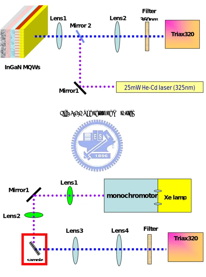
The setup of our PL system is shown in Fig. 3.2.1. The pumping light source was a multi-mode and non-polarized Helium-Cadmium laser operated on 325nm with
20mW. After reflected by three mirrors, the laser light was focus by a lens which focal length was 5cm, to 0.1mm in diameter and the luminescence signal was collected by the same lens. The probed light was dispersed by 0.32 monochromator (Jobin-Yvon Triax-320) equipped with 1800, 1200, and 300 grooves/mm grating and which maximum width of the entrance slits was 1mm. The resolution was controlled in 1nm by selecting 300 grooves/mm grating and slit of 0.1mm. We use long pass filter to avoid the laser coupling with the PL spectrum.
3.3 Photoluminescence Excitation (PLE)
In PL measurement, which is peformed at a fixed excitation energy, the luminescence properties are generally investigated. In PL excitation (PLE) spectroscopy, which is carried out at fixed detection energy, provides mainly information about the absorption properties. Apart from PL experiments, the PLE measurement is a widely used spectroscopic tool for the characterization of optical transitions in semiconductors.
It is very important to note that the PLE experiment also depends strongly on the different carrier relaxation processes that connect the absorbing state to the luminescent state. Nevertheless, in many cases it is difficult to separate the influence of relaxation from that of absorption. The PLE spectrum is strongly influenced by the
relaxation depending on different samples.
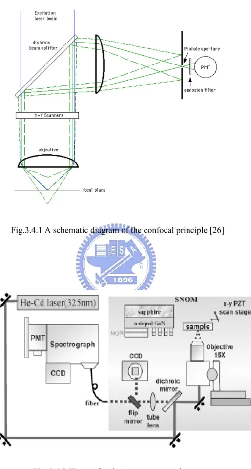
The setup of our PLE system is shown in Fig 3.3.1. Except for the excited light source, the whole light collection setup and spectrometer (Triax320) are the same as PL system.
The pumping source of PLE was Xe lamp with 450W separated by a double-grating monochoramator (Jobin-Yvon Gemini180) and then coupled to samples at an angle about 450 by two focal lenses. We fixed the detection energy
through the spectrometer Triax320, and changed the excitation energy range of Xe lamp to get PLE spectrums. At the exit of the spectrometer Triax 320, a high sensitive Hamamatsu photomultiplier tube (PMT) with GaAs photocathode was placed to detect the luminescence signals.
3.4 Confocal Optical image
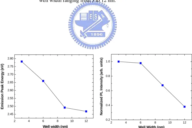
"Confocal" is defined as having the same focus. What this means in the microscope is that the final image has the same focus as or the focus corresponds to the point of focus in the object. The object and its image are "confocal". The microscope is able to filter out the out-of-focus light from above and below the point of focus in the object. Normally when an object is imaged in the fluorescence microscope, the signal produced is from the full thickness of the specimen which does
not allow most of it to be in focus to the observer. The confocal microscope eliminates this out-of-focus information by means of a confocal pinhole situated in front of the image plane which acts as a spatial filter and allows only the in-focus portion of the light to be imaged. Light from above and below the plane of focus of the object is eliminated from the final image. A schematic diagram of the confocal principle is shown in Fig 3.4.1. [26]
Confocal microscopy offers several advantages over conventional widefield optical microscopy, including the ability to control depth of field, elimination or reduction of background information away from the focal plane (that leads to image degradation), and the capability to collect serial optical sections from thick specimens. The basic key to the confocal approach is the use of spatial filtering techniques to eliminate out-of-focus light or glare in specimens whose thickness exceeds the immediate plane of focus. In fact, confocal technology is proving to be one of the most important advances ever achieved in optical microscopy.
The confocal microscope experiment setup is shown in Fig.3.4.2.We chose a 40x objsctive and a 100um fiber to collect the optical signal from the samples that gave a space resolution about 3um. The excitation light source was a multi-mode Helium-Cadmium laser operated on 325nm with 40mW.After reflecting by four
mirrors, the laser light went through a beam expander and then again reflected by three mirrors to arrive the objective .After the laser light excitation, photoluminescence from the sample was collected by the same objective and finally met the fiber which play the role as the confocal pinhole. All the optical signals was transmitted to a high sensitive Hamamatsu photomultiplier tube (PMT) and dealt with by a computer to form a optical image. The optical images we saw reflect the spacital distribution of the luminescence intensity from the sample we probed on.
Fig. 3.2.1 The setup of PL system
Fig. 3.3.1 The setup of PLE
monochromotor
Mirror1 sample Lens4 Filter Lens3 Triax320 Xe lamp Lens1 Lens2 Mirror1 Mirror 2 Lens2 Filter 360nm Lens1 Triax32025mW He-Cd laser (325nm)
InGaN MQWsFig.3.4.1 A schematic diagram of the confocal principle [26]
Chapter 4 Optical properties of a-plane InGaN/GaN MQWs (I)
4.1 Introduction
The optical characteristics of c-plane InGaN/GaN multiple quantum wells (MQWs) have been studied extensively. [8~9] However, the optical properties of a-plane InGaN/GaN MQWs are still worth investigating for assistance of fabrication
due to the lack of the internal field and possible different growth parameters. Since the interface roughness and treading dislocations in a-plane heterostructures are more complicated than those in c-plane heterostructures, [20] the luminescence mechanism requires further clarification of the dependence of the optical characteristics on the different InGaN/GaN quantum well widths. Craven et al. had investigated optical characteristics of GaN/AlGaN MQWs with different well widths [7]; however, the issues related to well width dependence of a-plane InGaN/GaN MQWs have not been conferred yet.
In section 4.2, CW photoluminescence (PL) was performed to investigate the emission peak position and the material quality. Excitation power dependent PL measurement shows that the relation between laser excitation power and sample luminescence intensity is linear direct proportion which proves the absence of built-in electric field in these a-plane MQWs.
c-plane InGaN-based structure luminescence. It is widely accepted that the high luminescence efficiency of polar InGaN-based structures is due to the exciton localization effect. Thus, in section 4.3, we performed temperature dependent PL and photoluminescence excitation (PLE) experiments to examine if localization effect also be an important role in luminescence efficiency of nonpolar a-plane InGaN/GaN MQWs. We see an increasing PL intensity decay in thicker well width sample when the temperature is increasing from 20K to 300k. S-curve shift of emission peak energy with increasing temperature which passes for a result of localization effect is also observed in 9nm and 12nm well width samples. In PLE experiment, a larger Stokes shift and a broadening PLE spectrum are observed when the well width gets wider. We attribute the Stokes shifts to inhomogeneous broadening localization effect which is expected due to the samples’ structure and composition non-uniformity. This result also implies that localization effect possesses a crucial role for luminescence efficiency.
Final, in section 4.4, the in-plane light polarization effect was observed. An average degree ρ of linear polarization about 60% was got in these four a-plane InGaN/GaN MQWs.
4.2 Photoluminescence spectra of a-plane InGaN/GaN multiple quantum wells
4.2.1 Room temperature photoluminescence
Room temperature PL measurements were performed using the cw 325 nm He–Cd laser operating at an excitation level of 25 mW.
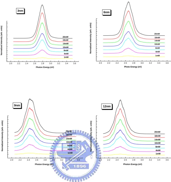
The CW PL spectra of these four samples measured at room temperature are shown in Fig. 4.2.1(a). The detailed MQW PL peak emission energy shown in Fig. 4.2.1(b) increases from 2.47eV to 2.79 eV with the decreasing well width could be fully attributed to the quantum size confinement effect. The similar peak energy of the samples of 9 and 12 nm is due to the weak quantum confinement effect in a larger well width. Figure 4.2.1(c) shows the PL peak emission intensity that gradually decreased with the increase of InGaN well width. When the well width is thicker than 6 nm, the PL intensity drops more quickly.The well width of optimal integrated PL intensity for a-plane would be thicker than relative thin polar quantum well [27]. In additional, the material quality, interface roughness and the excitonic Bohr radius would be considered in terms of the determination of optimal well width [7].
4.2.2 Power dependent photoluminescence
We then analyze different power dependences I ~Pα for the samples of different
well widths over a wide range of excitation power where I is the PL intensity, P is the pumping power intensity, and α is the power index. Power dependent PL
measurement was carried out by using the CW 325 nm He–Cd laser which power density was controlled from 2 to 200 mW/cm2.
In Fig.4.2.2, we show that the PL spectrum as a function of the excitation power for the samples with different well width. We obtained unshifted PL peaks with the increasing pumping power density, which is well known for a-plane hexagonal MQWs with the nonpolar characteristic and the flat band structure. [3] The stable spectral peak position under a wide range of excitation powers clearly indicates that the a-plane InGaN/GaN MQWs on the r-plane sapphire are nonpolar and thus free from the built-in electrostatic fields.
Fig.4.2.3 shows the PL integrated intensity among different excitation power density. Generally, I ~ P relation would satisfy with the condition when nonradiative channels saturate and radiative recombination predominates at elevated excitation. The power indices around 1 for our all samples indicate that the radiative recombination dominate in the optical transition [28] and is absolutely independent of InGaN well width, which also give the other evidence that no built-in electric field was observed within our a-plane InGaN/GaN MQWs with different well widths. However, such the a-plane MQWs without the built-in electric field within should not exhibit strong PL intensity dependence on the well width. [29] Other determining factors should account for the PL intensity drop with a thicker quantum well.
4.3 The localization effect of a-plane InGaN/GaN multiple quantum wells
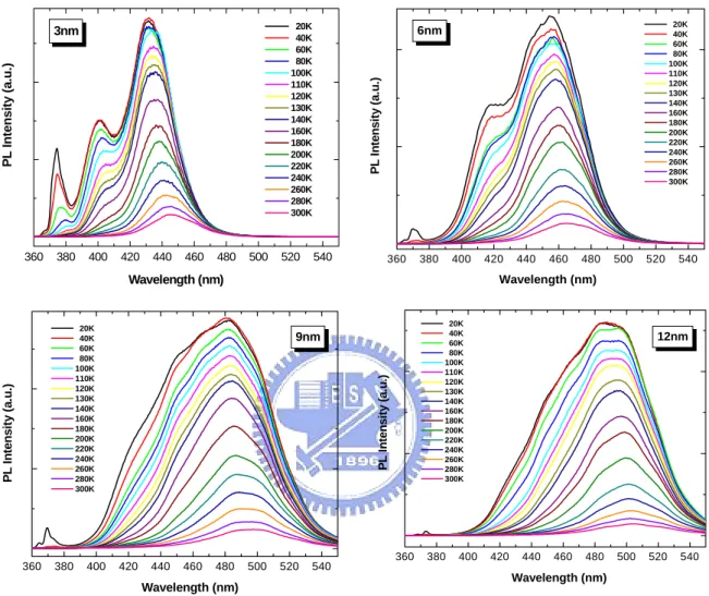
4.3.1 Temperature dependent photoluminescence
In order to further understand whether the localization effect plays an important role in nonpolar InGaN MQWs as well as in polar c-plane InGaN nanostructure or not, PL spectra were measured under different temperature in the range of 20K to 300K using the CW 325 nm He–Cd laser.
Figure 4.3.1 shows the evolution of PL spectra as a function of temperature for the a-plane InGaN/GaN MQWs with well width from 3nm to 12 nm. In these four samples, the decrease of PL intensity with increasing temperature is observed independent of quantum well width. Thermal quenching PL intensity with increasing temperature is a general phenomenon in III-V semiconductor nanostructure which is caused by carriers thermalization from the radiative recombination centers or/and localized states to the nonradiative recombination centers or/and delocalized states. [30] This thermal quenching behavior will be discussed later.
Moreover, at low temperature, there reveals three separated peaks in the PL spectrum, the most high energy peak located around 3.35eV in all samples is suggested to the signal of bulk GaN. The middle energy peak which is obvious in the samples of 3nm and 6nm well width but is merged with the lowest-energy side signal in the samples of 9nm and 12nm well width is supposed to the signal coming
from shallow localized states. [31] The lowest energy signal comes from the deep localized states. As can be seen, only the PL emission from excitons in deep localized states dominates the luminescence from 20K to room temperature, the other two higher energy emissions suffer an apparent quickly thermal quenching when the temperature increases. Along with the increase in temperature, the nonradiative energy relaxation of excitons occurs at shallow localized states, and then the efficient radiative recombination of excitons occurs mainly at deep localized states. The exciton dynamics at shallow delocalized states is very sensitive to the lattice temperature. When the temperature goes up, it is hard for excitons to stay stable in shallow localized states, the thermal dissociation of excitons occurs at shallow localized states, and electrons and holes are thermally excited into the delocalized states, thus, more transfer and relaxation processes happen which quench the emission from high energy states. [31]
Figure 4.3.2 shows the Arrhenius plot of the normalized integrated PL intensity for the a-plane InGaN MQWs emission from deep localized states over the temperature range under investigation. The intensity reduction is remarkable, further compare these four figures, the degree of PL intensity reduction from 20K to 300K is more severe when the well width gets thicker which indicates a higher PL efficiency in the thinner well width samples. [32] We use the equation below to get a good fit to
our experimental data of the activation energy in thermally activated processes [33]:
I(T) = I0/[1+a*exp(-Ea/KBT)+b*exp(-Eb/KBT)] Eq.(4.31.)
where I(T) is the temperature dependent integrated PL intensity, I0 is the integrated
PL intensity at 20K, KB is the Boltzmann’s constant, a and b are the rate constants,
and Ea and Eb are activation energy for two different non-radiative channels. This
suggests that there are two non-radiative paths exist at the same time which one of them dominates in the low temperature region and the other dominate in the high temperature region. [34] The fitting result is listed in table 4.3.1.
Since the activation energy we get from the four samples is much less than the bandgap energy difference between the well and the barrier, it is impossible to account the thermal quenching of InGaN MQWs emission for carriers thermalized from the InGaN wells to the GaN barriers. Therefore, the more reasonable explanation for the quenching of luminescence is that increasing temperature increases the probability of excitons to be trapped by nonradiative recombination centers within the well at the same time when carriers are activated out of the loacalization minima of potential fluctuation which may be caused by compositional、interface fluctuation and indium phase separation that always happened in InGaN quantum well layers.[32]
samples, we further analyze the peak shift of InGaN MQW emission over the investigation temperature range .The result is shown in figure 4.3.3. In the samples with 3nm and 6nm well width, the emission energy decreases monotonically with increasing temperature. However, in the samples with 9nm and 12nm well width, the emission energy decreases at temperatures below 70K with uprising trend, then increases with increasing temperature from 70K to around 140K and finally decreases with further increase of temperature up to the room temperature. This red-blue-red shift of peak energy with increasing temperature is a characteristic of the exciton localization effect. [32, 35] From 20K to 70 K, it is considered that the observed dynamical redshift of the PL spectrum is caused by radiative excitons migrating into lower localized states. At elevated temperature from 70K to 140K, nonradiative recombination processes become more pronounced, some carriers recombination before reaching deeper band-tail states, resulting in a blueshift in the PL peak position. At higher temperature up to 300K, another redshift occurs mainly due to the temperature-dependent dilation of the lattice and electron–lattice interaction. [36-37] Inhomogeneity due to interface fluctuation, InN/GaN segregation, and the band tail states originating from the high density of defects are responsible for the so-called S-shaped temperature dependent behavior in the samples with thicker well width. [33, 38]
Although the emission peak energy of samples with 3 and 6nm well width do not show temperature induced S-curve, it is reasonable to infer that there may be still an exciton localization effect exists to a little extent for the two thinner samples. The total redshifts of the four samples over the temperature range under investigation are: 3nm with 100meV、6nm with 75meV、9nm with 55meV and 12nm with 62meV which indicates that the exciton localization effect may be much stronger in thicker well width. There is one point needed to be noted as compared with the well known shift of the band edge for nitrides of about 65meV without the exciton localization effect in polar structure, the total redshift of the emission peak energy in these four samples from 20K to 300K under the existing of localization effect showed rather big redshift variation with temperature. We couldn't give a clear explanation for such result now, a full understanding of the carrier dynamics in these nonpolar samples will probably emerge only after considerable further study. We can give two key points in this section : the first one is that in a-plane InGaN/GaN MQWs, samples with thicker well width of 9nm and 12nm reveals a more apparent localization effect which is most likely due to alloy、interface roughness fluctuations or worse crystalline quality in the MQWs. The second is that a deeper localization depth may exist in thinner 3nm and 6nm well width samples which could confine carrier tightly thus display an indistinctively visible S-shaped temperature dependent behavior. [39]
4.3.2 Photoluminescence excitation
Photoluminescence excitation (PLE) spectroscopy is a powerful tool for understanding the distribution of energy state and the degree of carrier localization. We proceeded with PL and PLE experiment with the dispersed excitation light comes from the monochrometer in front of a Xe lamp to compare the luminescence and absorption spectra of InGaN MQWs. In PL experiment, the dispersed excitation light wavelength of Xe lamp was fixed at 325nm. While in the PLE experiment, a suitable continuous dispersed excitation light wavelength of Xe lamp was set. In order to get an unambiguous spectrum, both the PL and PLE experiments are carried out at 20K. The experiment result was shown in Fig.4.3.4.
As can be seen, the 20K PL spectra here are the same as those presented in temperature dependent experiment, the lowest energy peak signal in all samples is the emission from deep localized excitons of InGaN MQWs that we really concern about. The detected photon energy of the PLE spectra was tuned at the PL peak position of the four samples. We see that all samples show an absorption feature at energy of about 3.5 eV and a lower tail which is a little bit different dependent on well width. The absorption edge at 3.5 eV is due to carriers being excited in the GaN barriers which then relax into the quantum wells and cause an increase in emission intensity. The undulations in the low energy tails make it difficult to obtain a very precise
estimate of the onset of absorption. Our best estimates for the Stokes shifts of the four samples are 3nm with 140meV, 6nm with 230meV, 9nm with 396meV, and 12nm with 407 meV. We attribute such shift to inhomogeneous broadening localization effect which is expected due to samples' structure and composition non-uniformity. [40-43] A larger Stokes shift and a broaden PLE spectrum are observed when the well width gets wider. A sharp onset of the absorption tail for the 3nm sample indicates a good crystalline quality while a broader PLE spectrum and the appearance of additional weak absorption peaks imply a larger degree of carrier localization in the well regions with wider well width.
4.4 In-plane polarization effect of a-plane InGaN/GaN multiple quantum wells
emission
It was mentioned in section 2.4 that due to the inherent lower symmetry of non-polar heterostructure, a-plane InGaN/GaN MQWs is likely to experience anisotropic in-plane strain. A u-PL measurement was carried out at room temperature using the CW 325nm He-Cd laser and a visible polarizer was set in front of the light collection fiber to examine the polarization property of the four samples. In the case of the a-plane sample, an angle of 900 is defined to be parallel to the c [0001] axis
(E║C) while the 00 is along m [1100] axis (E⊥C). The definition of crystal axes is − shown in figure 4.4.1.
Figure 4.4.2 displays the polarization–dependent PL spectra of 3nm well width sample for polarization angles between 00 and 3600 in steps of 150. All results of
polarization-dependent experiments were similar in these four samples. The value of polarization degree ρ is defined as
ρ= (I⊥—I║)/ (I⊥+I║) Eq. (4.4.1)
, where I⊥ andI║ are PL intensities for E⊥C and E║C. Figure 4.4.3 shows the pretty
symmetric of the normalized PL intensity versus the in-plane polarization angle. The polarization degree ρ of the four samples are 65.4%、66.8%、56.2%、and 58.3% for 3nm、6nm、9nm、and 12nm well width samples, respectively. No obvious difference
on polarization degree is observed with different well width. Figure 4.4.4 shows the PL spectra of the a-plane InGaN MQWs when the polarization of the emission is perpendicular and papallel to the c axis. According to the definition of crystal axes, the transition lowest in energy is allowed for E⊥C, and the transition under E║C must occur at the higher energy. There is an apparent 40~50meV blueshift of the E║C PL maximum with respect to the E⊥C one in 3nm and 6nm samples, but in the samples of 9nm and 12nm, no observable peak shift is found. We conclude the reason of this phenomenon to a large spectral broadening [44] resulted from a more apparent localization effect due to alloy、interface roughness fluctuations or worse crystalline quality in the thicker MQWs.
4.5 Conclusion
In conclusion, ten pairs of a-plane InGaN/GaN MQWs of well width ranging from 3 to 12 nm grown by MOCVD on r-plane sapphire were investigated. No built-in electric field was observed in the power dependent PL measurement for all samples. However, the PL emission intensity decreases as the quantum well width increased. Moreover, the localization effect of a-plane MQWs was investigated by temperature dependent PL and PLE experiment. The former experiment reveals that a more apparent localization effect existed in a thicker well width which is most likely due to alloy、interface roughness fluctuations or worse crystalline quality in the MQWs. From the PLE experiment, a larger Stokes shift and a broaden PLE spectrum are observed when the well width gets wider. Finally, in-plane polarization effect of a-plane InGaN/GaN multiple quantum wells emission was investigated. An average degree of linear polarization about 60% is got in these four a-plane InGaN/GaN MQWs.
Fig. 4.2.1 (a) Room temperature PL spectra of a-plane InGaN/GaN MQWs with well width ranging from 3 to 12 nm.
Fig. 4.2.1(b)(c) Normalized PL energy peak and intensity plotted as a function of quantum well width.
2.0 2.2 2.4 2.6 2.8 3.0 3.2 3.4 3.6 P L In te ns ity (arb. u n its )
Photon Energy (eV)
3nm 6nm 9nm 12nm 2 4 6 8 10 12 0.2 0.4 0.6 0.8 1.0 N o rm al iz e d PL I n te nsi ty ( a rb. uni ts) Well Width (nm) 2 4 6 8 10 12 2.45 2.50 2.55 2.60 2.65 2.70 2.75 2.80 Em issi o n Peak En er gy ( e V) Well width (nm)
Fig. 4.2.2 PL spectrum as a function of the excitation power for a-plane InGaN/GaN MQWs with different well width.
2.0 2.2 2.4 2.6 2.8 3.0 3.2 3.4 3.6 3nm N o rm a lize d Int e ns ity (a rb . u n its )
Photon Energy (eV) 20mW 18mW 14mW 10mW 8mW 4mW 1mW 2.0 2.2 2.4 2.6 2.8 3.0 3.2 3.4 3.6 6nm 20mW 18mW 14mW 10mW 8mW 4mW 1mW N o rm a liz e d In te n s ity (a rb . u n its )
Photo Energy (eV)
2.0 2.2 2.4 2.6 2.8 3.0 3.2 3.4 3.6 9nm N o rm a liz e d I n te n s ity (a rb . u n it s )
Photon Energy (eV)
20mW 18mW 14mW 10mW 8mW 4mW 1mW 2.0 2.2 2.4 2.6 2.8 3.0 3.2 3.4 3.6 12nm N o rm a liz e d In te n s ity (a rb . u n its )
Photon Energy (eV)
20mW 18mW 14mW 10mW 8mW 4mW 1mW
Fig. 4.2.3 The relation between PL intensity and excitation power density for a-plane InGaN/GaN MQWs with different well width.
1 10 100 0.01 0.1 1 3nm I~P1.05 P L In te n s ity (a rb . u n it s)
Excitation Power Density (W/cm2)
1 10 100 0.01 0.1 1 I~P1.06 6nm P L I n te n s it y (a rb . u n it s )
Excitation Power Density (W/cm2)
1 10 100 0.01 0.1 1 P L Inte ns it y (arb. u nits)
Excitation Power Density (W/cm2) 9nm I~P1.04 1 10 100 0.01 0.1 1 I~P0.99 12nm P L Int e nsit y ( a rb. unit s )
Fig. 4.3.1 PL spectra as a function of temperature from 20K to 300K for a-plane InGaN/GaN MQWs with different well width.
360 380 400 420 440 460 480 500 520 540 Wavelength (nm) 20K 40K 60K 80K 100K 110K 120K 130K 140K 160K 180K 200K 220K 240K 260K 280K 300K 3nm P L Int e nsity ( a .u. ) 360 380 400 420 440 460 480 500 520 540 P L I n te n s ity (a .u .) Wavelength (nm) 6nm 20K 40K 60K 80K 100K 110K 120K 130K 140K 160K 180K 200K 220K 240K 260K 280K 300K 360 380 400 420 440 460 480 500 520 540 P L In te n s ity ( a .u .) 20K 40K 60K 80K 100K 110K 120K 130K 140K 160K 180K 200K 220K 240K 260K 280K 300K 12nm Wavelength (nm) 360 380 400 420 440 460 480 500 520 540 20K 40K 60K 80K 100K 110K 120K 130K 140K 160K 180K 200K 220K 240K 260K 280K 300K P L In te n s ity (a .u .) Wavelength (nm) 9nm
Fig. 4.3.2 Normalized integrated PL intensity as a function of 1/T for the a-plane InGaN/GaN MQWs with different well width.
0.00 0.01 0.02 0.03 0.04 0.05 0.01 0.1 1 3nm In te g ra te d P L In te n s it y (a .u .) 1/T (1/K) 0.00 0.01 0.02 0.03 0.04 0.05 0.01 0.1 1 6nm In te g ra te d P L In te n s ity (a .u .) 1/T (1/K) 0.00 0.01 0.02 0.03 0.04 0.05 0.01 0.1 1 1/T (1/K) In te g ra te d P L In te n s ity (a .u .) 9nm 0.00 0.01 0.02 0.03 0.04 0.05 0.01 0.1 1 1/T (1/K) In te g ra te d P L In te n s ity (a .u .) 12nm
3nm 6nm 9nm 12nm
E1(meV) 46.5 9.7 22.4 33.4
E2(meV) 166.5 86.7 106.4 144.9
Table 4.3.1 The fitting result of activation energy for the a-plane InGaN/GaN MQWs with different well width.
Fig. 4.3.3 PL peak energy position as a function of temperature for a-plane InGaN/GaN MQWs with different well width.
0 50 100 150 200 250 300 2.76 2.77 2.78 2.79 2.80 2.81 2.82 2.83 2.84 2.85 2.86 2.87 2.88 3nm Peak En erg y ( eV) Temperature (K) 0 50 100 150 200 250 300 2.64 2.65 2.66 2.67 2.68 2.69 2.70 2.71 2.72 2.73 2.74 2.75 6nm Peak Ener g y ( eV ) Temperature (K) 0 50 100 150 200 250 300 2.47 2.48 2.49 2.50 2.51 2.52 2.53 2.54 2.55 2.56 2.57 9nm Peak En erg y ( eV ) Temperature (K) 0 60 120 180 240 300 2.43 2.44 2.45 2.46 2.47 2.48 2.49 2.50 2.51 2.52 2.53 12nm P eak E n er g y ( e V) Temperature (K)
Fig. 4.3.4 PL and PLE spectra of a-plane nonpolar InGaN/GaN MQWs samples with different well width.
1 . 8 2 . 0 2 . 2 2 . 4 2 . 6 2 . 8 3 . 0 3 . 2 3 . 4 3 . 6 In te n s ity (a.u .) E n e r g y ( e V ) 2.86eV 2.74eV 2.56eV PL PLE 3nm 6nm 9nm 12nm 2 200KK SS=140meV SS=230meV SS=396meV SS=407meV 2.51eV
Fig. 4.4.1 The wurtzite GaN unit cell and the definition of crystal axes.
Fig. 4.4.2 μ-PL spectra of the a-plane InGaN/GaN MOWs for polarization angles between 00 and 3600 in steps of 150.
y (0
0,m-plane)
x (a-plane)
z (90
0,c-plane)
350 400 450 500 550 600 3nm In te n s ity (a rb . u n its ) Wavelength (nm) 00 150 300 450 600 750 900 1050 1200 1350 1500 1650 1800 1950 2100 2250 2400 2550 2700 2850 3000 3150 3300 3450 3600Fig. 4.4.3 Normalized μ-PL intensity versus the in-plane polarization angle for the a-plane InGaN/GaN MOWs with different well width.
0.2 0.4 0.6 0.8 1.0 0 30 60 90 120 150 180 210 240 270 300 330 0.2 0.4 0.6 0.8 1.0 3nm 0.2 0.4 0.6 0.8 1.0 0 30 60 90 120 150 180 210 240 270 300 330 0.2 0.4 0.6 0.8 1.0 6nm 0.2 0.4 0.6 0.8 1.0 0 30 60 90 120 150 180 210 240 270 300 330 0.2 0.4 0.6 0.8 1.0 9nm 0.2 0.4 0.6 0.8 1.0 0 30 60 90 120 150 180 210 240 270 300 330 0.2 0.4 0.6 0.8 1.0 12nm
Fig. 4.4.4 Normalized μ-PL spectra for E//c (900) and E⊥c (00) for the a-plane
a-plane InGaN/GaN MOWs with different well width.
2.50 2.55 2.60 2.65 2.70 2.75 2.80 2.85 2.90 0.2 0.4 0.6 0.8 1.0 1.2 00 900 6nm N o rm a liz e d P L In te n s it y ( a rb . u n its )
Photon Energy (ev)
2.69eV 2.74eV 2.60 2.65 2.70 2.75 2.80 2.85 2.90 2.95 3.00 0.2 0.4 0.6 0.8 1.0 1.2 00 900 3nm N o rm a liz e d P L In te n s ity ( a rb . u n its )
Photon Energy (eV)
2.81eV 2.85eV 2.35 2.40 2.45 2.50 2.55 2.60 2.65 2.70 2.75 0.2 0.4 0.6 0.8 1.0 1.2 00 900 9nm N o rm a liz e d P L In te n s ity (a rb . u n it s )
Photon Energy (ev)
2.35 2.40 2.45 2.50 2.55 2.60 2.65 2.70 2.75 0.2 0.4 0.6 0.8 1.0 1.2 00 900 12nm N o rm a liz e d P L In te n s ity (a rb . u n its )
Chapter 5 Optical properties of a-plane InGaN/GaN MQWs (II)
5.1 Introduction
Time-resolved photoluminescence (TRPL) is an indispensable technique to study the recombination mechanisms of carriers based on radiative, nonradiative, and localization processes. Among the main factors influencing the device performance is luminescence lifetime. In order to further understand the mechanisms of carrier or/and excitons transition process in a-plane InGaN MQWs, we carried out three types of TRPL experiments to clarify the circumstances.
In section 5.2.1, low temperature TRPL was first performed at low temperature 9K to examine the initiative exciton lifetime relative to different quantum well width. In section 5.2.2, PL and the PL decay time as a function of monitored photon energy at 9K were presented, the fittings of experiment data give more evidences to character the localization effect in these samples. Temperature-dependent TRPL was performed in section 5.2.3 which displayed the competition between radiative recombination and nonradiative recombination with increasing temperature, different emission efficiency of the four samples was also revealed in this experiment.
All low temperature and temperature dependent time-resolved PL measurements were performed using time-correlated single-photon counting and a pulsed GaN diode laser operating at a wavelength of 396 nm as the excitation source. The pumped
effective carrier density was estimated to be about 1.27╳1010 cm−2, which was in the
low excitation condition to prevent the strong carrier-carrier scattering. The instrument response of this time-correlated single-photon counting system is about 300 ps.
5.2 Time-resolved photoluminescence
5.2.1 Low temperature TRPL
Figure 5.2.1(a) shows the low temperature time-resolved PL decay for samples with different well widths. Since the measurement was carried out at 9 K, the influence of the nonradiative recombination process could be excluded. [13] All experiment data were fitted by an exponential and a stretched exponential line shape
I(t) = I1(0)exp(−t /τ1)+I2(0)exp[− (t /τ2)β] Eq. (5.2.1) which has been used to analyze the emission characteristics of nonpolar InGaN/GaN MQWs. [4,13] The parameter I(t) means the PL intensity at time t, β is the dimensionality of the localizing centers, and τ1 and τ2 are the initial lifetimes of
carriers. The fast decay timeτ1 (τ1=0.57–1.41 ns) represents the radiative
recombination of free excitons and the relaxation of QW excitons from free or extended states toward localized states. The slow decay timeτ2 (τ2=3.06–22.49 ns)
![HPSH [ 分子間作用力 - 凡得瓦力 ]](data:image/gif;base64,R0lGODlhAQABAIAAAP///wAAACH5BAEAAAAALAAAAAABAAEAAAICRAEAOw==)