多媒體系統晶片平台的設計與應用
113
0
0
全文
(2) 多媒體系統晶片平台設計與應用 Design and Application of Multimedia System-on-Chip Platform 研 究 生:鍾仁峯. Student:Jen-Feng Chung. 指導教授:林進燈. Advisor:Chin-Teng Lin. 國 立 交 通 大 學 電 機 與 控 制 工 程 學 系 博 士 論 文. A Thesis Submitted to Department of Electrical and Control Engineering College of Electrical and Computer Engineering National Chiao Tung University in Partial Fulfillment of the Requirements for the Degree of Doctor of Philosophy in Electrical and Control Engineering. March 2006. Hsinchu, Taiwan, Republic of China. 中華民國 九十五 年 三 月.
(3) 多媒體系統晶片平台設計與應用 學生:鍾仁峯. 指導教授:林進燈 博士 國立交通大學電機與控制工程學系. 摘. 要. 多媒體訊號處理涵蓋兩大核心領域,一為影像及視訊處理,另一為語音及音效 處理。它的應用適合於家庭娛樂系統中及資訊科技產業,具體的產品包括寬頻網路 影音系統、數位廣播系統、多聲道視聽系統、及高音質隨身音樂媒體等。這些系統 為了滿足人類聽覺的需要,即時運算是必須的。然而,多媒體處理計算的需求是由 訊號處理的工作分配,若執行高的取樣頻率也就是處理較大的資料量,則需要複雜 運算。以多媒體的角度而言,它必須處理多不同類型的數據,但使得處理的工作變 得複雜化。本論文針對特別利用在語音與音訊處理上的計算特性,開發出一種新型 的多媒體處理的架構來解決快速驗證平台的問題。 多媒體系統晶片平台的開發以聲音為導向,針對消費性 3C 產品做整合性的開 發設計,它不僅適用多聲道音源輸入與不同喇叭或耳機輸出都可以增強音效的 SoC 雛型設計環境,以便對所需求的規格來確定主系統的架構。在這個規劃中我們提出 了三階段的週期:系統規劃週期、系統設計週期、及系統驗證週期。多媒體系統處理 核心為模組控制,模組控制就像是一個軟體的智財 (IP) 插座,可以透過相同的電 子設計自動化 (EDA) 平台環境進行整合,以微處理器來分配系統資源,提供數位 訊號處理器執行所需的功能。系統匯流排依循 AMBA 匯流排的時序設計,並提供 IP 標準的的介面,充分發揮系統執行的效能。用傳統微處理器和數位訊號處理器的. i.
(4) 相互搭配架構,是未來數位電子的趨勢,亦是降低硬體成本的考量。 本論文中的多媒體系統晶片平台提出了一個 FPGA 的設計與驗證方法,系統晶 片設計部分包含了系統匯流排、微處理控制器、周邊數位 I/O、16 位元空間迴響器、 及 24 位元適用於音訊系統之數位訊號處理器等。可程式化微處理控制器負責系統 晶片內部的流程處理和周邊 I/O 控制;24 位元數位訊號處理器因其架構與指令集是 特別針對音訊系統的主要演算法做考量;16 位元空間迴響器則是一個即時 3-D 音效 處理的智財 (IP),這兩個處理器分別並連接於高速及周邊匯流排上。系統晶片驗證 部分包含語音線性估測編碼的參數求取、音高位置估測、和空間迴響器等演算法的 資料測試與訊號驗證。此平台搭配處理器指令與 gated-clock 的方法,可適應性的 調整算數邏輯單元的使用,具有省功率運作的特性,非常適合音訊多媒體系統中可 攜式與低功率要求的應用。使用 FPGA 經過驗證與測試整個系統的執行效能平均達 80MIPS,功率消耗在 90mW。此設計是跨平台的實現方法,未來可整合到任意單一 矽晶片之中。. ii.
(5) Design and Application of Multimedia System-on-Chip Platform Student:Jen-Feng Chung. Advisor:Chin-Teng Lin. Department of Electrical and Control Engineering National Chiao Tung University. Abstract Multimedia signal processing involves two important fields: one is image and video processing; the other is speech and audio processing. It is suitable to be applied into the system of home entertainment and the industry of information technology, for example, the concrete products such as a wide-band video-audio system of networks, a digital broadcast system, a multi-channel video-audio system, a high-quality walkman, etc. To satisfy the requirement of human hearing, it is necessary for real-time processing. However, the assignment of multimedia signals depends on the requirement of computational power. If a system has to process mass data, i.e., high operating frequency, it should perform complex operations. Because data is composed of different signals in the multimedia world, the work of signal processing becomes complication. In this thesis, we make use of computational characteristics of speech and audio processing and design a new architecture of multimedia processing in order to solve the problem of verification quickly. Based on the conception of sound processing, a multimedia System-on-Chip (SoC) platform, which can integrate 3C consumer products, is designed. It is not only suitable for multi-channel sound input or output such as speakers or headsets, but also achieves iii.
(6) the effect of virtual sound. We are in accordance with three phase cycles as specification, design, and verification for assisting the platform design. The kernel of the SoC platform is like a module control. The module control is just like as the software socket of intelligence property (IP). Thus, we can integrate with IPs via the environment of electronic design automation (EDA). In the platform, a microprocessor is as the master to assign system resources. The system bus meets the timing of AMBA and offers the standard AMBA interface to promote performance and to reduce hardware costs. The architecture of traditional microprocessor and digital signal processor (DSP) is the trend of digital circuit design in the future. In this thesis, we present design and verification of the multimedia SoC platform. The platform design integrates the system bus, microprocessor, memory controller, peripheral I/O, 16-bit reverberator, 24-bit DSP, etc. The programmable microprocessor manages internal data flow and digital I/Os. The 24-bit DSP is specified as its architecture and instruction set for sound algorithms. The 16-bit reverberator is 3-D virtual sound IP performed in real time. The two processors are connected to the high-performance bus (AHB) and the peripheral bus (APB), respectively. The platform verification includes the speech parameters of linear predictive coding, pitch estimation, and reverberation. These algorithms are used to test data flows and to verify functionality for the proposed SoC platform. By using the gated-clock scheme, the platform has reducing power characteristics so that it can adaptively adjust the usage of parallel ALUs. Finally, under FPGA verification and testing, on average the whole performance obtains 80MIPS, and power consumption is about 90mW. Due to a cross-platform implemented scheme, it can be applies into an embedded and portable multimedia system and can also be integrated to a single silicon chip.. iv.
(7) 誌. 謝. 在交大電機與控制工程系攻讀博士的期間,似乎都在和時間競逐下過日 子,不但修課考試要花時間,想研究內容也要花時間,實驗與寫作更花時間。 不論何時何地,都和時間在競賽,這些都在磨練我的體力與耐力,雖然心力 交瘁,最後還是走完這一段人生重要的過程。 首先要感謝我的指導教授—林進燈教授,因為我遇到一個優秀的,並給 了我彈性與自治,他的精闢見解與專業知識適時地修正我的方向,給予寶貴 的建議,彌補我研究經驗的不足,使我省下不必要的時間浪費;他的治學態 度嚴謹又不失務實,不僅在學業方面的悉心指導,更在爲人處世及求學態度 上給予啟蒙及悉心指導,讓我學習到許多寶貴的知識與經驗,使得本論文能 順利完成。另外也要感謝口試委員們的建議與指教,使得本論文更為完整。 其次,感謝曾提供我相當多協助實驗室的學長:勝富、得正、鶴章,與 學弟妹們建志、龍吉、亙志、長茂、朝暉、世安、育緯、晴慧、家昇、經翔、 峻谷、紹航等,以及我身邊的好朋友們,在研究過程中所給我的鼓勵、協助 與支持;其實該感謝的人很多,無法一一道盡,只有將感激收藏在心裡。 最後,更要感謝我的父母親對我的教育與栽培,給予我一切鼓勵與協助, 使我能安心無負擔的完成博士學業。僅將本論文獻給我的家人所有關心我的 師長與朋友們,願他們共享這份榮耀。. 仁峯 於交通大學電控系資訊媒體實驗室 2006.3.15. v.
(8) TABLE OF CONTENTS 摘. 要 ................................................................................................................................... I. ABSTRACT............................................................................................................................... III 誌. 謝 ..................................................................................................................................V. TABLE OF CONTENTS.......................................................................................................... VI LIST OF TABLES .................................................................................................................... IX LIST OF FIGURES ....................................................................................................................X LIST OF FIGURES ....................................................................................................................X CHAPTER 1 INTRODUCTION TO MULTIMEDIA PROCESSING...................................1 1.1 INTRODUCTION .........................................................................................................1 1.2 MOTIVATION...............................................................................................................2 1.3 OBJECTIVES................................................................................................................4 1.4 ORGANIZATION OF THE THESIS ............................................................................8 CHAPTER 2 MULTIMEDIA IN SOUND PROCESSING......................................................9 2.1 INTRODUCTION .........................................................................................................9 2.2 ARTIFICIAL REVERBERATION................................................................................9 2.2.1 FILTERS................................................................................................................11 2.2.2 FIR EARLY REFLECTION ..................................................................................12 2.2.3 REVERBERATOR ................................................................................................13 2.3 SPEECH PROCESSING .............................................................................................17 2.3.1 LINEAR PREDICTIVE CODING........................................................................17 vi.
(9) 2.3.2 PITCH ESTIMATION ..........................................................................................19 CHAPTER 3 DESIGN OF APPLICATION-DRIVEN DIGITAL SIGNAL PROCESSOR ..........................................................................................................................21 3.1 INTRODUCTION .......................................................................................................21 3.2 MICRO-ARCHITECTURE.........................................................................................22 3.3 INSTRUCTION SET...................................................................................................27 3.3 ADDRESSING MODES .............................................................................................28 3.4 MATRIX PROCESSING TECHNIQUE ....................................................................30 3.5 VECTOR PROCESSING TECHNIQUE ....................................................................32 3.6 DMA AND INTERRUPT INTERFACE .....................................................................34 3.7 POWER OPTIMIZATION ..........................................................................................37 3.8 COPROCESSOR: REVERBERATOR........................................................................39 3.9 DEVELOPMENT SOFTWARE ..................................................................................43 CHAPTER 4 SIMULATION RESULTS .................................................................................48 4.1 SPEECH PROCESSING .............................................................................................48 4.1.1 LPC AND PITCH ESTIMATION .........................................................................48 4.1.2 MELP CODING ....................................................................................................51 4.1.3 POWER ANALYSIS .............................................................................................54 4.2 REVERBERATION ALGORITHM ............................................................................56 4.2.1 DSP PROGRAMMING.........................................................................................56 4.2.2 IMPLEMENTATION OF APPLICATION-SPECIFIC REVERBERATOR .........59. vii.
(10) 4.3 PERFORMANCE ANALYSIS OF LASP24 ...............................................................61 CHAPTER 5 THE INTEGRATED PLATFORM FOR MULTIMEDIA PROCESSING ..63 5.1 INTRODUCTION .......................................................................................................63 5.2 SOC PLATFORM........................................................................................................64 5.3 INTELLECTUAL PROPERTY DESIGN ...................................................................67 5.3.1 MICROPROCESSOR ...........................................................................................67 5.3.2 INTER-IC SOUND INTERFACE.........................................................................69 5.3.3 SERIAL COMMUNICATION DESIGN...............................................................72 5.3.4 WRAPPER AND INTERRUPT DESIGN.............................................................74 5.3.5 SPECIALIZED HARDWARE FOR SYSTEM VERIFICATION.........................76 5.4 SYSTEM PROTOTYPE..............................................................................................78 CHAPTER 6 CONCLUSIONS AND FUTURE WORKS......................................................81 BIBLIOGRAPHY......................................................................................................................85 APPENDIX A LASP24 INSTRUCTION SET AND EXAMPLES........................................92 APPENDIX A LASP24 INSTRUCTION SET AND EXAMPLES........................................92 APPENDIX B ADDRESSING MODES...................................................................................96 VITA............................................................................................................................................97 PUBLICATION LISTS .............................................................................................................98. viii.
(11) LIST OF TABLES. TABLE 3-1. THE MATRIX COORDINATE FOR THE MATRIX ADDRESSING MODE, WHERE AR0L AND AR1L REPRESENT THE LOWER FOUR BITS OF AR0 (AR0[3:0]) AND AR1 (AR1[3:0]), RESPECTIVELY....................................................................................... 31 TABLE 3-2. THE FORMAT OF THE VECTOR ADDRESSING MODE AND THE REPRESENTATION OF VECTOR ADDRESSES IN. LASP24, WHERE OP INDICATES OPERATION; VA, VB, AND. VC REPRESENT VECTOR REGISTERS. THE SYMBOLS, FIL, EXT, WIN, RAM0, AND RAM1, ARE MEMORY SYMBOLS............................................................................... 33 TABLE 4-1. SIMULATION RESULTS OF LPC CALCULATIONS IN DIFFERENT FLOATING-POINT PRECISION................................................................................................................. 49. TABLE 4-2. TIMING SIMULATION RESULTS. THE TIME UNIT OF EXECUTION IS MICROSECOND (MS), AND THE TOTAL TIME OF EXECUTION IS THE SUM OF LPC AND PE COMPUTATION TIME. ................................................................................................ 50. TABLE 4-3. BIT ALLOCATION FOR THE MELP CODER ................................................................. 53 TABLE 4-4. POWER DISSIPATION ANALYSIS OF LASP24. ........................................................... 55 TABLE 4-5. ALLPASS FILTER COEFFICIENTS. ............................................................................... 58 TABLE 4-6. COMB FILTER COEFFICIENTS. ................................................................................... 58 TABLE 4-7. COMPARISON. OF. DIFFERENT. FIR. SCHEMES. FOR. EARLY. REFLECTION. IMPLEMENTATION. .................................................................................................... 60. TABLE 4-8. COMPLEXITY COMPARISON BETWEEN LASP24 AND MEMORY WITH OPTIMIZATION CODES....................................................................................................................... 62. TABLE 5-1. MODULE DESIGN OF THE SOC PLATFORM................................................................ 65 TABLE 5-2. MICROPROCESSOR’S ALTERNATE FUNCTIONS. ........................................................ 69 TABLE 5-3. THE FPGA SYNTHESIS RESULTS OF AUDIO SOC DESIGN. ......................................... 78 ix.
(12) LIST OF FIGURES FIG. 1-1.. COMPONENTS OF A TYPICAL MEDIA PROCESSING SYSTEM. ............................................ 5. FIG. 2-1.. IDEAL IMPULSE RESPONSE OF AN ACOUSTIC ROOM. ..................................................... 10. FIG. 2-2.. (A)ALL-PASS FILTER AND (B) MODIFIED COMB FILTER, WHERE M, G, A REPRESENT THE DELAY LENGTH, THE GAIN FACTOR, AND THE COEFFICIENT, RESPECTIVELY................. 12. FIG. 2-3.. IMPULSE RESPONSE WITH EARLY REFLECTIONS. .......................................................... 12. FIG. 2-4.. IMPULSE RESPONSE WITH EARLY REFLECTIONS. .......................................................... 13. FIG. 2-5.. THE PROPOSED ARCTICTURE OF REVERBERATOR. ........................................................ 14. FIG. 2-6.. (A) FIR MODELING WITH EXPONENTIALLY-DECAYING PSEUDO-RANDOM COEFFICIENTS; (B) ADDITIONAL COLORING PHENOMENON OF A COMB FILTER; AND (C) COLORING REDUCTION. .................................................................................................................. 15. FIG. 2-7.. THE UN-WEIGHTED PSEUDO-RANDOM FIR SEQUENCE OF 1'S, 0'S, AND -1'S WITH 4,000 (LEFT) AND 14,400 (RIGHT) DENSITIES PER SECOND OF NON-ZERO FILTER TAPS, RESPECTIVELY............................................................................................................... 17. FIG. 3-1.. HARDWARE/SOFTWARE DEVELOPMENT FLOW FOR LASP24........................................ 22. FIG. 3-2.. THE BLOCK DIAGRAM OF THE PROPOSED DIGITAL SIGNAL PROCESSOR. ...................... 24. FIG. 3-3.. PIPELINING OPERATIONS............................................................................................... 25. FIG. 3-4.. BRANCH OPERATIONS. .................................................................................................. 26. FIG. 3-5.. MEMORY ACCESSING OPERATIONS. .............................................................................. 27. FIG. 3-6.. ILLUSTRATION FOR COMPUTING A MATRIX ADDRESS WITH THE VECTOR ADDRESSING MODE. ........................................................................................................................... 31. FIG. 3-7.. AN EXAMPLE OF MEMORY OPERATIONS IN LASP24, WHERE OP INDICATES THE VECTOR MULTIPLICATION. VA, VB, AND VC REPRESENT DIFFERENT MEMORY BANKS. THEY ARE DEFINED IN TABLE TABLE 3-2....................................................................................... 32. x.
(13) FIG. 3-8.. GENERATION OF LASP24’S INTERRUPT FOR A SINGLE PERIPHERAL DEVICE VIA INTERRUPT REQUEST FLAG............................................................................................ 36. FIG. 3-9.. THE GATED-CLOCK SCHEME IN (A) PARALLEL ARITHMETIC UNIT, (B) CLOCK GATING, AND (C) POWER SAVING PARALLEL ARCHITECTURE. .................................................... 38. FIG. 3-10. THE PROPOSED PSEUDO-RANDOM FIR ARCHITECTURE WITH TWO-STAGE PIPELINE. THE ADDER IS A. 2’SC ADDITION OPERATION. THE MULTIPLIER LIMITED BY THE NON-ZERO. CONTROL IS A UNIT MULTIPLICATION OPERATION......................................................... 40. FIG. 3-11. THE COMPUTATIONAL DIAGRAM OF THE CIRCULAR BUFFER WHEN THE ADDRESSING INDEX INDICATES (A) J=0, (B) J=510, AND (C) J=2000. ................................................. 42. FIG. 3-12. FULLY FSM CONTROL FLOWS FOR TWO-STAGE ARCHITECTURE. ................................. 42 FIG. 3-13. THE STRUCTURE OF DEFY-I FOR LASP24. .................................................................. 43 FIG. 3-14. OPERATION OWS OF THE EMULATOR............................................................................. 44 FIG. 3-15. THE HARDWARE EMULATOR. ........................................................................................ 45 FIG. 4-1.. THE MICROPROGRAMMING FLOW IN THE PROGRAM ROM OF LASP24. ...................... 49. FIG. 4-2.. PERFORMANCE COMPARISONS OF LASP24 AND TMS320C3X. ................................... 51. FIG. 4-3.. THE ORIGINAL AND RESULTING WAVEFORMS AFTER THE REVERBERATION ALGORITHM: (A) IS A SIMULATED IMPULSE RESPONSE WITH EARLY REFLECTION IN FIR; (B) IS FIR COEFFICIENTS USING A PSEUDO RANDOM METHOD; (C) AND (E) ARE ORIGINAL AUDIO MUSIC AND FEMALE SPEECH WITH 44.1 KHZ SAMPLING RATE AND 16-BIT DATA FORMAT;. (D) AND (F) ARE THE SIGNALS AFTER PROCESSING (C) AND (E). ................................... 59 FIG. 4-4.. FULLY FSM CONTROL FLOWS FOR TWO-STAGE ARCHITECTURE. ................................. 59. FIG. 4-5.. SOUND WITH 2,0282 DIGITAL SAMPLES AFTER FIR PROCESSING: (A) DESIRE RESULTS AND (B) DESIGN RESULTS. (C) AND (D) ARE THE RESULTS OF FREQUENCY DOMAIN ANALYSIS WITH HAMMING WINDOW FOR (A) AND (B).................................................. 61. FIG. 5-1.. MULTIMEDIA SOC PLATFORM: (A) SOC ARCHITECTURE AND (B) THE PROPOSED PROTOTYPE SYSTEM. .................................................................................................... 67. xi.
(14) FIG. 5-2.. THE BASIC INTERFACE TIMING OF I2S. .......................................................................... 70. FIG. 5-3.. THE BLOCK OF AUDIO I2S CONFIGURATION (SCK=64×FS AND WS=FS=48KHZ)........... 71. FIG. 5-4.. FPGA SIMULATION OF I2S TRANSMISSION.................................................................... 72. FIG. 5-5.. THE BLOCK DIAGRAM OF UART (BAUD RATE AT 9,600 B/S). ....................................... 73. FIG. 5-6.. FPGA SIMULATION OF UART (A) RECEIVER AND (B) TRANSMITTER. .......................... 74. FIG. 5-7.. FPGA SIMULATION OF DATA TRANSFER FOR 8051 WRAPPER........................................ 75. FIG. 5-8.. COMPLETE STAT MACHINE FOR 8051 WRAPPER............................................................ 76. FIG. 5-9.. EMULATION TESTBENCH............................................................................................... 77. FIG. 5-10. SHARE MEMORY: (A) THE DATA FORMAT AND CONTROL OF AUDIO STREAMING AND (B) SIMULATION RESULTS OF PROCESSING THREE-CHANNEL DATA IN THE DUAL-PORT. SRAM........................................................................................................................... 79 FIG. 5-11. (A) THE FINAL DEMO BOARD AND (B) THE INITIAL DEVELOPMENT ENVIRONMENT. .... 80. xii.
(15) CHAPTER 1 INTRODUCTION TO MULTIMEDIA PROCESSING. 1.1 Introduction Multimedia signal processing, which represents a major part of the latter category, involves the joint processing of digital information in various representations. It covers a very broad spectrum of applications: ●. Audio and speech processing: audio compression, Dolby surrounding;. ●. Image and video processing: resolution conversion, image enhancement, image restoration, image and video compression;. ●. Content-based indexing and retrieval: feature extraction, pattern recognition, face detection/recognition, fusion of multi-modality;. ●. 2-D. and. 3-D. graphics:. volume. rendering,. modeling. transformation,. computer-assisted animation, virtual reality, etc. As speech, audio, image, and video are playing increasingly dominant roles in multimedia information processing, content-based retrieval has a broad spectrum of application. Processing the signal using a filter circuit can remove or at least reduce the unwanted part of the signal. Increasingly nowadays, the filtering of signals to improve signal quality or to extract important information is done by digital signal processing techniques rather than by analog electronics.. 1.
(16) 1.2 Motivation Multimedia systems [1] have attracted considerable media attention because of their promise to transform ordinary personal computers into entertainment centers that also function as powerful business tools. However, applications for these systems also present major design challenges to processor developers because multimedia applications such as video games, Dolby AC-3, and MPEG-2 video [2] have a mix of processing requirements that go beyond the capabilities of general-purpose processors. Multimedia applications [8] must not only meet stringent specifications including real-time processing, low-power dissipation, and small die size, but also be inexpensive for access to the consumer market. For the multimedia market, processor developers must have the utmost sensitivity toward the processors effect on the final product’s price. Because of this, the processor must reach a balance where hardware utilization is maximized while at the same time allowing for enough throughputs to be achievable for several applications. A number of standards have been proposed in the field of audio and video compression [3]. Communication applications, such as video telephony, are covered by the ITU-T standards H.261 and H.263 [61]-[62]. Playback of video stored on CD-ROM, TV broadcast, and video-on-demand are applications aimed by the ISO standards MPEG-1 and MPEG-2. Other important multimedia signal processing algorithms beside compression deal with content-based indexing and retrieval, speech analysis and synthesis, 2- and 3-D image animation, or scene modeling and understanding. The growing complexity of the algorithms, often associated with real-time constraints, leads to increasing computational demands. Having to deal with multiple streams of different data types further complicates the processing in a multimedia environment. Multimedia processing requests extreme demands on computing-, transmission-, and. 2.
(17) storage-devices. Especially video consists of large data volumes, which makes it difficult to handle the data in their raw form. Therefore, compression is a key technology for multimedia applications. Thus, it is necessary for a powerful digital signal processor (DSP). Like a general-purpose microprocessor, DSP is a programmable device, with its own native instruction code. DSP is the capable of carrying out millions of floating point operations per second, and like their better-known general-purpose cousins, faster and more powerful versions are continually being introduced. It can also be embedded within complex “system-on-chip” devices, often containing both analog and digital circuitry. To perform multimedia tasks, many companies develop dedicated hardware such as hardwired solutions customized for a given application [2]-[8], or specialized processors that appear to be hardwired solutions [9]-[10]. These designs work well for their intended purposes but their inherent inflexibility forces developers to make modifications for each new application. Furthermore, dedicated hardware means that design engineers must refamiliarize themselves with a new architecture for each new system they develop. While complexity and sophistication of multimedia algorithms continue to grow, commercial success of multimedia applications essentially relies on efficient VLSI implementation [60]. Today’s standard processing devices are generally not able to fulfill the demands of multimedia processing without special adaptation. Programmable high-end general-purpose processors, as designed for the PC and workstation market, are typically weak at signal processing and moreover too expensive and power-consuming for standalone multimedia applications. Conventional digital signal processors, although optimized for processing of speech and audio signals, still lack the required high performance for video signal processing. In consequence, special architectural approaches are required to deliver sufficient multimedia processing performance at low cost. Currently available standard processing devices are not able to fulfill the requirements 3.
(18) of multimedia processing without special adaptation. Architectural enhancements have therefore been introduced aiming to exploit the special algorithm characteristics. Current processors, however, mainly rely on massively available data parallelism and highly predictable program flow to achieve performance gains. While this approach is feasible for algorithms dominated by block-based processing style, as encountered, e.g., in traditional video compression schemes, it will not be sufficient for emerging applications characterized by higher complexity and decreasing computational predictability. This thesis discusses innovative architectural approaches that promise a more exhaustive exploitation of parallelism and a more flexible utilization of processing resources. First, computational characteristics of current and future multimedia algorithms are analyzed. Then, architectural enhancements employed - by state-of-the-art multimedia processors with multi-core architecture [75], mainly targeting compression schemes, are shortly reviewed. The remaining part of the thesis presents reconfigurable computing, simultaneous multi-threading, and associative controlling as three promising architectural concepts able to deal with the future demands of emerging multimedia applications.. 1.3 Objectives Consider the components of a typical media processing system, shown in Fig. 1-1. Here, an input source presents a data stream to a processor’s input interface, where it is manipulated appropriately and sent to a memory subsystem. The processor core(s) then interact with the memory subsystem in order to process the data, generating intermediate data buffers in the process. Ultimately, the final data buffer is sent to its destination via an output subsystem.. 4.
(19) Input Source. Input Subsystem. Core Processing. Output Subsystem. Destination. Memory Subsystem. Fig. 1-1. Components of a typical media processing system.. Multimedia processing is that the actual work done by the media processor core. The input data varies widely in its bandwidth requirements. Raw audio might be measured in tens of kilobits/second (kb/s), and raw video could entail tens of megabytes per second (Mbytes/s). Then, it is clear that the media processor needs to handle different input formats in different ways The computational requirements of multimedia processing are dominated in the first place by the signal processing tasks, requiring complex operations to be performed on large data volumes at high sample rates. Typically, real-time constraints arise from the need to satisfy human sound perception demands. Having to deal with multiple streams of different data types further complicates the processing task. State-of-the-art multimedia architectures employ a number of architectural measures in order to exploit the computational characteristics of speech and audio processing algorithms in particular. So far, the design focus has been on efficient implementation of the computation-intensive low-level parts of the algorithms-as dominating in frame-based schemes. Depending on the targeted application field, dedicated and programmable approaches can be distinguished. The design of dedicated VLSI implementations for selected multimedia processing schemes is driven by the need for inexpensive, highly integrated systems targeting the consumer market. This goal is achieved by deep adaptation of modules to special 5.
(20) algorithms and algorithm classes. Programmable architectures, on the other hand, provide a more general platform, offering the flexibility to allow various algorithms being executed on the same hardware by only software modifications. To achieve computing performance, the application-driven necessity to provide processors with both microprocessor and DSP functionality enforces new architectures and approaches. Simply using two cores—a microprocessor and a DSP core—is multitasking-effective as resources are often doubled. The 24-bit architecture presented here provides general purpose micro-processing as well as DSP functionality through a single-core and a unified architecture, respectively. The optimal solution is an application-oriented processor core [69], [70], having a lower cost than a general-purpose DSP. The parallel architecture of DSP can efficiently execute vector and matrix operations without extra overhead. In order to implement an application-driven DSP, we use a methodology for hardware/software (HW/SW) co-verification [71] and optimize the processor architecture and instruction sets. High flexibility in use, small area on silicon, high data throughput, and fast portability to a wide range of technologies are our main targets in the core development. The modern embedded system has moved toward the target of system integration and implementation. Reuse [50] is done at the chip level called intellectual property (IP) core which represents the functions of specification domains like multimedia applications. These modules are integrated into System-on-Chip (SoC) [72] which is a typical architecture. We investigate architectural techniques to facilitate analysis and integration for heterogeneous and general/complex SoC applications in this thesis. We use a microcontroller and digital signal processor application to validate the embedded platform prototype. The concept of platform refers to a family of architectures satisfying ARM defined constraints [54], and allowing customizations and substantial re-use of hardware. 6.
(21) and software modules. We developed a base architecture with customization or parameterization options to speed-up derivative implementations while reducing the HW/SW overhead. The definition of the SoC platform IP is the result of a trade-off process involving reusability, overall SoC integration effort [67], performance [68] and power optimizations [77]. Our focus is on efficiency of the hardware and software resources in the context of a self-adapting architecture with autonomic features. The motivation for developing such IP is to facilitate integration of SoCs. Because the platform is meant to be easily customized, it is essential to meet stated resource-efficiency goals. The SoC integrated platform provides multi-function system backbone for various multimedia applications. The new proposed SoC integrated platform which combines microprocessor, digital signal processor (DSP), memory, and other functional modules such as GPIO (General-Purpose Input/Output), I2S (Inter-IC Sound), and communication (UART) into a single IC is popular recently. To verify these functions of the proposed platform for audio and speech processing, the FPGA (Field Programmable Gate Array) rapid prototype approach will be used. FPGA were primarily used for prototyping and lower volume applications in years and custom ASICs were used for high volume, cost-sensitive designs. In the thesis, we will describe the proposed platform, IP reuse design experiment based on a methodology in [66]. The contribution of this thesis is to propose a multimedia SoC platform, which can integrate 3C consumer products, for sound processing. The platform can solve low-cost consideration and construct quickly the components of multimedia signal processing in the standard bus. The platform using two cores, a microprocessor and a DSP core, can promote computational performance. Especially DSP, it is designed as the sound signal processor for the consideration of architecture and instruction set, and has low-power characteristics with gated-clock technology [37]. Due to their high capacitive load which makes them a 7.
(22) major contributing factor to the overall power consumption of the SoC device, we take advantage of instruction or control types to decide which component needs to be disabled. In addition, bus encoding techniques [77] can reduce the power consumption on a bus by mapping the information conveyed on the bus to a form which has less transition activity than the original. This is to reduce the consumption of the electric current. Due to cross-platform design which is not limited by any synthesis tool or FPGA, this method can be easily verified and fabricated as ASIC.. 1.4 Organization of the Thesis In this thesis, the rest of the dissertation is organized as follows. Chapter 2 describes in multimedia the application of sound signal processing including artificial reverberation and speech compression. These three sound processing will be applied to the SoC platform. According to the reverberation principle, we design a real-time reverberator with the pseudo-random coefficient method. Afterward, Chapter 3 would implement an application-driven digital signal processor. We consider for special addressing modes, matrix and vector processing, power optimization, and the architecture of reverberator. Continuously, the experimental results and comparison would be illustrated in Chapter 4. In order to be able to apply into the SoC platform for sound signal processing, Chapter 5 constructs a multimedia integrated platform. The platform is controlled by a built-in microprocessor, and it can capture and play sound through the standard inter-IC sound interface. Hence, the multimedia platform can call a programmable SoC platform. Finally, conclusions and future works are made the last chapter.. 8.
(23) CHAPTER 2 MULTIMEDIA IN SOUND PROCESSING. 2.1 Introduction Sound processing is one of the many applications of digital signal processing. Three-dimensional (3-D) sound is becoming increasingly important in scientific, commercial, and entertainment systems [8] for human life. It can greatly enhance auditory interfaces to computers, improve the sense of presence for virtual reality simulations, and add excitement to computer games. Recent extensions of physical and behavioral studies have revealed that the external ear plays an important role in spatial hearing. Due to the rapid growth in computational power, many new virtual auditory systems could be implemented in real time. In the Section, we introduce two techniques of 3-D sound processing as artificial reverberation and one basic speech processing as linear prediction coding (LPC) and pitch estimation (PE), respectively.. 2.2 Artificial Reverberation Today, a multichannel [9] playback system has been frequently used in cinema or home video. In this thesis, a stereo-channel multiband room effect simulator [81] with friendly control interface is presented. In order to obtain different music quality, we design a new room simulator to be suitable for the multichannel surround sound system [10]. The impulse response for room simulation is the result of the many reflections of a sound that occur in a room. The response consists of direct sound, early reflection, and fused reflection. In 1961, the first room effect algorithm was proposed by Schroeder [11]. 9.
(24) Then Schroeder’s algorithm was extended by Moorer [12] in 1978. The room effect introduces a spatial dimension to a piece of recorded sound, which means that it can be used to model a specific acoustic environment in which to affect a dry unaltered signal. Long reverberation times provide the feeling of a large hall, and short reverberation times (RT) give the impression of smaller rooms. We refer to Moorer’s reverberator using FIR and IIR filters to design artificial reverberation called a reverberator. The impulse response for an acoustic room is depicted in Fig. 2-1. This response includes direct sound, early reflections, and late reverberation. The main contribution of this thesis should be a specification of the requirements made on the reverberation algorithm, which will be preparing for real-time processing and multichannel outputs. The reverberation algorithm is based on an exponentially-decaying pseudo-random FIR filter [13] to represent the early reflections segment, with a feedback delay path to create the dense reverberant field. In addition, an equalizer offers the capability of both compensating for defects and fine tuning the system. With an equalizer, certain frequency ranges can be either increased or cut. We also design a 10-band equalizer as like Winamp2 to control how finely the frequency pattern can be amplified or attenuated and setup several selective modes for selection. Finally, the output of the room simulator can be connected to modified 5.1-channel Dolby surround decoder with [14]. Early Reflections. Late Reflections. time. Fig. 2-1. Ideal impulse response of an acoustic room.. 10.
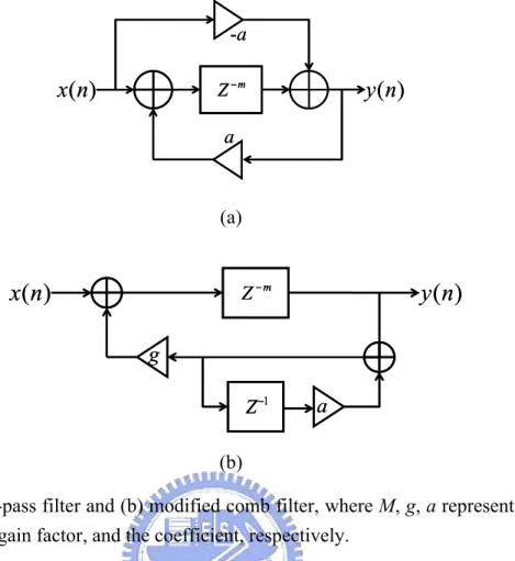
(25) Reverberation [15] is probably one of the most heavily used effects in music. Reverberation effects can be achieved by using any combination of filter techniques. The FIR filter, comb filter, and all-pass filter are the basic structures that have been combined in different ways in an attempt to imitate the effects of various rooms.. 2.2.1 Filters Filtering techniques are used to perform convolution with input sound sources. A FIR filter is used to model the segment of early reflection. This is because each reflected signal could be distinguished by human ears in this segment. The parallel comb filters and cascade all-pass filters are added to generate its late reverberation segment. In order to increase the echo density, the output of the parallel comb filters is fed into one or more all-pass filters (Fig. 2-2(a)) in series. Each all-pass filter has a multiplicative effect on the number of echoes, but prevents coloration due to the all-pass filter’s flat frequency response. In general, a high order FIR filter is considered to model the early reflection segment, but it would take too much execution time for computation. To improve this problem, a simple delayed feedback loop around the FIR early segment is used to reduce the FIR order. The order of the FIR filter is decided by the first comb filter delay and the reverberation length in our system. However, room impulse responses consist of very dense series of echoes that cannot be practically realized using this architecture. Since the eigenfrequencies of rooms have a rapid decay for high frequencies, and a frequency-dependent reverberation time can be implemented with a low-pass filter. Moorer suggested a modified comb filter with a low-pass filter (Fig. 2-2(b)) in feedback loop to take frequency-dependent decay into consideration to solve this problem.. 11.
(26) -a. x (n). y (n). Z −−mm. a. (a). x (n). y (n). Z −−mm. g Z −1. a. (b) Fig. 2-2. (a)All-pass filter and (b) modified comb filter, where M, g, a represent the delay length, the gain factor, and the coefficient, respectively.. 2.2.2 FIR Early Reflection The impulse response of sound consists of direct sound, early reflections shown as Fig. 2 and exponentially decaying late reverberation (with an IIR filter to reduce computational complexity). 0.4 0.3 0.2. Gain. 0.1 0 -0.1 -0.2 -0.3 -0.4 0. 0.05. 1. 1.5. 2. 2.5. 3. Time (sec). Fig. 2-3. Impulse response with early reflections. 12.
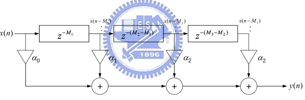
(27) The early reflections often derived from a room model, e.g., as reflections caused by an image source. Reflections during about 20~80ms after sound is triggered are heard together with the direct sound as one single auditory event. An FIR filter is used to generate these early reflections. Since the early reflections are relatively sparse and span a relatively short time, they can be implemented using tapped delay lines (Fig. 2-4). This idea was apparently first suggested by Schroeder in 1970 [11] and evidently first implemented by Moorer [12]. A key parameter in determining the quality of the reverberation is the echo density. In the case, to increase echo density, the FIR order will be large. Of cause, this causes long computing time. Hence, we can increase non-zero values with pseudo-random coefficients and select suitable for memory spaces to reduce the FIR order but not affect sound qualities.. x(n). z − M1. x (n − M 1 ) . .. α0. z − ( M 2 − M1 ). x (n − M 2 ) . .. α1. z −( M 3 −M 2 ). x(n − M 3 ) . .. α2. +. +. α2. +. y (n). Fig. 2-4. Impulse response with early reflections.. 2.2.3 Reverberator Different audio effects can be performed by designing and implementing suitable filters. The proposed reverberator shown in Fig. 2-5 is composed of a FIR filter with pseudo-random coefficients (Fig. 2-6(a)), 10 parallel comb filters, 4 cascade all-pass filters, and a pair of late low-pass filters. The FIR filter models the segment of early reflection. The parallel comb filters and cascaded all-pass filters model the segment of late reverberation, and late low-pass filters are to produce the feeling of the distance from 13.
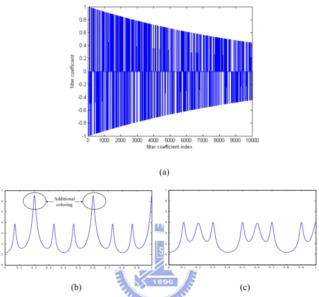
(28) sound source. Note that the delay length of comb filters must be carefully chosen to avoid the coloring phenomenon shown as Fig. 2-6(b) and (c), respectively. The input of the room simulation is the mono signal xR(n) and xL(n) respectively. These two mono input signals are added to the left and the right room signals after going through a delay line Del2, and then go through another delay line (FIR filter). The total sum of the early reflections made by FIR filter then goes to parallel circuit of comb filters and cascade all-pass filters which implements subsequent reverberation. The generated reverberant signals eL(n) and eR(n) are added to the direct signals (xL(n) and xR(n)) and early reflections (ERL(n) and ERR(n)). ERL (n). Comb1 filter. y L (n). Comb2 filter. xR (n). Del2. xL (n). FIR filter. Comb3 filter Comb4 filter. All-pass 1. All-pass e L (n ) 2. Low-pass filter. All-pass 3. All-pass e R ( n ) 4. Low-pass filter. y R (n) Ref_scale. Del2 BW. ERR (n). Comb10 filter. Ref_Scale: Reverberation length BW : Bandwidth of low-pass filters Del2 : First reflection arrive time. Input parameters. Fig. 2-5. The arcticture of reverberator [24]. In order to obtain a high quality spatial impression, it is not necessary to correlate the room signals eL(n)+ERL(n) and eR(n)+ERR(n). In Fig. 2-5, these input parameters are Ref_Scale, Del2, and BW. Ref_Scale denotes the reverberation length. It will effect the order of FIR filter and the delay lengths of comb filters and all-pass filters, Del2 denotes the first reflection arrival time, and BW denotes the bandwidth of the late low-pass filters.. 14.
(29) (a) 7. 7. Additional coloring. 6. 6. 5. 5. 4. 4. 3. 3. 2. 2. 1. 1. 0. 0 0. 0 .1. 0 .2. 0 .3. 0 .4. 0 .5. 0 .6. 0 .7. 0 .8. 0 .9. 1. 0. 0 .1. 0 .2. (b). 0 .3. 0 .4. 0 .5. 0 .6. 0 .7. 0 .8. 0.9. 1. (c). Fig. 2-6. (a) FIR modeling with exponentially-decaying pseudo-random coefficients; (b) Additional coloring phenomenon of a comb filter; and (c) Coloring reduction.. The identification process is based on the knowledge of the input x(n) and the output y(n) of the 1024-tap FIR as 1023. y (n) = ∑ h(i ) ⋅ x(n − i) ,. (2.1). i =0. where n is the number of infinite sequences, and h(i) represents pseudo-random coefficients. The FIR requires 1024 MAC operations. We use two circular buffers for input and output sequences to perform 1024-tap operations. According to the function of FIR early reflections, Eq. (2.1) can be changed as. 15.
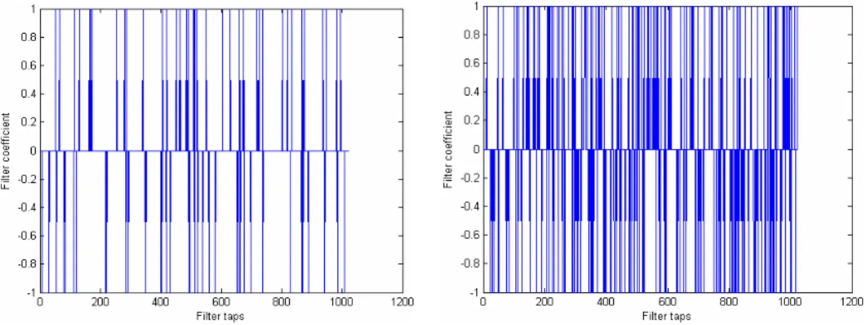
(30) y( j ) = y( j − 1) − [h(2i) ⋅ x(delay)] , 0 ≤ i ≤ 1024 ,. ⎧ block − (2i − j ), if j < 2i delay = ⎨ , otherwise ⎩ j − 2i,. (2.2). (2.3). where block represents the length of a spatial circular buffer, and j is equal to block. The spatial buffer is larger than the FIR order. Due to random coefficients, sound reflections can be represented by impulse responses from any direction in a room. The pseudo-random coefficient is generated by. h (i )=floor ((1 + p ) ⋅ rand (1, Le ) -p/ 2 ) ,. (2.4). where the parameter p is equal to 2×(the density of non-zero filter taps)/(sampling rate (Hz)) and Le=ceil(sampling rate × reverb time). These two signals (p and Le) indicate the probability of non-zero filter taps and the length of FIR filter (in samples), respectively. We use two different densities per second of non-zero filter taps, 1.92s reverb time, and 44,100Hz sampling rate to generate the FIR coefficients shown in Fig. 2-7. The generated sound quality and effect using coefficients in Fig. 2-7(right) are better than those of Fig. 2-7(left). These coefficients are only 0, 1, and -1. For a multi-tap FIR implementation, it can reduce MAC operations and even not need multiplication. To avoid too large accumulated values, a shifting operation is added into Eq. (2.2) after multiplication as. y ( j ) = y ( j − 1) − [h(2i ) ⋅ x(delay)] / 32 ,. 0 ≤ i ≤ 1024 .. (2.5). In order to simply design complexity for implementing reverberation, hence, we reduce FIR orders and the numbers of comb filters. The FIR filter uses pseudo-random coefficients sequence of 1's, 0's, and -1's, and the tap is less than 1024 orders. We recommend that Schroeder proposed the architecture of four-parallel comb filters and. 16.
(31) two-cascade all-pass filters as the implementing method on hardware.. Fig. 2-7. The un-weighted pseudo-random FIR sequence of 1's, 0's, and -1's with 4,000 (left) and 14,400 (right) densities per second of non-zero filter taps, respectively.. 2.3 Speech Processing One of the powerful speech analyses is Linear Prediction Coding, or LPC analysis as it is commonly referred. In the LPC analysis, the short-term correlation between speech samples (formants) is modeled and removed by a very efficient short-order filter. Another equally powerful and related method is pitch estimation (PE). The long-term correlation of speech samples are analyzed in PE. A vocal tract model, as described in [30] can be estimated using LPC analysis and approximated by an all-pole filter. We shall describe briefly the ways for finding LPC coefficients and pitch information as follows.. 2.3.1 Linear Predictive Coding In order to model the time-varying nature of the speech signal whilst staying within the constraint of our LPC analysis, i.e., stationary signal, it is necessary to limit our analysis to short-time blocks of speech. This is achieved by summations over finite limits, 17.
(32) i.e.,. φ n (i, j ) = E{s(n − i)s(n − j)} = ∑ S n(m - i)S n(m - j) ,. (2.6). m. where E is the mean squared error, the waveform segment, Sn(m), is assumed to be zero outside the interval 0 ≤ m ≤ N −1, and N is the length of the sample sequence. We use the auto-correlation method to approach the interpretation of Eq. (2.6). Since, for N ≤ m ≤ N+p, we are trying to predict zero sample values (which are not actually zero), the prediction error for these samples will not be zero. Assuming that we are interested in the future prediction performance, the limits for Eq. (2.6) can then be expressed as. φ n (i, j ) =. M + p −1. ∑S. m =0. n. (m − i ) S n (m − j ),. (2.7). (m) S n (m + i − j ),. (2.8). or. φ n (i, j ) =. N −1− ( i − j ). ∑S. m=0. n. for 1 ≤ i ≤ p and 0 ≤ j ≤ p. Equation (2.8) can be reduced to the short-time auto-correlation function, as given by. φ n (i, j ) = Rn ( i − j ), for i = 1, L, p, j = 0, L, p, where Rn ( j ) =. N −1− j. ∑ S n (m)S n (m + j ). Using the auto-correlation method,. m =0. (2.9) p. ∑α φ j =1. j. n. (i, j ). can therefore be expressed as p. ∑α j =1. j. R n ( i − j ) = R n (i ), 1 ≤ i ≤ p,. or in normal matrix form given by 18. (2.10).
(33) Rn (1) L Rn ( p − 1) ⎤ ⎡α 1 ⎤ ⎡ Rn (1) ⎤ ⎡ R n ( 0) ⎢ R (1) L L Rn ( p − 2)⎥⎥ ⎢⎢α 2 ⎥⎥ ⎢⎢ Rn (2) ⎥⎥ ⎢ n = , ⎢ ⎥⎢ M ⎥ ⎢ M ⎥ M M M M ⎢ ⎥⎢ ⎥ ⎢ ⎥ Rn (0) ⎦ ⎣α n ⎦ ⎣ Rn ( p)⎦ ⎣ Rn ( p − 1) L L. (2.11). where αj represents the estimate parameters on aj , j = 1,...,p. The above matrix has the property that it is symmetrical and all elements along a given diagonal are equal, i.e., it is a Toeplitz matrix [18]. Equation (2.10) can be solved by the simple inversion of the p × p matrix; however this is not usually performed since computational errors such as finite precision tend to accumulate. By exploiting the Toeplitz characteristic, however, very efficient recursive procedures have been devised. The Levinson-Durbin’s algorithm [33] is used to compute the prediction coefficients for LPC analysis of the auto-correlation sequence of samples. It provides solutions to the linear equations through recursive procedure that exploits the symmetry property.. 2.3.2 Pitch Estimation Accurate estimation of the pitch period or the lag τ in the speech coding is very important. The direct distance measurement is the most popular criterion, examining the similarity between two waveforms which can be expressed as E (τ ) =. 1 N. 2. N −1. ∑ [s(n) − βs(n + τ )] ,. (2.12). n =0. where β is a scaling factor, or the pitch gain, controlling the changes in signal level. Under the assumption that the signal is stationary, the error criterion of Eq. (2.12) can be written as N −1. E (τ ) = [R(0) − R(τ )], where R(τ ) = ∑ s(n) s (n + τ ). n =0. 19. (2.13).
(34) Speech in the long term is a non-stationary signal, and the direct similarity criterion may exhibit large errors, implying fewer similarities in position where the shift is equal to the real pitch period. Equation (2.13) is the direct auto-correlation which indicates more similarities in triple pitch period as the amplitude is increasing. The normalized similarity criterion in Eq. (2.12) is derived under the consideration of such a non-stationary process. Setting ∂E(τ, β)/∂β = 0 of Eq. (2.12), the optimum normalization coefficient (pitch gain) can be calculated using N −1. β=. ∑ s ( n) s ( n + τ ) n =0 N −1. ∑ s 2 (n + τ ). .. (2.14). n =0. By substituting the optimum gain back into the error function of Eq. (2.12), the pitch can be estimated by minimizing 2. ⎡ N −1 ⎤ ⎢∑ s ( n) s ( n + τ ) ⎥ N −1 ⎦ . E (τ , β ) = ∑ s 2 (n) − ⎣ n =0N −1 n =0 ∑ s 2 (n + τ ). (2.15). n =0. This is equivalent to maximizing the square of the normalized auto-correlation function given by 2. ⎡ N −1 ⎤ ⎢∑ s ( n) s ( n + τ ) ⎥ ⎦ Rn2 (τ ) = ⎣ n=0N −1 . 2 ∑ s (n + τ ). (2.16). n =0. The pitch period can be determined from Eq. (2.16). The normalized auto-correlation method shows a much better performance than direct (un-normalized) auto-correlation method. 20.
(35) CHAPTER 3 DESIGN. OF. APPLICATION-DRIVEN. DIGITAL. SIGNAL PROCESSOR. 3.1 Introduction The proposed application-driven digital signal processor (DSP) [85]-[87], called LASP24 (Low-cost Application-driven Speech Processor, 24-bit data width), is constructed as a reduced instruction set computer (RISC) architecture with vector and matrix operations and power optimization. An effective verification is used to subserve the hardware design and to decrease debugging time during the development of hardware and software. High performance is achieved by vector and matrix operations that are not usually supported by general-purpose DSPs. The parallel architecture of LASP24 can quickly execute vector and matrix operations without extra overhead. High flexibility in use, small area on silicon, high data throughput, and fast portability to a wide range of technologies are our main targets in the core development. The development of the digital signal processor shown Fig. 3-1 is to meet the system demands that are based on sophisticated arithmetic algorithms and that emphasize on both hardware and software solutions. The verified tools offer the opportunity to trade off between software (for flexibility) and hardware (for performance and power optimization). The development flow consists of two parts: hardware implementation and software development. Software includes two development tools: the assembler and the emulator. The assembler can translate assembly language into binary codes (or called machine codes). Simultaneously, the initial ROM file is generated for the processor emulator and the HDL 21.
(36) simulator. The emulator can emulate the computations of the processor hardware and verify the precision of different floating-point formats such as 32- or 24-bit. In hardware design, using the hardware description language (HDL) implements the processor and improves performance and power dissipation for speech/audio algorithms. The processor can be regarded as an embedded DSP processor.. Fig. 3-1. Hardware/Software development flow for LASP24.. 3.2 Micro-architecture The RISC-type [31] processor has traditionally enhanced performance by the reduced instruction set to maximize the throughput, and most of them access rather a large program memory at every clock cycle to fetch each instruction. Thus, application-driven design can reduce complexity and is greatly enhanced at performance. For an embedded DSP, it is necessary that the architecture should support effective data communication between memory system and execution units, low-overhead loop control, and accumulator-based 22.
(37) instruction set architecture. An efficient method of data representation and a hardware implementation is proposed to utilize a smaller program memory, while maintaining other merits of the RISC, such as simple decoding, fixed instruction size, and high performance. LASP24 is a 24-bit DSP processor with a floating-point unit and is ease of use. The DSP processor has the architecture of a 24-bit single-instruction/multiple-data (SIMD) instruction set with five addressing modes, and a five-level pipeline executing engine, which is Instruction Fetch (IF), Instruction Decode (ID), Execution (EX1, EX2), and Write Back (WB). It is important to perform parallel multiplication and arithmetic operations in a single cycle. This allows instruction execution to overlap. Thus, the effective execution time for most instructions is one cycle. Some key features of LASP24 are listed below: z. 24-bit fixed length instructions which support 2- and/or 3-operand.. z. Five pipeline stages to improve throughput.. z. Five addressing modes and one control mode. Up to the support of 32 instructions.. z. Two bank internal memories for use of vector addressing.. z. 24 address stacks and 70 data stacks.. z. Block repeat capability.. z. Zero-overhead loops with a single-cycle branch.. z. Branch conflict with hardware detection and solution.. z. Power saving consideration.. Floating-point operations provide fast, accurate, and precise computations. The 24-bit floating-point format is compatible with IEEE-754 standard [32]. Specifically, LASP24 facilitates floating-point operations at high speed for speech/audio signal processing, which offers addition, subtraction, multiplication, and simulated division. 23.
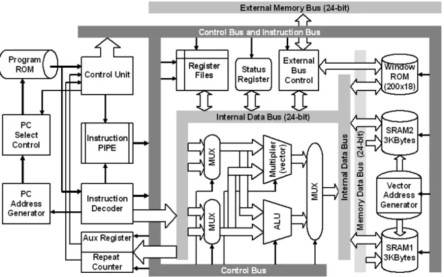
(38) The block diagram of proposed LASP24 is shown in Fig. 3-2. LASP24 is functionally partitioned into the following major blocks: a computation unit, which indicates ALU, multiplier, and accumulators, a program control unit, an external bus control dictating LASP24 external buses, a vector address generator computing the addresses which are used in vector operations. The program control unit performs instruction fetch, decoding, exception handling, and wait state supports. The PCU generators the next address to the program memory and controls hardware loops.. Fig. 3-2. The block diagram of the proposed digital signal processor. LASP24 includes four register groups. The eight general-purpose registers (Register File) are capable of storing and supporting operations on 24-bit floating-point numbers. The two 8-bit auxiliary registers can be accessed by the processor and modified by the auxiliary register arithmetic unit. The primary function of the auxiliary registers is the generation of 8-bit addresses. They can also be used as loop counters or as matrix point register. The status registers contain information relating to the state of ALU and parallel multiplication. When the status registers is loaded, LASP24 sends out a busy signal, and 24.
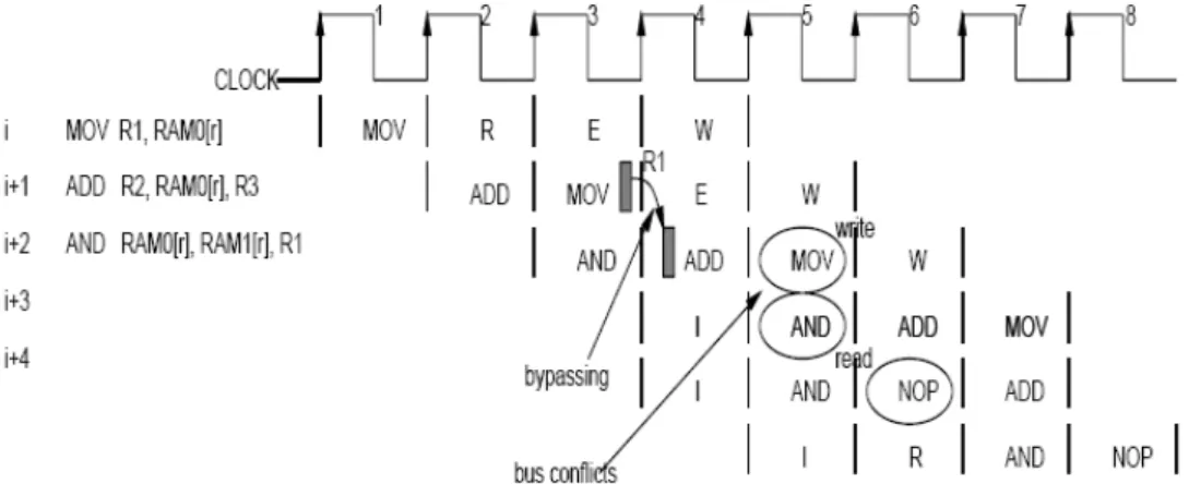
(39) executes the selected function. The two 8-bit repeat counters which used to specify the number of times are to be repeated when performing a block repeat. LASP24 uses a five-stage pipelined structure, and the pipelined operation is shown in Fig. 3-3. The Instruction Fetch (I) stage fetches the instruction words from instruction ROM and updates the program counter (PC). The Read and Decode (R) stage decodes the instruction word and performs address generation. Also, it controls the modification of the AR0 and AR1 registers in the matrix and vector addressing modes, and if required, reads the operands from memory or general registers. The Execution (E) stage is divided into two stages and performs the necessary operation, such as floating-point addition, subtraction and multiplication. The Write Back (W) stage, if required, writes results to the register file and memory.. Fig. 3-3. Pipelining operations. The pipelined control exists the problems of conflicts (or hazards). The conflicts can be grouped as branch, memory, and register conflicts. The branch and register conflicts are described in [58], and the concept of its solution to these conflicts is applied to our design. The register conflicts arise when an instruction depends on the results of a previous instruction in a way that is caused by the overlapping of instructions in the pipeline. Using the forwarding way can solve the problem of register conflicts. The branch conflicts arise from the pipelining of branches and other instructions that change the PC. The condition of 25.
(40) a branch conflict is shown in Fig. 3-4. The (i+2)th instruction will return to the jth instruction, but the pipeline register has fetched the (i+2)th instruction. For the branch taken, the (i+2)th instruction is not used and replaced by the “NOP” instruction. This. Fig. 3-4. Branch operations. change solves the branch conflict, but the pipeline causes overhead. Hence, we modify the way of branch conflicts in Fig. 3-4 to avoid NOP operation and to reduce time overhead. The branch conflict in LASP24 does not exist because the PC is changed in the I stage and the R stage, not in the E stage. Before the next cycle, the indicated branch instruction will be ready in the I stage. That means the program control is free of branch conflicts, and there is zero overhead for a branch instruction. The memory conflicts arise from resource conflicts when the hardware cannot support all possible combinations of instructions in the simultaneous overlapping. As shown in Fig. 3-5, this type of conflicts may happen. The ith instruction does not yet write R1 to the location of RAM0[r], but the (i+1)th instruction reads data from the location of RAM0[r]. At this time, a memory hazard occurs in the pipeline. The (i+2)th instruction is reading data from the locations of RAM0[r] and RAM1[r], but the ith instruction is writing R1 to RAM0[r]. This is seriously conflicts for memory data buses. The solution is to assign the priority of writing memory higher than. 26.
(41) that of reading. The above condition similarly occurs between two internal RAMs and one external bus. In the other way, the software codes can also avoid this type of conflicts.. Fig. 3-5.. Memory accessing operations.. 3.3 Instruction Set The processor instruction sets have been designed with two goals in mind: 1) to make maximum use of the processor’s underlying hardware, thus increasing efficiency and 2) to minimize the amount of memory space required to store DSP programs, since DSP applications are often quite cost-sensitive and the cost of memory contributes substantially to overall chip and/or system cost. To accomplish these two goals, it is necessary to reduce the number of bits required to encode instructions and to offer fewer registers and addressing modes than other types of processors. Thus, the architecture of LASP24 is defined as a fixed instruction length at 24 bits. A 24-bit instruction uses five bits each for addressing 8 general-purpose registers. LASP24 instruction set includes five addressing modes and is classified into three groups as data transfer, arithmetic, and control instructions. The total of defined instructions is about twenty-five (see Appendix A in details). Some representative instructions are listed as follows.. 27.
(42) Instruction. Descriptions and Examples Load and Store Instructions. MOV. LD. Load, store and move data 1. General data moves EX: MOV RAM0[address], R0; R0=RAM0[address] 2. Data moves for the matrix addressing mode EX: MOV RAM1[AR1L+1, AR0L], R3; R3=RAM1[AR1L+1, AR0L], where AR0L and AR1L are defined as AR0[3:0] and AR1[3:0]). Load fixed values as follows: 0.0, 0.75, 1.0, and 2.0 - A (the floating-point value from 2.0 leaves operand A). Arithmetic Instructions ADD SUB MPY. VMPY MAC DIVEXP NORM. Add floating-point values EX: ADD R0,R1,R2; R2=R1+R0 Subtract floating-point values EX: SUB R0,R1,R2; R2=R1-R0 1. General multiplication EX: MPY R0,R1,R2; R2=R1×R0 2. Matrix multiplication EX: MPY R3,RAM0[1110,AR0L-AR1L]; R3=RAM0[1110,AR0L-AR1L]×R3 Vector multiplication EX: VMPY EXT[j],WIN[j],RAM0[j],RAM1[j]; {RAM0[j],RAM1[j]}=EXT[j]×WIN[j] Multiplication-and-accumulation EX: MAC RAM0[j], RAM1[j], R3; R3=RAM0[j]×RAM1[j]+ACC, where ACC is an accumulator. Re-scale after division EX: DIVEXP R0,R3; R3=DIVEXP(R0) Normalize floating-point value EX: NORM R0,R1; R1=Norm(R0). Program Control Instructions NOP LDC RPB RETB END. No operation Load AR0 and AR1 value EX: LDC AR0,#14; load 14 to AR0 Begin repeat block EX: RPB RC0, 255; for (r=0; r<=254; r++) Return repeat block of instruction EX: RETB AR0, label; if AR0=RC0, goto label End of programs (halt). 3.3 Addressing Modes Most of speech and audio processing is related with auto-correlation, convolution, and FIR calculation. Hence, addressing modes are to enhance the hardware computing. 28.
(43) capability for the algorithms. Five types of addressing modes allow access of data and instruction words from memory and registers: register, direct, indirect, immediate, and vector addressing modes. These detailed addressing formats are described in Appendix B. The register addressing mode offers internal accessing operations of general-purpose registers. In this addressing mode, an ALU register contains three operands, as shown in this general operation: “RA Operation RB ⇒ RC.” The destination operand is RC and the source operands are RA and RB. The direct addressing mode offers an immediate value as an index of memory address to access memory data. In this addressing mode, the data address is formed by 0-7 bits in the instruction. Because the length of instruction is short, the direct addressing mode only supports RAM block 0. The matrix addressing mode is designed for Durbin's algorithm [33] and used to compute matrix multiplication. For example, there is a 10×10 matrix multiplication. To access data in the matrix fast, the auxiliary registers (AR0 and AR1) are used to assist addressing the coordinate (X, Y) in the matrix. In matrix addressing, a three-operand instruction can be used in the indirect addressing mode. The vector addressing mode is used in data computation between memory and memory. This mode provides 512-data-length vector operations and can also execute parallel instructions that make auto-correlation function operate faster than the general-purpose DSPs. Additionally, a control mode is defined to control data paths in the processor design. Programmers can use this mode to control their program flow and/or to easily set of repeat counters. Through two auxiliary registers (AR0 and AR1), the processor can execute two-level nested program. The function-finishing instruction and holding status are also in the control mode. The loop control is very useful for auto-correlation function in Durbin's algorithm [33] because they are all two-level nested programs. The mode is very efficient to handle the program flow without any additional instructions, which might be necessary. 29.
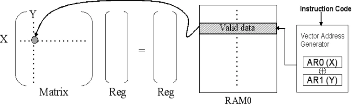
(44) to other general-purpose DSPs.. 3.4 Matrix Processing Technique Particularly, we design an auto-index method which uses auxiliary registers to address memory data as shown in Fig. 3-6. This method called matrix addressing can easily get memory data in a single multiplier instruction. When the instruction decoder gets the vector address, the address would represent the coordinate of the matrix. Matrix multiplication is based on the operation of RAM0 and R3 (the third general-purpose register). The results are stored to the R3 register. An example for the equation of matrix multiplication is as. y=. 0. ∑ x[k , r − j]h[ j + 1, r ] .. (4.1). j = r −1. We can replace the above with the following LASP24 micro codes: RPB j, #r-1 L1: MOV WIN[j+1, r], R3; MPY R3, RAM0[AR0, r-j], R3 ADD R1, R3, R1 RETB j, L1. // set repeat block counter // move a coefficient to R3 // matrix multiplication // R1=R1+R3 // if j≠0, return to L1. The index of a matrix coordinate is defined by auxiliary registers (AR0 and AR1). The address index can automatically increase so that the pointer indicates the next matrix address. Hence, this addressing method enables a single-instruction matrix computation so that the size of program memory and the number of program memory access can be reduced.. 30.
(45) Fig. 3-6. Illustration for computing a matrix address with the vector addressing mode. In Fig. 3-6, the instruction decoder gets the matrix position with four bits listed in Table 3-1 and then transfers them to the address processing unit. The processing unit can analyze and calculate the matrix address (X, Y) in RAM0. Table 3-1 shows the coordinate table of two matrix addressing modes. One is the indirect addressing mode as RAM0[AR0]; the other is the matrix addressing mode as RAM0[AR0L+1, AR0L+1]. The matrix coordinate is defined in AR0 and AR1. The index automatically adds one so that the pointer indicates the next matrix address. The vectors {0000, 0001} and {1110, 1111} are two special coordinates which can directly access the start and the end of row location in the matrix. Hence, the proposed matrix addressing method enables a single-instruction matrix computation so that the total number of program instructions can be reduced. Table 3-1.. CODE. The matrix coordinate for the matrix addressing mode, where AR0L and AR1L represent the lower four bits of AR0 (AR0[3:0]) and ar1 (AR1[3:0]), respectively. Addressing Mode. CODE. Addressing Mode. 0000. RAM0[AR0]. 1000. RAM0[AR0L-AR1L, AR0L]. 0001. RAM0[AR1]. 1001. RAM0[AR1L+1, AR0L+1]. 0010. RAM0[AR0+AR1]. 1010. Reversed. 0011. RAM0[1111, AR0L]. 1011. Reversed. 0100. RAM0[AR1L+1, AR0L]. 1100. RAM0[0000, AR0L]. 0101. RAM0[1110, AR0L-AR1L]. 1101. RAM0[1110, AR0L]. 0110. RAM0[1110, AR0L+1]. 1110. Reversed. 0111. RAM0[AR0L+1, AR0L+1]. 1111. RAM0[0001, AR0L]. 31.
(46) 3.5 Vector Processing Technique The SIMD-style vector processing scheme provides an approach to accelerating the processing of data streams. This technique can provide a significant speedup for communications, multimedia, and other performance-driven applications by using data-level parallelsim. In the vector processors [34], [35] the design can provide high-level operations that work on vectors - linear arrays of numbers. The vector processing unit supports both intra- and extra-memory operations. In the operation, elements work in parallel on the corresponding elements from multiple intra- or extra-memory sources and place the results in the corresponding fields in the destination operand memories. An operation example is the vector multiplication (VMPY) instruction shown in Fig. 3-7, and the instruction format and addressing representation are shown in Table 3-2.. VA (Source Memory 1). .......... .......... OP. OP. VB (Source Memory 2). OP. OP. ............ Fig. 3-7.. VC (Destination Memory). An example of memory operations in LASP24, where OP indicates the vector multiplication. VA, VB, and VC represent different memory banks. They are defined in Table Table 3-2.. 32.
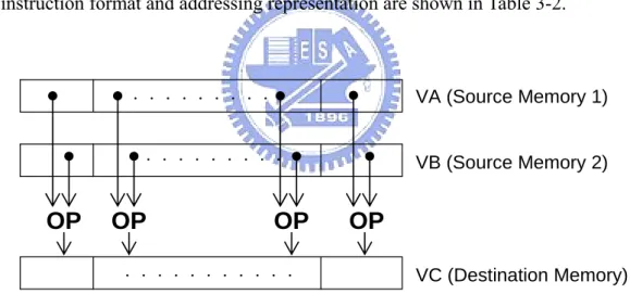
(47) Table 3-2.. The format of the vector addressing mode and the representation of vector addresses in LASP24, where OP indicates operation; VA, VB, and VC represent vector registers. The symbols, FIL, EXT, WIN, RAM0, and RAM1, are memory symbols.. VC ⇐ VA[AR_A] OP VB[AR_B] 23 ~ 19. 18~16. 15~14. OPCODE. 011. NU. 13~12 11~10 FIL. EXT. 9~8. 7 ~6. 5~4. 3~2. 1~0. RAM0. RAM1. VC. VA. VB. FIL. EXT. RAM0. RAM1. VC. VA. VB. VL. 13~12. 11~10. 9~8. 7~6. 5~4. 3~2. 1~0. 00. FIL. EXT. AR0. AR0. RAM0. RAM0. RAM0. AR1. AR1. RAM1. RAM1. RAM1. EXT. EXT. WIN. R3. -. FIL. 01. FIL+AR0 EXT+AR0. 10. FIL+AR1 EXT+AR1 AR0+AR1 AR0+AR1. 11. FIL-AR0. EXT-AR0. AR1-AR0. AR1-AR0. The vector multiplier has several important properties that solve most of the above problems as explained below. 1. The computation of each result is independent of the computation of previous results, allowing a pipelined operation without generating any data hazards. 2. A single vector instruction specifies a great deal of computation work. It is equivalent to executing an entire loop. Thus, the number of instruction fetch is reduced, and the bottleneck is considerably mitigated. 3. The vector instruction has a known memory access pattern. If the vector's elements are all adjacent, then fetching the vector from a set of heavily interleaved memory banks works very well. The high latency of initiating a main memory access versus accessing an instruction ROM is rather high, because a single access is initiated for the entire vector rather than for a single element. Thus, the cost of the latency to memory is seen only once for the entire vector, rather than once for each element of the vector.. 33.
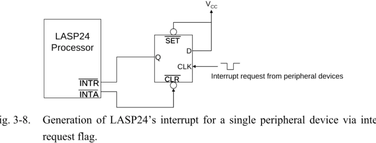
(48) 4. Because an entire loop is replaced by a vector instruction whose behavior is predetermined, control hazards that would normally arise from the loop branch are nonexistent. To illustrate the above features, we compare performance with a general-purpose DSP in computing the vector multiplication of 100 points. A vector multiplication instruction fetches data from RAM0 and RAM1 and feeds into ALU. ALU executes the “MAC” operation and adds the result to the accumulating register. The final results are stored to the external memory. An example of vector processing (100 points) is shown as follows. L1: MPY RAM0(r), RAM1(r), EXT(r); RETB r, L1. // EXT(r)= RAM0(r)× RAM1(r) // r=r+1. if r=100, then jump to L1. The total execution time is about 200 clock cycles. Hence, we use a single instruction within a repeat block to execute the parallel multiplication-and-accumulation in the auto-correlation operation. The above example demonstrates that LASP24 has higher performance in vector computation than the general-purpose DSPs such as the TI TMS320C3X series.. 3.6 DMA and Interrupt Interface LASP24 needs the interrupt and direct memory access (DMA) to process data transformation. The interrupt is to tell LASP24 that peripheral devices are to be active. DMA is to free the bus control and to deal with the operation of I/O-to-memory or memory-to-memory data moving. There is a control interface for interrupt and DMA. We take advantage of a simple finite state machine (FSM) to implement its circuit. Each state. 34.
數據
+7
相關文件
` Sustainable tourism is tourism attempting to make a low impact on the environment and local culture, while helping to generate future employment for local people.. The
In this thesis, we have proposed a new and simple feedforward sampling time offset (STO) estimation scheme for an OFDM-based IEEE 802.11a WLAN that uses an interpolator to recover
In this thesis, we develop a multiple-level fault injection tool and verification flow in SystemC design platform.. The user can set the parameters of the fault injection
The purpose of this thesis is to propose a model of routes design for the intra-network of fixed-route trucking carriers, named as the Mixed Hub-and-Spoke
Singleton,”A methd for computing the fast Fourier Transform with auxiliary memory and limited high-speed storage”, IEEE Trans. Audio
This thesis makes use of analog-to-digital converter and FPGA to carry out the IF signal capture system that can be applied to a Digital Video Broadcasting - Terrestrial (DVB-T)
This thesis adopts GUI (Graphic User Interface ) user's figure interface method, to created a figure interface that integration testing, correspondent with the change that digital
Hence this study uses a systematic method to develop safety evaluation indices and their weights to evaluate the walking environment of way to school for
