國 立 交 通 大 學
電子工程學系 電子研究所碩士班
碩 士 論 文
具有超薄
N
2
O 退火氮化物閘極介電層與
矽鍺通道之金氧半場效電晶體可靠度及
通道厚度效應研究
A Study of Reliability and Channel
Thickness Effect on Si
0.85
Ge
0.15
MOSFETs
with Ultra-Thin N
2
O-annealed Nitride
Gate Dielectric
研 究 生:陳 怡 誠
指導教授:張 俊 彥 博士
具有超薄
N
2O 退火氮化物閘極介電層與矽鍺通道之
金氧半場效電晶體可靠度及通道厚度效應研究
A Study of Reliability and Channel Thickness Effect
on Si
0.85Ge
0.15MOSFETs with Ultra-Thin
N
2O-annealed Nitride Gate Dielectric
研 究 生:陳 怡 誠
Student:Yi-Cheng Chen
指導教授:張 俊 彥 博士 Advisor:Dr. Chun-Yen Chang
國 立 交 通 大 學
電子工程學系 電子研究所碩士班
碩 士 論 文
A Thesis
Submitted to Department of Electronics Engineering & Institute of Electronics
College of Electrical Engineering and Computer Science
National Chiao Tung University
in partial Fulfillment of the Requirements
for the Degree of
Master
in
Electronics Engineering
June 2004
Hsinchu, Taiwan, Republic of China
具有超薄
N
2O 退火氮化物閘極介電層與矽鍺通道之
金氧半場效電晶體可靠度及通道厚度效應研究
研 究 生:陳 怡 誠 指 導 教 授:張 俊 彥 博士
國立交通大學
電子工程學系 電子研究所碩士班
摘
要
在本論文中,我們針對具有矽鍺(Si
0.85Ge
0.15)通道與超薄 N
2O 退火氮化
物閘極介電層(等效氧化層厚度約 3.1 奈米)之金氧半場效電晶體進行可靠度
與通道厚度效應的研究。根據經驗公式,在矽基板與矽鍺通道接面處的價
帶能階偏移量大約是
0.1 電子伏特,而閘極電流的傳導機制則主要是等效位
能障約
1.8 電子伏特的 FN 穿遂機制。經過定電壓壓迫(CVS)及定電流壓迫
(CCS)後,我們發現對 N
2O 退火之矽化氮(SiN)閘極介電層並沒有造成明顯
的損害,不過卻觀察到與電壓極性相關之電應力導致的漏電流(SILC),此現
象 可 藉 由 陽 極 電 洞 注 入
(AHI) 模 型 加 以 解 釋 。 隨 後 我 們 進 行 熱 載 子
(hot-carrier)壓迫以及負電壓溫度產生不穩定性(NBTI)的電性量測,藉以評估
矽鍺通道之
p 型金氧半場效電晶體的可靠度。在負電壓溫度產生不穩定性
的壓迫下,我們已顯示電子缺陷(electron trapping)主導元件效能的破壞程
度,而在熱載子壓迫的情況下則是由壓迫產生的界面狀態造成主要損害。
由於電荷拉推電流(charge pumping current)的結果顯示 V
g=V
d之壓迫產生最
多的界面狀態,因此對於具有矽鍺通道及
N
2O 退火矽化氮閘極介電層之 p
型金氧半場效電晶體的可靠度問題,我們認為
V
g=V
d之壓迫情況導致元件效
能最嚴重的損傷。另一方面,矽緩衝層的不完美晶格引起高密度錯排
(dislocation),並且降低驅動電流、轉導(transconductance)及等效載子遷移
率,因此我們提出無矽緩衝層的矽鍺通道金氧半場效電晶體具有較佳的元
件特性。此外,搭配
5 奈米和 15 奈米厚度的矽鍺通道金氧半場效電晶體,
除了次臨界電壓振動(swing)低到 67 mV/A,與 30 奈米矽鍺通道的元件相
比,還具有較高的驅動電流、較低的界面狀態密度、較低的漏電密度、較
高的轉導和較佳的等效載子遷移率。最後,對於未來次
100 奈米的技術領
域,我們證明搭配矽鍺通道及
N
2O 退火矽化氮閘極介電層之金氧半場效電
晶體將具有高度的潛力。
A Study of Reliability and Channel
Thickness Effect on Si
0.85
Ge
0.15
MOSFETs
with Ultra-Thin N
2
O-annealed
Nitride Gate Dielectric
Student: Yi-Cheng Chen Advisor: Dr. Chun-Yen Chang
Department of Electronics Engineering and Institute of Electronics
National Chiao Tung University
ABSTRACT
We have investigated the reliability and the channel thickness effect of MOSFETs with Si0.85Ge0.15 channel and ultra-thin (EOT=3.1 nm) N2O-annealed SiN gate dielectric. The offset
of valence band is about 0.1 eV. The FN tunneling dominates the conduction mechanism of the gate current with an effective barrier height of 1.8 eV. In addition, the results of CVS and CCS stressing show the insignificant degradation of the N2O-annealed SiN gate dielectric,
and the polarity dependent SILC has been observed and explained by anode hole injection (AHI) model. The hot-carrier (HC) stressing and negative bias temperature instability (NBTI) are performed to evaluate the reliability of the SiGe channel pMOSFETs. We have
demonstrated that electron trapping dominates the device degradation for the NBTI stressing and the interface state generation is dominant mechanism for the HC stressing. The results of the charge pumping current have shown the highest interface state density are generated after the device being stressed at Vg=Vd. Therefore, the stressing condition of Vg=Vd has been
considered as the worst case for evaluating the reliability of the SiGe channel pMOSFET with N2O-annealed SiN gate dielectric. Because of the high dislocation density induced by the
imperfect crystalline Si buffer layer, the driving current, transconductance, and effective mobility are degraded. Therefore, the SiGe channel MOSFETs without a Si buffer layer is proposed to have better device performance. Moreover, the MOSFETs with 5 and 15 nm SiGe channel have been shown smaller subthreshold swing of 67 mV/A, higher driving current, lower interface state density, lower leakage current, larger transconductance, and greater effective mobility as compared with the 30 nm SiGe channel devices. Finally, the MOSFETs with thin SiGe channel and N2O-annealed SiN gate dielectric have been demonstrated their
誌 謝
在短短兩年的碩士班研究生涯,首先感謝指導教授 張俊彥校長,在
繁忙的校務工作之餘仍耐心地給予實驗室學生們學術上的指導與勉勵,而
老師寬懷的胸襟與遠見更是我們應當學習的目標。其次感謝國家奈米實驗
室之研究員 簡昭新博士,其認真的研究態度與豐富的知識,令學生受益
匪淺。也感謝國家奈米實驗室裡的工程師與實驗群,由於他們在實驗上的
支援才得以完成學生的作品。
此外,特別感謝陳經緯學長,不僅解答課業、實驗上的疑問,於日常
生活中亦不斷地鼓勵我上進,導正人生態度,如果沒有陳經緯學長的傾囊
相助,我也無法獨力完成碩士論文。也謝謝實驗室裡的學長與同屆畢業的
王凱立、林慶宗、胡嘉欣與胡心卉同學,陪我一同走過兩年的碩士生活,
留下許多快樂的回憶。
最後,我要特別感謝親愛的父母以及家人,感謝你們辛苦的栽培及默
默付出,使得我得以全心投入學業。
Contents
ABSTRACT (Chinese) --- Ⅰ
ABSTRACT (English) --- Ⅲ
Acknowledgement --- Ⅴ
Contents --- Ⅵ
Figure Captions --- Ⅷ
Chapter 1 Introduction
1-1 Background --- 1
1-2 Motivation ---
3
1-3 Organization of the Thesis --- 4
Chapter 2 Experiment
2-1 Device Fabrication Process --- 6
2-2 Electrical Characteristics Measurements ---
7
Chapter 3 Reliability of 50 nm Si
0.85Ge
0.153-1 pMOSCAP --- 9
3-2 pMOSFET --- 11
Chapter 4 Channel Thickness Effect on
Si
0.85Ge
0.15MOSFETs
4-1 SiGe MOSFETs with and without Si buffer layer --- 14
4-2 MOSFETs with 5, 15 and 30 nm SiGe Channel --- 16
Chapter 5 Conclusion --- 20
References --- 23
Figures --- 29
Figure Captions
Fig. 2-1 Device process flow.
Fig. 2-2 The structure of the Si0.85Ge0.15 channel MOSFETs.
Fig. 3-1 The band diagram of the Si0.85Ge0.15 channel device under the inversion
condition.
Fig. 3-2 The electrical characteristics of the pMOSCAP with 50 nm Si0.85Ge0.15 channel
and N2O-annealed nitride gate dielectric. (a) The capacitance versus gate
voltage. (b) The gate current density versus gate voltage.
Fig. 3-3 The fitting of the FN tunneling with an effective barrier height of 1.8 eV.
Fig. 3-4 The normalized capacitances measured under constant voltage stress (CVS). (a) The characteristics of capacitance-voltage (C–V) with CVS time. (b) The hysteresis after –5 V stressing for 3000 seconds.
Fig. 3-5 The normalized capacitances measured under constant current stress (CCS). (a) The characteristics of capacitance-voltage (C–V) with CCS time. (b) The hysteresis after –5 V stressing for 3000 seconds.
Fig. 3-6 The characteristics of current-voltage (I–V) related to (a) CVS time and (b) CCS time.
Fig. 3-8 The electrical characteristics of Si0.85Ge0.15 channel pMOSFET with 50 nm
Si0.85Ge0.15 channel and N2O-annealed nitride gate dielectric. (a) The Id–Vg
curves. (b) The Id–Vd curves.
Fig. 3-9 The effects of HC and NBTI on pMOSFET with Si0.85Ge0.15 channel. (a) The Id
degradation versus stress time. (b) The Gm degradation versus stress time.
Fig. 3-10 The characteristics of threshold voltage shift versus stress time under different
stress conditions.
Fig. 3-11 (a) Compare of charge pumping current before and after stress. (b) Compare of
charge pumping current displayed in small scale.
Fig. 3-12 The interface state densities generated by three stress conditions at stressing
voltage of –5 V, which are calculated from the charge pumping current.
Fig. 3-13 The lifetime extracted from (a) Id degradation and (b) Gm degradation.
Fig. 3-14 The stressing conditions of Vg=Vd. (a) The Id degradation and (b) the Gm
degradation versus stress time under –4.5, –5 and –5.3 V stressing.
Fig. 3-15 The threshold voltage shifts by the stressing conditions of Vg=Vd.
Fig. 4-1 The C–V characteristics of (a) pMOSCAPs and (b) nMOSCAPs with and without the 10 nm Si buffer layer under Si0.85Ge0.15 channel. The control
samples are the conventional Si channel devices.
Fig. 4-2 The Id–Vg characteristics of (a) pMOSFETs and (b) nMOSFETs with and
swings are small to 66~68 mV/A. The control samples are the conventional Si channel MOSFETs.
Fig. 4-3 The Id–Vd characteristics of pMOSFETs (left part) and nMOSFETs (right part)
with and without the 10 nm Si buffer layer under Si0.85Ge0.15 channel. The
control samples are the conventional Si channel devices.
Fig. 4-4 The transconductance of (a) pMOSFETs and (b) nMOSFETs with and without the 10 nm Si buffer layer under Si0.85Ge0.15 channel. The control samples are the
conventional Si channel devices.
Fig. 4-5 (a) The effective hole mobility of pMOSFETs, and (b) the effective electron mobility of nMOSFETs.
Fig. 4-6 The interface state density of (a) pMOSFETs and (b) nMOSFETs from charge pumping technique. The relation between subthreshold swing and device structure has also been plotted.
Fig. 4-7 The measured gate induced drain leakage (GIDL) of (a) pMOSFETs and (b) nMOSFETs with and without the 10 nm Si buffer layer under Si0.85Ge0.15
channel. The control samples are the conventional Si channel MOSFETs.
Fig. 4-8 The junction leakage of (a) pMOSFETs and (b) nMOSFETs with and without the 10 nm Si buffer layer under Si0.85Ge0.15 channel.
Fig. 4-9 The C–V characteristics of (a) pMOSCAPs and (b) nMOSCAPs with different SiGe channel thickness. All the MOSCAPs have no 10 nm Si buffer layer under
the Si0.85Ge0.15 channel.
Fig. 4-10 The Id–Vg characteristics of (a) pMOSFETs and (b) nMOSFETs with different
SiGe channel thickness. All the MOSFETs have no 10 nm Si buffer layer under the SiGe channel. The thinner Si0.85Ge0.15 channel devices have smaller
subthreshold swings.
Fig. 4-11 The Id–Vd characteristics of pMOSFETs (left part) and nMOSFETs (right part)
with different SiGe channel thickness. All the MOSFETs have no 10 nm Si buffer layer under the Si0.85Ge0.15 channel.
Fig. 4-12 The interface state density of (a) pMOSFETs and (b) nMOSFETs with different
Si0.85Ge0.15 channel thickness from charge pumping technique.
Fig. 4-13 The measured GIDL of (a) pMOSFETs and (b) nMOSFETs with different SiGe
channel thickness. All the devices have no 10 nm Si buffer layer under the Si0.85Ge0.15 channel.
Fig. 4-14 The junction leakage of (a) pMOSFETs and (b) nMOSFETs with different SiGe
channel thickness.
Fig. 4-15 The transconductance of (a) pMOSFETs and (b) nMOSFETs with different
SiGe channel thickness. All the MOSFETs have no 10 nm Si buffer layer under the Si0.85Ge0.15 channel.
Fig. 4-16 (a) The effective hole mobility of pMOSFETs, and (b) the effective electron
Chapter 1
Introduction
1-1 Background
So far, increasing the inversion gate capacitance, enhancing the carrier transport, enhancing the immunity of shorter channel effect, and reducing parasitic capacitances and parasitic resistances are the most useful techniques to improve the device performance of the metal oxide semiconductor field effect transistors (MOSFETs) [1]. For example, the high-k gate dielectric can be used to induce a larger inversion charge density at the same gate bias because of its high dielectric constant, and the silicidation of source/drain can decrease the parasitic capacitance and resistance. Although, many methods have been proposed to achieve these purposes, it still needs new materials and new structures to realize the device performance enhancement.
According to the issues mentioned above, silicon germanium (SiGe) is introduced to be the channel of MOSFETs for improving carrier transport because of its higher bulk carrier mobility than the conventional Si channel devices. Moreover, the SiGe layer can be selectively deposited on the Si substrate by a chemical vapor deposition (CVD) system, and the process of device fabrication can be simplified. The offset of valence band between SiGe
and the Si will lead to the quantum confinement effect of holes [2]. Thus the hole mobility can be obviously increased for the p-type MOSFETs (pMOSFETs) with SiGe channel [3]-[5]. Besides, hole mobility will also be improved simultaneously because the compressive strain of SiGe layer is formed when SiGe is deposited on the Si substrate [6]-[10]. Furthermore, the low thermal budget process can be performed because of the high dopant solubility of SiGe which lowers the dopant activation temperature.
Unfortunately, the lattice mismatch raises with increasing the contents of Ge and it results in the increase of the dislocation density and impurity scattering in SiGe films [2]. On the other hand, if the gate oxide is formed by oxidizing the SiGe layer with conventional oxidation process, Ge atoms will be precipitated at the interface between SiGe and oxide, and meanwhile the quality of oxide will also be deteriorated [11]. Therefore, the using of Si capping layer and the gate oxide grown by deposition will be the most appropriated methods for fabricating devices with SiGe channel. However, the high temperature oxidation process of Si capping layer will probably induce the relaxation of the SiGe under layer. Additionally, because the temperature of depositing a gate oxide is lower than that of the oxidation, the thermal budget of the process can be lowered to prevent the relaxation of the strained SiGe layer. Recently, silicon nitride (SiN) has been reported as the possible alternative of gate dielectrics for MOSFETs with SiGe channel [11][12]. SiN not only has a larger dielectric constant but also can suppress the boron penetration from p+ poly-Si gate into Si substrate.
that of the Si-H bonds, SiN has been shown better hot-carrier (HC) hardness than that of silicon dioxide (SiO2) [16]. However, SiN film will induce oxide fixed charges to cause the
threshold voltage shift, and increase interface state density to degrade the device performance. Therefore, N2O-annealing has been proposed to improve the quality of SiN gate dielectric and
the SiN/Si interface [13]-[15].
1-2 Motivation
Considering the issues have mentioned above, we have fabricated MOSFET devices with SiGe channel and SiN gate dielectric. The SiN is formed by low pressure chemical vapor deposition (LPCVD) system and annealed in N2O ambience to improve the film quality.
Although many studies have been proposed on the N2O-annealed SiN film [14], SiN film as
the gate dielectric of SiGe channel MOSFETs still needs extensive investigation. Therefore, we will further study the electrical characteristics and reliability of the devices.
For conventional Si channel devices, the hot-carrier effect results in a serious reliability issue [16]. For example, the oxide trap charges and the interface state generation are caused by hot-carrier stressing [17]-[20], and then the threshold voltage and the drive capability of device will be degraded. In addition, the bias temperature instability (BTI) effect has been reported as another issue dominating the device reliability [21]-[23]. When device is stressed at high voltage and high temperature, the interface state generation dominates the degradation
of device performance because of the electrochemical reaction between the inversion charges and the interface states [24]-[26]. Therefore, we will compare the characteristics of devices after hot-carrier and BTI stressing, and discuss the mechanism of device degradation.
Finally, the relaxation is not only easily occurred when the strained SiGe deposited on the Si substrate is annealed at high temperatures [31][32], but also closely related to the strain energy in the SiGe layer. Because the amount of strain energy increases with increasing the thickness of SiGe, the thickness of SiGe channel should play an important role on the device characteristics. Thus, we will investigate the channel thickness effect on SiGe channel CMOSFETs with N2O-annealed SiN gate dielectric, and realize the optimization condition of
fabricating devices.
1-3 Organization of the Thesis
This thesis can be divided into five parts. The background of SiGe MOSFETs and the motivation of our study are introduced in Chapter 1. In Chapter 2, we describe the experimental procedures and the device structure of the SiGe channel MOSFETs with N2O-annealed SiN gate dielectric. By measuring the electrical characteristics and the
reliability of hot-carrier and BTI stressing, the mechanism of device degradation is discussed in Chapter 3. Moreover, we investigate the SiGe channel thickness effect on the fundamental characteristics of pMOSFETs and nMOSFETs. Finally, Chapter 5 presents the conclusions of
our discussion and proposes some suggestions for the potentials of SiGe channel CMOSFETs with N2O-annealed SiN gate dielectric in the future applications.
Chapter 2
Experiment
2-1 Device Fabrication Process
The Si0.85Ge0.15 channel MOSFETs with N2O-annealed ultra-thin SiN gate dielectric
were fabricated on 6-inch (100) orientated Si substrate for our experiments. The briefly device process flow was shown in Fig. 2-1. The standard local oxidation of silicon (LOCOS) process was performed to isolate the devices on the wafer. Subsequently, Si0.85Ge0.15 epitaxy layers
with various thicknesses of 5, 15, 30, and 50 nm were deposited selectively on the Si substrate by ultra-high vacuum chemical deposition system (UHVCVD) at 550 ºC. The SiGe layers were in-situ doped by phosphorus and arsenic for n-type channel and p-type channel, respectively. After being cleaned by RCA process, the ultra-thin (3 nm) SiN gate dielectrics were deposited by low pressure chemical vapor deposition (LPCVD) with dichlorosilane (DCS, SiH2Cl2) and NH3 at 780 ºC, and followed immediately by rapid thermal annealing
(RTA) at 800 ºC and 900 ºC for 30 seconds in N2O ambience. The undoped 150 nm poly-Si
deposition were performed by LPCVD with silane (SiH4) at 620 ºC and patterned by using
lithography and etching process as the gate electrode. Then, the self-aligned source/drain extension was implanted with As by a dosage of 1×1014 cm-2 at 10 keV and with BF
dosage of 1×1014 cm-2 at 10 keV for nMOSFETs and pMOSFETs, respectively. An oxide
spacer was formed by etching isotropically the LPCVD low temperature TEOS oxide (LTO), and the self-aligned gate and source/drain implantation were performed by implanting As with a dosage of 5×1015 cm-2 at 20 keV and BF2 with a dosage of 5×1015 cm-2 at 20 keV for
nMOSFETs and pMOSFETs, respectively. After the substrate contact being defined and implanted to improve the body contact, the dopant activation by RTA at 900 ºC in N2
ambience for 30 seconds was carried out. Finally, the wafers were passivated with 500 nm LTO oxide followed by a standard back-end-of-line (BEOL) contact and metallization processes, and the devices were annealed in a furnace by the forming gas at 450 ºC for 30 minutes before the electrical characteristics measurements. Figure 2-2 demonstrates the schematic device structure of SiGe channel MOSFETs with N2O-annealed SiN gate dielectric.
Moreover, the conventional Si channel MOSFETs with the same gate dielectric and device structure were also fabricated for comparing the electrical characteristics with that of SiGe channel device counterparts.
2-2 Electrical Characteristics Measurements
The high frequency (100 kHz) capacitance-voltage (C–V) characteristics of the capacitors were measured by using an Agilent 4284 LCR meter, and the EOT of gate dielectrics was determined from the strong accumulation capacitance. The current-voltage
(I–V) characteristics were measured by using Keithley 4200 semiconductor characterization system. From the Id–Vg curves, the main parameters of device, such as threshold voltage (Vt)
and subthreshold swing (S), were obtained. In addition, the density of interface state (Nit) for
MOSFETs was determined by the charge pumping current (ICP) which was measured by the
charge pumping technique. Therefore, the reliability of devices was evaluated by investigating the degradation of the device performance when they were stressed under the hot-carrier (HC) stressing and the bias-temperature instability (BTI) stressing. The channel thickness effect on the SiGe channel MOSFETs was also be studied by comparing the electrical characteristics of devices with different SiGe channel thickness.
Chapter 3
Reliability of 50 nm Si
0.85Ge
0.15pMOSCAP and pMOSFET
3-1 pMOSCAP
When SiGe is deposited directly on the Si substrate, it causes an offset of valence band (∆Ev) between SiGe and Si. Then the hole mobility is increased by the quantum confinement
effect for the pMOSFETs [2]. Figure 3-1 shows the band diagram of the devices with Si0.85Ge0.15 channel under the inversion condition. From the empirical equation of ∆Ev ~ 0.74x,
where x is the Ge mole fraction [2], the valence band offset is about 0.1 eV for Si0.85Ge0.15/Si
channel structure.
The electrical characteristics of the pMOSCAP with 50 nm Si0.85Ge0.15 channel and
N2O-annealed SiN gate dielectric is shown in Fig. 3-2. From the high frequency (100 kHz)
C–V curves as shown in Fig. 3-2(a), the equivalent oxide thickness (EOT) of 3.1 nm is
obtained by the accumulation capacitance, and no hysteresis behavior is observed. In addition, the inversion capacitance is slightly lower than the accumulation capacitance, which is mainly caused by the poly depletion effect. A low leakage current is also demonstrated in Fig. 3-2(b). When the current density is fitted by the Fowler-Nordheim (FN) tunneling, the well-fitted
straight line means that the conduction mechanism is suggested to be the FN tunneling with an effective barrier height of 1.8 eV, as plotted in Fig. 3-3.
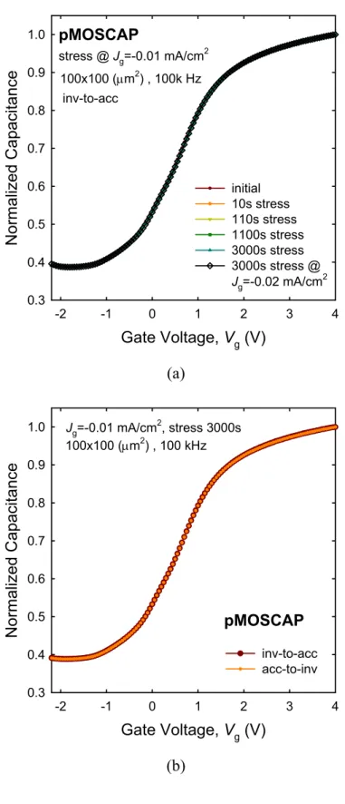
After being stressed by a constant voltage stress (CVS) at Vg = –5 V and –5.3 V up to
3000 seconds, the C–V characteristics shown in Fig. 3-4 do not be changed and show no hysteresis occurred. Similar results are also illustrated in Fig. 3-5 for a constant current stress (CCS) at Jg = –0.01 mA/cm2 and –0.02 mA/cm2 up to 3000 seconds. According to the results
of CVS and CCS, therefore, it indicates that there is almost no oxide charges generated in the N2O-annealed SiN gate dielectric during stressing. Moreover, the I–V curves after being
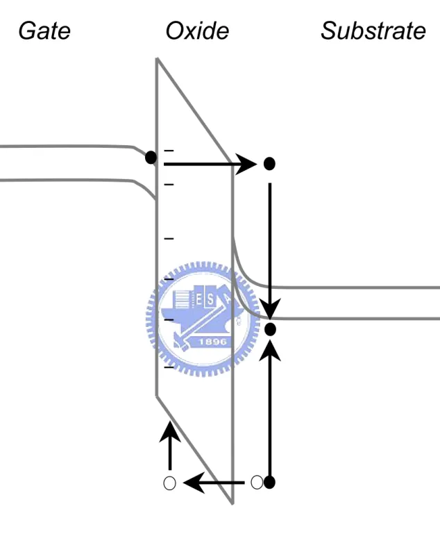
stressed by CVS and CCS are illustrated in Fig. 3-6. We find a slight increase of current density with increasing stressing time at the negative gate bias region because of the stress induced leakage current (SILC), but there is no obvious increment at the positive gate bias region. Therefore, we speculate that this polarity dependent SILC should be caused by the gate dielectric damaged by high energy holes which are generated by the anode hole injection (AHI) model in the substrate [29][30]. The schematic diagram of AHI model is demonstrated in Fig. 3-7. When electrons tunneling through the gate dielectric into the substrate by FN tunneling, the energetic electrons are produced and the impact ionization is occurred to generate the electron-hole pairs at the substrate. Then the ionized holes gain sufficient energy and are injected back to the gate dielectric, and the traps are produced near the gate electrode by the interaction between the hot holes and the gate dielectric. Therefore, even though the leakage current is enhanced by the trap-assisted-tunneling when the negative gate voltage is
applied, it is insignificant at the positive gate bias.
3-2 pMOSFET
Figure 3-8 shows the Id–Vg and Id–Vd characteristics of SiGe channel pMOSFET with
N2O-annealed SiN gate dielectric. The threshold voltage (Vt) of –1.869 V, the subthreshold
swing (S) of 124.8 mV/A, and the peak transconductance (Gm,p) of 0.11 mS are obtained from
the Id–Vg curve in the subthreshold region. Moreover, the effects of drain induced barrier
lowering (DIBL) and gate induced drain leakage (GIDL) are not found in Fig. 3-8(a). Figure 3-8(b) also displays good Id–Vd curves with various gate overdrive (Vg–Vt) voltages from 0
to –2 V.
To study the reliability of our devices, we stress the devices at different hot-carrier (HC) and negative BTI (NBTI) bias conditions. For the HC stressing, the devices are applied the voltages at Vg=Vd (Ig is maximum) and Vg=2Vd/3 (Isub is maximum) with grounded source and
substrate at room temperature. While we stress the devices under Vg = –4.5 V with grounded
source/drain and substrate at room temperature (RT) and 100 ºC for the effect of NBTI. Fig. 3-9 demonstrates the degradations of drain current and transconductance under these four stressing conditions. Obviously, the results of HC stressing show significant degradation of Id
(∆Id) and Gm (∆Gm), and the device has largest ∆Id and ∆Gm when it is stressed at Vg=Vd. On
Fig. 3-10. Interestingly, all values of ∆Vt have positive shifts for all stressing conditions. It
indicates that, therefore, electrons trapped in the gate dielectric are occurred during the stressing process. In addition, Fig. 3-10 shows that ∆Vt follows the power law in the form ∆Vt
=Atn. According to the previous report [28], a small value of n (n<0.2) means that the degradation of Vt is dominated by the electron trapping in the oxide; while for a larger value
of n (n>0.2), the mechanism of causing ∆Vt should be the interface state generation. However,
the insignificant Vt variation for the sample being stressed by NBTI at 100 ºC can be
explained by the self-recovery effect of high temperature BTI degradation [27]. Then we investigate the interface state generation by the charge pumping (CP) measurement. As shown in Fig. 3-11(a), the charge pumping currents (ICP) are increased after the devices are stressed,
and it confirms the generation of excess interface states. Again, the slightly positive shifts of
ICP shown in Fig. 3-11(b) indicate the electron trapping in the gate dielectric. Figure 3-12
compares the results of interface state generation (∆Nit) for stressing conditions of Vg=Vd,
Vg=2Vd/3, and room temperature NBTI. We can clearly see that the greatest ∆Nit has been
shown for the Vg=Vd HC stressing case. Consequently, it further indicates that generating
interface states when devices are stressed under HC stressing plays the most important role in device reliability.
The lifetimes of devices extracted from the HC degradation of Gm and Id are plotted in
Fig. 3-13. Obviously, the stressing condition of Vg=Vd shows the worse case of lifetime of Gm
stressing counterparts. However, the lifetime extracted from the ∆Id displays a reverse trend.
It can be explained as following. Figure 3-14 shows the Vg=Vd hot carrier degradations of Id
and Gm under different stressing biases verse the stress time. We can see that ∆Id and ∆Gm are
increased with the stressing voltages. However, the degradation of Gm becomes saturated
when device is stressed for a long time. It reveals that the interface state generation induced
Gm degradation may not dominate the degradation of Id for long time stressing. Meanwhile,
the variation of ∆Vt with the stress time as shown in Fig 3-15 demonstrates that when device
is stressed under higher stressing biases, the threshold voltage becomes smaller at the beginning of stressing process and then is increased sequentially toward negatively. It results in that electrons are trapped in the gate dielectric at the beginning stress time to improve the threshold voltage, but the hole trapping is occurred to further degrade the Vt with the
following stress time. Therefore, because the improvement of Vt will enhance the drain
current and the degradation of Vt will decrease Id performance, the slope of lifetime extraction
by Id degradation in Fig. 3-14(b) will be raised. Consequently, the extrapolating lifetime of
Vg=Vd hot-carrier stressing determined by the degradation of Id is better than that of Vg=2Vd/3
CHAPTER 4
Channel Thickness Effect on Si
0.85Ge
0.15MOSFETs
4-1 SiGe MOSFETs with and without Si buffer layer
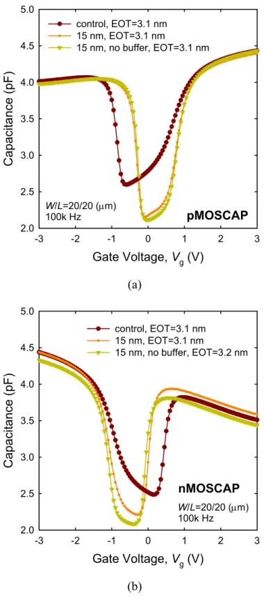
To investigate the effect of Si buffer under the SiGe epitaxy layer on the device characteristics, the 15 nm Si0.85Ge0.15 channel MOSFETs with and without 10 nm Si buffer
layer are fabricated. The capacitance-voltage (C–V) curves of pMOSFETs and nMOSFETs are illustrated in Fig. 4-1. The equivalent oxide thickness (EOT) of the N2O-annealed SiN
gate dielectric obtained by the accumulation capacitance is almost the same 3.1 nm for all devices. The difference between the accumulation and inversion capacitance is due to the poly depletion effect. In addition, the apparent shifts of flat band voltage (Vfb) for both the p- and
n- MOSCAPs with Si channel (control device) are caused by a higher substrate doping concentration than that of the SiGe channel devices.
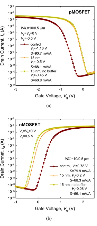
Figure 4-2 displays the Id–Vg characteristics of all samples. We can see that the Si buffer
layer does not affect the threshold voltages (Vt) and the subthreshold swings (S) because the Vt
and S have been shown to be almost the same for SiGe pMOSFETs and nMOSFETs. Again, the larger values of Vt and S for the control Si channel devices than that of the SiGe channel
excellent low values of subthreshold swings of around 67 mV/A for all SiGe MOSFETs reveal a good interface between the N2O-annealed SiN gate dielectric and the Si0.85Ge0.15
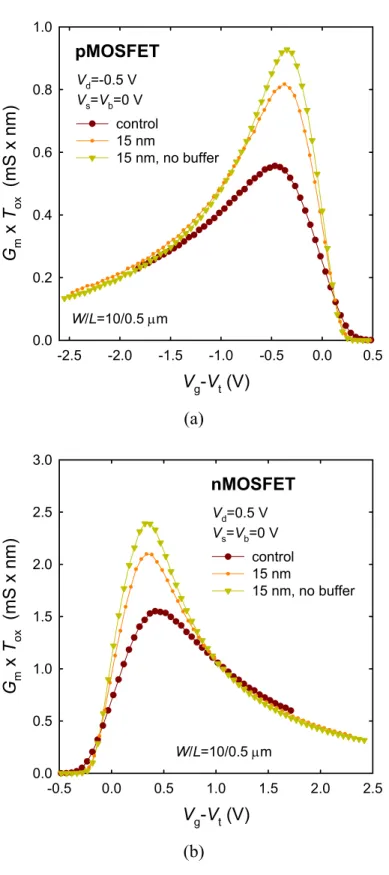
channel. Figure 4-3 shows the drain currents of the MOSFETs. Obviously, for both pMOSFETs and nMOSFETs, the SiGe devices show higher driving currents than that of the conventional Si devices, and the SiGe devices without Si buffer layer show slightly better performance than that of devices with a buffer layer. These results are corresponding to the trends of transconductance as shown in Fig. 4-4. For pMOSFETs and nMOSFETs, the peaks of the normalized transconductance (Gm×Tox) at the low Vg–Vt biases display the same results
as the Id–Vd curves in Fig. 4-3. The enhancement of Gm×Tox is probably due to the reduction
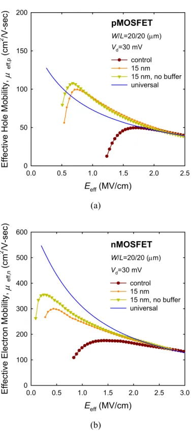
of interface states and carrier scattering effects. Additionally, the effective hole (µeff,p) and
electron (µeff,n) mobility for all MOSFETs are shown in Fig. 4-5. Although, the hole mobility
is improved by the compressive strain and quantum confinement in the Si0.85Ge0.15 channel for
pMOSFETs, the device without a buffer layer still shows higher µeff,p than that of the device
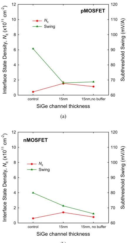
with a buffer layer. For nMOSFETs, the device without a buffer layer also shows superior effective electron mobility than that of the counterparts. Meanwhile, the improvement of the low field effective mobility for SiGe devices is mainly because of the decrease of the impurity scattering by their lower channel doping concentration. By measuring the charge pumping currents, the interface state density (Nit) can be extracted as plotted in the Fig. 4-6. We can see
that the values of Nit for all devices are almost the same for their good interface between the
Fig. 4-6 as comparing with the interface state density. As mentioned above, the values of swing for SiGe channel MOSFETs are lower than that for the conventional MOSFETs, and it is due to the lighter doping concentration in the SiGe channel.
Considering the same results of Vt, S, and Nit for the SiGe MOSFETs with and without Si
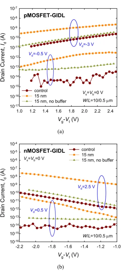
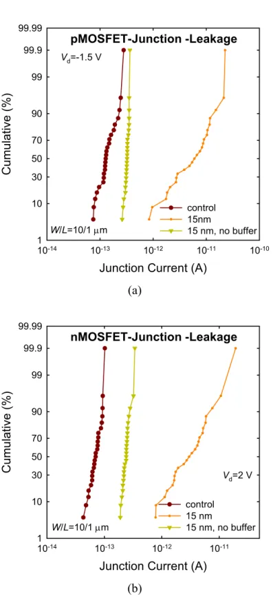
buffer layer, the enhancement of the driving current, transconductance, and the effective mobility for the device without a buffer layer should be contributed by other factors. Figure 4-7 demonstrates the characteristics of GIDL for p- and n- MOSFETs. Interestingly, we find that the leakage currents of SiGe devices with Si buffer layer are more than one order of magnitude larger than that of other devices for both pMOSFETs and nMOSFETs. Besides, junction leakage currents also show the same trends as the results of GIDL shown in Fig. 4-8. Therefore, we speculate that the increase of leakage current is caused by the excess dislocations in the SiGe channel because of the imperfect crystalline induced by the Si buffer layer. Then we believe that the SiGe channel MOSFETs will demonstrate superior device performance when the selective SiGe epitaxy layer is deposited directly on the Si substrate without a Si buffer layer to form the channel of device.
4-2 MOSFETs with 5, 15 and 30 nm SiGe Channel
The pMOSFETs and nMOSFETs with various SiGe channel thickness of 5, 15, and 30 nm without a Si buffer layer are fabricated to investigate the channel thickness effect on the
device characteristics. The gate dielectric is formed by the N2O-annealed LPCVD SiN. Figure
4-9 shows the C–V characteristics of the SiGe devices with different channel thickness. The smaller values of EOT (3.1 nm) are obtained for the devices with thinner SiGe channel of 5 and 15 nm. The 30 nm SiGe channel devices, however, have been shown to have larger EOT. It is speculated that the faster depositing rate of SiN layer is induced by the high surface strain energy of a thick SiGe channel. Again, the poly depletion effect is also observed in these C–V curves. In addition, the distortion of C–V curves of the devices with 30 nm SiGe channel indicates more interface states should exist in the oxide/SiGe interface, and a slightly Vfb shift
is probably due to a slightly heavier doping concentration in the channel.
Figure 4-10 and Fig. 4-11 show the characteristics of Id–Vg and Id–Vd, respectively. The
threshold voltages of the devices with thinner SiGe channel are lower than that of the 30 nm SiGe channel devices because of their smaller values of EOT and lighter channel doping concentration. Moreover, the lowest subthreshold swing of 67 mV/A can also be realized by the 5 and 15 nm SiGe channel devices, and it corresponds to the lower interface state density. The 5 and 15 nm SiGe channel devices performing better driving capability than that of the 30 nm counterparts are demonstrated as comparing their Id–Vd curves in Fig. 4-11. Then, all of
the interface state density (Nit) and the subthreshold swing for all devices are shown in Fig.
4-12. Obviously, for both pMOSFETs and nMOSFETs, the 30 nm SiGe channel devices having higher Nit and S are demonstrated. Furthermore, the higher dislocation density of the
junction leakage currents for pMOSFETs and nMOSFETs as shown in Fig 4-13 and Fig. 4-14, respectively. Both the currents of GIDL and junction leakage of the devices with 30 nm SiGe channel show more than one order of magnitude than that of the thinner channel thickness counterparts. The increase of the dislocation density is speculated to be caused by increasing the strain energy with the SiGe channel thickness. These results indicate that a poor interface and channel layer quality can be obtained when the thickness of SiGe channel is increased up to 30 nm.
The normalized transconductance (Gm×Tox) characteristics for p- and n- MOSFETs are
shown in Fig. 4-15. The Gm characteristics are almost identical for 5 and 15 nm SiGe channel
devices and they are higher than that of the MOSFETs with 30 nm channel thickness at the low gate biases because of the lower interface state and dislocation density. At high gate voltages, however, the transconductance of the 30 nm SiGe channel pMOSFET is enhanced because holes still flow through in the SiGe channel under high gate bias. But for the pMOSFETs with 5 and 15 nm SiGe channel, holes will mainly transport through the under Si channel when the larger gate voltages are applied. On the other hand, as shown in Fig. 4-15(b), the Gm of the nMOSFET with 30 nm SiGe channel is degraded in the whole field region
because of the insignificant improvement of the effective electron mobility in SiGe channel. The effective mobility of the SiGe MOSFETs with 5, 15 and 30 nm channel thickness is extracted in Fig. 4-16. Consequently, the effective hole mobility is improved by the compressive strain and the quantum confinement in the SiGe channel and shows the similar
trend of the channel thickness effect as the transconductance does, which is shown in Fig. 4-15. However, the effective electron mobility of the 30 nm channel nMOSFET is severely degraded because of the high density of interface state and dislocation as discussed previously.
Chapter 5
Conclusion
In this work, we have successfully fabricated MOSFETs with selectively epitaxial Si0.85Ge0.15 channel and ultra-thin (EOT=3.1 nm) N2O-annealed LPCVD SiN gate dielectric.
The offset of valence band between Si0.85Ge0.15 and Si substrate is about 0.1 eV from the
empirical equation. The conduction mechanism of gate current is fitted well by FN tunneling with an effective barrier height of 1.8 eV. The C–V curves showing insignificant variation on
Vfb and hysteresis when the capacitors being stressed under CVS and CCS up to 3000 seconds
indicate the good quality of the N2O-annealed SiN gate dielectric has been formed. On the
other hand, polarity dependent SILC has been observed and can be explained by anode hole injection (AHI) model. Subsequently, we have studied the effect of hot-carrier (HC) stressing and negative bias temperature instability (NBTI) on the SiGe channel pMOSFETs. From the power law of threshold voltage degradation versus the stress time, we have demonstrated that electron trapping dominates the degradation of device performance under the NBTI stressing, while interface state generation is predominant under the HC stressing conditions. However, the device stressed under NBTI at 100 ºC has been shown the lightest ∆Vt and ∆Gm because of
the self-recovery effect. In addition, electron trapping has been observed during the initial HC stressing under the condition of Vg=Vd. According to the results of charge pumping
measurement, the highest interface state density is generated after the device being stressed at
Vg=Vd and we have regarded the stressing condition of Vg=Vd as the worst case for evaluating
the reliability of the SiGe channel pMOSFET with N2O-annealed SiN gate dielectric.
The results of Vt, S, and Nit for the SiGe MOSFETs with and without the Si buffer layer
are indicated that the enhancement of the driving current, transconductance, and the effective mobility for the device without a buffer layer should be contributed by the lower dislocation density and higher carrier mobility than the counterparts. The dislocations in the SiGe channel, however, are due to the imperfect crystalline introduced in the Si buffer layer. Therefore, the SiGe MOSFETs have been demonstrated with superior device performance when the SiGe channel is deposited directly on the Si substrate without a Si buffer layer. Subsequently, we have also investigated the channel thickness effect on the SiGe pMOSFETs and nMOSFETs with various SiGe channel thickness of 5, 15, and 30 nm. The excellent subthreshold swings of 67 mV/A and high driving currents have been obtained for the MOSFETs with 5 and 15 nm SiGe channel. Moreover, the density of interface state and dislocation have been shown even lower than that of the 30 nm SiGe channel device. Although the 30 nm SiGe channel devices have been demonstrated having Gm and µeff degradation for both p- and n- MOSFETs
at low fields, higher effective hole mobility of pMOSFET is caused by holes still flowing through in the SiGe channel at high gate biases. Because the effective electron mobility can be improved insignificantly by the compressive strained SiGe channel, µeff,n of the 30 nm
whole voltage field. Finally, we have proposed the MOSFETs with thin SiGe channel (5 and 15 nm) and N2O-annealed SiN gate dielectric and shown their potential for advanced sub-100
References
[1] H.-S. P. Wong, “Beyond the conventional transistor,” IBM, VOL. 46, NO. 2/3, March/May 2002.
[2] ROOSEVELT PEOPLE, “Physics and Applications of GexSi1-x/Si trained-Layer
Heterostructures,” IEEE JOURNAL OF QUANTUM ELECTRONICS, VOL. QE-22, NO. 9, SEPTEMBER 1986.
[3] D. Wu, A.-C. Lindgren, S. Persson, G. Sjöblom, M. von Haartman, J. Seger, P.-E. Hellström, J. Olsson, H.-O. Blom, S.-L. Zhang, M. Östling, E. Vainonen-Ahlgren, W.-M. Li, E. Tois, and M. Tuominen, “A Novel Strained Si0.7Ge0.3 Surface-Channel pMOSFET
With an ALD TiN/Al2O3/HfAlOx/Al2O3 Gate Stack,” IEEE ELECTRON DEVICE
LETTERS, VOL. 24, NO. 3, MARCH 2003.
[4] Zhonghai Shi, David Onsongo, Katsunori Onishi, Jack C. Lee, and Sanjay K. Banerjee, “Mobility Enhancement in Surface Channel SiGe PMOSFETs With HfO2 Gate
Dielectrics,” IEEE ELECTRON DEVICE LETTERS, VOL. 24, NO. 1, JANUARY 2003. [5] T. Tezuka, N. Sugiyama, T. Mizuno and S. Takagi, “Novel fully-depleted
SiGe-on-insulator pMOSFETs with high-mobility SiGe surface channels,” IEDM
TECHNICAL DIGEST, 2001.
Strained-SiGe p-MOSFET with Enhanced Hole Mobility and Lower Parasitic Resistance,” VLSI Technology Digest of Technical Papers, 2002.
[7] Xiangdong Chen, Kou-Chen Liu, Qiqing Christine Ouyang, Sankaran Kartik Jayanarayanan, and Sanjay Kumar Banerjee, Fellow, IEEE, “Hole and Electron Mobility Enhancement in Strained SiGe Vertical MOSFETs,” IEEE TRANSACTIONS ON
ELECTRON DEVICES, VOL. 48, NO. 9, SEPTEMBER 2001.
[8] J. Alieu, T. Skotnicki, E. Josse, J.-L. Regolini and G. Bremond, “Multiple SiGe well: a new channel architecture for improving both NMOS and PMOS performances,” VLSI
Technology Digest of Technical Papers, 2000.
[9] Sang Kook Chun and Kang L. Wang, Fellow, IEEE, “Effective Mass and Mobility of Holes in Strained Si1-xGex Layers on (001) Si1-yGey Substrate,” IEEE TRANSACTIONS
ON ELECTRON DEVICES, VOL. 39, NO. 9, SEPTEMBER 1992.
[10] F. M. Bufler, P. Graf, B. Meinerzhagen, B. Adeline, M. M. Rieger, H. Kibbel, and G. Fischer, “Low- and High-Field Electron-Transport Parameters for Unstrained and Strained Si1-xGex,” IEEE ELECTRON DEVICE LETTERS, VOL. 18, NO. 6, JUNE 1997.
[11] W. Lu, X. W. Wang, R. Hammond, A. Kuliev, S. Koester, J. O. Chu, K. Ismail, Fellow,
IEEE, T. P. Ma, Fellow, IEEE, and I. Adesida, Fellow, IEEE, “p-Type SiGe Transistors
with Low Gate Leakage Using SiN Gate Dielectric,” IEEE ELECTRON DEVICE
LETTERS, VOL. 20, NO. 10, OCTOBER 1999.
“High Performance 0.15 mm Self-Aligned SiGe p-MOS-MODFET’s with SiN Gate Dielectric,” IEDM TECHNICAL DIGEST, 1999.
[13] S. Saito, Y. Shimamoto, S. Tsujikawa, H. Hamamura, O. Tonomura, D. Hisamoto, T. Mine, K. Torii, M. Hiratani, T. Onai, and S. Kimura, “Impact of Oxygen-enriched SiN Interface on Al2O3 Gate Stack An Innovative Solution to Low-power CMOS,” VLSI
Technology Digest of Technical Papers, 2003.
[14] Shimpei Tsujikawa, Toshiyuki Mine, Yasuhiro Shimamoto, Osamu Tonimura, Ryuta Tsuchiya, Kazuhiro Ohnishi, Hirotaka Hamamura, Kazuyoshi Torii, Takahiro Onai, and Jiro Yugami, “An Ultra-thin Silicon Nitride Gate Dielectric with Oxygen-enriched Interface (OI-SiN) for CMOS with EOT of 0.9 nm and Beyond,” VLSI Technology
Digest of Technical Papers, 2002.
[15] Ryuta Tsuchiya, Kazuhiro Ohnishi, Masatada Horiuchi, Shimpei Tsujikama, Yasuhiro Shimamoto, Naomi Inada, Jiro Yugami, Fumio Ootsuka, and Takahiro Onai, “Femto-Second CMOS Technology with High-k Offset Spacer and SiN Gate Dielectric with Oxygen-enriched Interface,” VLSI Technology Digest of Technical Papers, 2002. [16] C. Y. Chang, S. M. Sze, “ULSI Devices,” WILEY-INTERSCIENCE, New York, 2000. [17] S. Mahapatra, Chetan D. Parikh, V. Ramgopal Rao, Chand R. Viswanathan, Life Fellow,
IEEE, and Juzer Vasi, “Device Scaling Effects on Hot-Carrier Induced Interface and
Oxide-Trapped Charge Distributions in MOSFET’s,” IEEE TRANSACTIONS ON
[18] S. Mahapatra, Chetan D. Parikh, V. Ramgopal Rao, Chand R. Viswanathan, Life Fellow,
IEEE, and Juzer Vasi, “A Comprehensive Study of Hot-Carrier Induced Interface and
Oxide Trap Distributions in MOSFET’s Using a Novel Charge Pumping Technique,”
IEEE TRANSACTIONS ON ELECTRON DEVICES, VOL. 47, NO. 1, JANUARY 2000.
[19] Jone F. Chen, Chih-Pin Tsao, and T. -C. Ong, “Enhanced Hot-Carrier Induced Degradation in pMOSFETs Stressed Under High Gate Voltage,”
University/Government/Industry Microelectronics Symposium, 2003.
[20] G. Groeseneken, R. Bellens, G. Van den bosch and H. E. Maes, “TOPICAL REVIEW Hot-carrier degradation in submicrometre MOSFETs: from uniform injection towards the real operating conditions,” Semicond. Sci. Technol., 10, 1995.
[21] G. La Rosa, F. Guarin, S. Rauch, A. Acovic, J. Lukaitis, E. Crabbe, “NBTI-CHANNEL HOT CARRIER EFFECTS IN PMOSFETS IN ADVANCED CMOS TECHNOLOGIES,” Reliability Physics Symposium, 1997.
[22] Chul-Hee Jeon, Sam-Young Kim, Hyun-Soo Kim, Chae-Bog Rim, “The Impact of NBTI and HCI on Deep Sub-micron PMOSFETs’ Lifetime,” Integrated Reliability Workshop
Final Report, 21-24, Oct., 2002.
[23] Brian S. Doyle, Bruce J. Fishbein and Kaizad R. Mistry, “NBTI-Enhanced Hot Carrier Damage in p-Channel MOSFET’s,” IEDM TECHNICAL DIGEST, 1991.
[24] Shimpei Tsujikawa, Toshiyuki Mine, Kikuo Watanabe, Yasuhiro Shimamoto, Ryuta Tsuchiya, Kazuhiro Ohnishi, Takahiro Onai, Jiro Yugami, and Shinichiro Kimura,
“Negative Bias Temperature Instability of pMOSFETs with Ultra-thin SiON Gate Dielectrics,” IEEE 41st Annual International Reliability Physics Symposium, 2003.
[25] S. Mahapatra and M. A. Alam, “A Predictive Reliability Model for PMOS Bias Temperature Degradation,” IEDM TECHNICAL DIGEST, 2002.
[26] S. Mahapatra, P. Bharath Kumar and M. A. Alam, “A New Observation of Enhanced Bias Temperature Instability in Thin Gate Oxide p-MOSFETs,” IEDM TECHNICAL
DIGEST, 2003.
[27] Sanjay Rangan, Neal Mielke, Everett C.C. Yeh, “Universal Recovery Behavior of Negative Bias Temperature Instability,” IEDM TECHNICAL DIGEST, 2003.
[28] GREGORY J. DUNN and STEPHANIE A. SCOTT, “Channel Hot-Carrier Stressing of Reoxidized Nitrided Silicon Dioxide,” IEEE TRANSACTIONS ON ELECTRON
DEVICES, VOL. 37, NO. 7, JULY 1900.
[29] Muhammad A. Alam, Jeff Bude, and Andrea Ghetti, “Field Acceleration For Oxide Breakdown – Can An Accurate Anode Hole Injection Model Resolve the E vs. 1/E Controversy,” IEEE 38st Annual International Reliability Physics Symposium, 2000.
[30] Paul E. Nicollian, William R. Hunter, and Jerry C. Hu, “Experimental Evidence for Voltage Driven Breakdown Models in Ultrathin Gate Oxides,” IEEE 38st Annual
International Reliability Physics Symposium, 2000.
[31] P. Zaumseil and G. G. Fischer, “Comparison of the thermal stability of Si0.603Ge0.397/Si
[32] F. K. LeGoues, A. Powell, and S. S. Iyer, “Relaxation of SiGe thin films grown on Si/SiO2 substrates,” J. Appl. Phys., 75 (11), 1 June 1994.
ig. 2-1 Device process flow.
LOCOS Isolation
Selective UHVCVD Si
0.85Ge
0.15Channel Epitaxy (550ºC )
LPCVD SiN Deposition (780ºC)
+
RTA N
2O-annealing (800,900ºC, 30s)
LPCVD (620ºC) Poly-Si Gate Fabrication
Source/Drain Formation
RTA Dopant Activation (N
2, 900ºC, 30s)
Metallization
Si substrate
Gate
Si
0.85Ge
0.15channel
SiN + N
2O-annealing
Source
Drain
LOCOS
ig. 2-2 The structure of the Si0.85Ge0.15 channel MOSFETs.
x: the Ge content in the epi-layer
poly-Si
SiN
Si
1-x
Ge
x
Si-Sub
Hole Energy
Surface Channel
∆
E
v
~0.74x~0.1 |
x=0.15
(eV)
ig. 3-1 The band diagram of the Si0.85Ge0.15 channel device under the inversion condition.
Gate Voltage, Vg (V) -3 -2 -1 0 1 2 3 Capacit ance (pF) 3.0 3.2 3.4 3.6 3.8 4.0 4.2 4.4 4.6 inv-to-acc acc-to-inv W/L=20/20 (µm) , 100k Hz EOT=3.1 nm pMOSCAP (a) Gate Voltage, Vg (V) -4 -2 0 2 4 Gate Current Densit y, Jg ( A /c m 2 ) 10-9 10-8 10-7 10-6 10-5 pMOSCAP W/L=20/20 (µm) (b)
ig. 3-2 The electrical characteristics of the pMOSCAP with 50 nm Si0.85Ge0.15 channel and
F
N2O-annealed nitride gate dielectric. (a) The capacitance versus gate voltage. (b) The gate
1/
Ε
ox(MV/cm)
-10.080
0.085
0.090
0.095
0.100
ln(
J
g/
Ε
ox 2)
e
-22e
-21e
-20e
-19e
-18W/L=20/20 (µm)
pMOSCAP
φ
B=1.8 eV
FN tunneling
ig. 3-3 The fitting of the FN tunneling with an effective barrier height of 1.8 eV. F
Gate Voltage, Vg (V) -4 -2 0 2 4 Normalized Capacitance 0.3 0.4 0.5 0.6 0.7 0.8 0.9 1.0 initial 10s stress 110s stress 1100s stress 3000s stress 3000s stress @ Vg=-5.3 V 100x100 (µm2 ) , 100k Hz stress @ Vg=-5 V pMOSCAP inv-to-acc (a) Gate Voltage, Vg (V) -4 -2 0 2 4 Normalized Capacitance 0.3 0.4 0.5 0.6 0.7 0.8 0.9 1.0 inv-to-acc acc-to-inv 100x100 (µm2) , 100 kHz Vg=-5 V, stress 3000s pMOSCAP (b)
ig. 3-4 The normalized capacitances measured under constant voltage stress (CVS). (a) F
The characteristics of capacitance-voltage (C–V) with CVS time. (b) The hysteresis after –5 V stressing for 3000 seconds.
Gate Voltage, Vg (V) -2 -1 0 1 2 3 4 Normalized Capacitance 0.3 0.4 0.5 0.6 0.7 0.8 0.9 1.0 initial 10s stress 110s stress 1100s stress 3000s stress 3000s stress @ Jg=-0.02 mA/cm2 100x100 (µm2) , 100k Hz stress @ Jg=-0.01 mA/cm2 pMOSCAP inv-to-acc (a) Gate Voltage, Vg (V) -2 -1 0 1 2 3 4 Normalized Capacitance 0.3 0.4 0.5 0.6 0.7 0.8 0.9 1.0 inv-to-acc acc-to-inv 100x100 (µm2) , 100 kHz Jg=-0.01 mA/cm 2 , stress 3000s pMOSCAP (b)
Fig. 3-5 The normalized capacitances measured under constant current stress (CCS). (a) The
characteristics of capacitance-voltage (C–V) with CCS time. (b) The hysteresis after –5 V stressing for 3000 seconds.
Gate Voltage, Vg (V)
-4 -2 0 2 4
Gate Current Density,
J g (A/cm 2 ) 10-10 10-9 10-8 10-7 10-6 initial 10s stress 110s stress 1100s stress 3000s stress 3000s stress @ Vg=-5.3 V 100x100 (µm2) stress @ Vg=-5 V pMOSCAP stress time 10-5 (a) Gate Voltage, Vg (V) -4 -2 0 2 4 G a te Cu rrent Densi ty, Jg (A/cm 2 ) 10-10 10-9 10-8 10-7 10-6 initial 10s stress 110 stress 1100 stress 3000s stress 3000s stress @ Jg=-0.02 mA/cm2 100x100 (µm2) stress @ Jg=-0.01 mA/cm2 pMOSCAP stress time (b)
ig. 3-6 The characteristics of current-voltage (I–V) related to (a) CVS time and (b) CCS F
–
–
–
–
–
–
Gate Substrate
Oxide
Gate Voltage, Vg (V) -4 -3 -2 -1 0 Drain Current, I d (A ) 10-12 10-11 10-10 10-9 10-8 10-7 10-6 10-5 10-4 10-3 10-2 G m (m S) 0.00 0.02 0.04 0.06 0.08 0.10 0.12 Vd=-0.5 V Vd=-4 V Gm Vs=Vb=0 V W/L=10/0.5 µm Vt=-1.869 V S=124.8 mV/A pMOSFET (a) Drain Voltage, Vd (V) -4 -3 -2 -1 0 Dr ain Cu rrent , Id ( µA) 0 100 200 300 400 500 Vs=Vb=0 V Vg-Vt=0, -0.5, -1, -1.5, -2 V W/L=10/0.5 µm pMOSFET (b)
ig. 3-8 The electrical characteristics of Si0.85Ge0.15 channel pMOSFET with 50 nm
F
Si0.85Ge0.15 channel and N2O-annealed nitride gate dielectric. (a) The Id–Vg curves. (b) The
Stress Time (s) 101 102 103 104 ∆ Id /|Id | (%) -3.5 -3.0 -2.5 -2.0 -1.5 -1.0 -0.5 0.0 pMOSFET Vd=-4.5 V Vg=Vd Vg=2Vd/3 NBTI-RT NBTI-100oC (a) Stress Time (s) 101 102 103 104 ∆ G m /|G m | (%) -50 -40 -30 -20 -10 0 pMOSFET Vd=-4.5 V Vg=Vd Vg=2Vd/3 NBTI-RT NBTI-100oC (b)
ig. 3-9 The effects of HC and NBTI on pMOSFET with Si0.85Ge0.15 channel. (a) The Id
F
Stress Time (s)
10
210
310
4∆
V
t(V
)
0.001
0.01
0.1
1
pMOSFET
V
d=-4.5 V
∆
V
t=At
nV
g=V
d(n=0.33)
V
g=2V
d/3 (n=0.39)
NBTI-RT (n=0.13)
NBTI-100
oC (n=0.08)
ig. 3-10 The characteristics of threshold voltage shift versus stress time under different F
Vpeak (V) -4 -3 -2 -1 0 Charg e P u mpin g Current , I CP (nA ) -8 -6 -4 -2 0 post-Vg=Vd post-Vg=2Vd/3 post-NBTI-RT pre-Vg=Vd pre-Vg=2Vd/3 pre-NBTI-RT W/L=10/2 (µm), 1 MHz Vbase=0.5 V Vd=Vs=-0.1 V Vb=0 V pMOSFET Stress @ -5 V (a) Vpeak (V) -1.6 -1.5 -1.4 -1.3 -1.2 -1.1 -1.0 Charg e P u mpin g Current , I CP (nA ) -8 -6 -4 -2 0 post-Vg=Vd post-Vg=2Vd/3 post-NBTI-RT pre-Vg=Vd pre-Vg=2Vd/3 pre-NBTI-RT W/L=10/2 (µm), 1 MHz Vbase=0.5 V Vd=Vs=-0.1 V Vb=0 V pMOSFET (b)
ig. 3-11 (a) Compare of charge pumping current before and after stress. (b) Compare of F
Stress Conditions
Vg=Vd
Vg=2Vd/3
NBTI-RT
∆
N
it(x10
9cm
-2)
0
5
10
15
20
25
30
W/L=10/2 (µm), 1 MHz
V
d=V
s=-0.1 V
V
b=0 V
pMOSFET
ig. 3-12 The interface state densities generated by three stressing conditions at stressing F
1/|Vd| (V)-1 0.1 0.2 0.3 0.4 0.5 0.6 Lifetime @ ∆ Gm =-10% (s) 100 101 102 103 104 105 106 107 108 109 stress @ 104s pMOSFET Vg=Vd Vg=2Vd/3 (a) 1/|Vd| (V)-1 0.1 0.2 0.3 0.4 0.5 0.6 Li fe time @ ∆ Id =-1% ( s) 101 102 103 104 105 106 107 108 109 stress @ 104s pMOSFET Vg=Vd Vg=2Vd/3 (b)
ig. 3-13 The lifetime extracted from (a) Id degradation and (b) Gm degradation.
Stress Time (s) 101 102 103 104 ∆ I d /|I d | (%) -10 -8 -6 -4 -2 0 W/L=10/0.6 µm pMOSFET-HC Vg=Vd=-4.5 V Vg=Vd=-5 V Vg=Vd=-5.3 V (a) Stress Time (s) 101 102 103 104 ∆ G m /|G m | (%) -80 -60 -40 -20 0 W/L=10/0.6 µm pMOSFET-HC Vg=Vd=-4.5 V Vg=Vd=-5 V Vg=Vd=-5.3 V (b)
ig. 3-14 The stressing conditions of Vg=Vd. (a) The Id degradation and (b) the Gm
F
Stress Time (s)
10
110
210
310
4∆
V
t(V)
-0.15
-0.10
-0.05
0.00
0.05
0.10
0.15
pMOSFET-HC
W/L=10/0.6 µm
V
g=V
d=-4.5 V
V
g=V
d=-5 V
V
g=V
d=-5.3 V
ig. 3-15 The threshold voltage shifts by the stressing conditions of Vg=Vd.
Gate Voltage, Vg (V) -3 -2 -1 0 1 2 3 Capacit ance (pF) 2.0 2.5 3.0 3.5 4.0 4.5 5.0 control, EOT=3.1 nm 15 nm, EOT=3.1 nm 15 nm, no buffer, EOT=3.1 nm W/L=20/20 (µm) 100k Hz pMOSCAP (a) Gate Voltage, Vg (V) -3 -2 -1 0 1 2 3 Capacit ance (pF) 2.0 2.5 3.0 3.5 4.0 4.5 5.0 control, EOT=3.1 nm 15 nm, EOT=3.1 nm 15 nm, no buffer, EOT=3.2 nm W/L=20/20 (µm) 100k Hz nMOSCAP (b)
Fig. 4-1 The C–V characteristics of (a) pMOSCAPs and (b) nMOSCAPs with and without
the 10 nm Si buffer layer under Si0.85Ge0.15 channel. The control samples are the conventional
Gate Voltage, Vg (V) -3 -2 -1 0 Drain Cu rre nt, Id (A) 10-14 10-13 10-12 10-11 10-10 10-9 10-8 10-7 10-6 10-5 10-4 10-3 10-2 control Vt=-1.16 V S=90.7 mV/A 15 nm Vt=-0.5 V S=68.1 mV/A 15 nm, no buffer Vt=-0.45 V S=68.8 mV/A pMOSFET Vs=Vb=0 V Vd=-0.5 V W/L=10/0.5 µm (a) Gate Voltage, Vg (V) -1 0 1 2 Drain Cu rrn et, Id (A) 10-14 10-13 10-12 10-11 10-10 10-9 10-8 10-7 10-6 10-5 10-4 10-3 10-2 control, Vt=0.78 V S=79.9 mV/A 15 nm, Vt=0.2 V S=68.3 mV/A 15 nm, no buffer Vt=0.08 V S=66.1 mV/A nMOSFET Vs=Vb=0 V Vd=0.5 V W/L=10/0.5 µm (b)
Fig. 4-2 The Id–Vg characteristics of (a) pMOSFETs and (b) nMOSFETs with and without
the 10 nm Si buffer layer under Si0.85Ge0.15 channel. The subthreshold swings are small to
Drain Voltage, V
d(V)
-2.5 -2.0 -1.5 -1.0 -0.5 0.0 0.5 1.0 1.5 2.0 2.5
Drain Current,
I
d(mA)
0.0
0.5
1.0
1.5
2.0
2.5
3.0
Drain Current,
-I
d(mA)
0.0
0.5
1.0
1.5
2.0
2.5
3.0
V
s=V
b=0 V
V
g-V
t=2 V
W/L=10/0.5
µm
pMOSFET
control
15 nm
15 nm, no buffer
nMOSFET
V
g-V
t=-2 V
Fig. 4-3 The Id Vd haracteristics of pMOSFETs (left part) and nMOSFETs (right part) with 0.85 0.15
conventional Si channel devices.
– c
Vg-Vt (V) -2.5 -2.0 -1.5 -1.0 -0.5 0.0 0.5 G m x T ox (mS x nm) 0.0 0.2 0.4 0.6 0.8 1.0 control 15 nm 15 nm, no buffer Vd=-0.5 V Vs=Vb=0 V W/L=10/0.5 µm pMOSFET (a) Vg-Vt (V) -0.5 0.0 0.5 1.0 1.5 2.0 2.5 G m x T ox (mS x nm) 0.0 0.5 1.0 1.5 2.0 2.5 3.0 control 15 nm 15 nm, no buffer Vd=0.5 V Vs=Vb=0 V W/L=10/0.5 µm nMOSFET (b)
Fig. 4-4 The transconductance of (a) pMOSFETs and (b) nMOSFETs with and without the
channel devices.
Eeff (MV/cm) 0.0 0.5 1.0 1.5 2.0 2.5 Effective H ol e M obi lity, µeff,p (cm 2 /V-sec) 0 50 100 150 200 control 15 nm 15 nm, no buffer universal pMOSFET W/L=20/20 (µm) Vd=30 mV (a) Eeff (MV/cm) 0.0 0.5 1.0 1.5 2.0 2.5 3.0 E ffe ctive Elect ron Mobility, µeff,n (cm 2 /V-sec) 0 100 200 300 400 500 600 control 15 nm 15 nm, no buffer universal nMOSFET W/L=20/20 (µm) Vd=30 mV (b)
Fig. 4-5 (a) The effective hole mobility of pMOSFETs, and (b) the effective electron
SiGe channel thickness
control 15nm 15nm,no buffer
In terfa ce St at e D ens ity , N it (x 10 11 cm -2 ) 0 2 4 6 8 10 12 Sub thres hold Sw ing (mV/ A) 60 70 80 90 100 110 120 Nit Swing pMOSFET (a)
SiGe channel thickness
control 15nm 15nm, no buffer In terfa ce St at e D ens ity , N it (x 10 11 cm -2 ) 0 2 4 6 8 10 12 Sub thres hold Sw ing (mV/ A) 60 70 80 90 100 110 120 Nit Swing nMOSFET (b)
Fig. 4-6 The interface state density of (a) pMOSFETs and (b) nMOSFETs from charge
pumping technique. The relation between subthreshold swing and device structure has also een plotted.
Vg-Vt (V) 1.0 1.2 1.4 1.6 1.8 2.0 2.2 2.4 Drain Current, I d (A ) 10-17 10-16 10-15 10-14 10-13 10-12 10-11 10-10 10-9 10-8 10-7 control 15 nm 15 nm, no buffer Vs=Vb=0 V W/L=10/0.5 µm pMOSFET-GIDL Vd=-3 V Vd=-0.5 V (a) Vg-Vt (V) -2.2 -2.0 -1.8 -1.6 -1.4 -1.2 -1.0 Drain Current, I d (A ) 10-16 10-15 10-14 10-13 10-12 10-11 10-10 10-9 10-8 10-7 10-6 10-5 10-4 control 15 nm 15 nm, no buffer Vs=Vb=0 V W/L=10/0.5 µm nMOSFET-GIDL Vd=2.5 V Vd=0.5 V (b)
Fig. 4-7 The measured gate induced drain leakage (GIDL) of (a) pMOSFETs and (b)
nMOSFETs with and without the 10 nm Si buffer layer under Si0.85Ge0.15 channel. The control
Junction Current (A) 10-14 10-13 10-12 10-11 10-10 Cumulative (%) 1 10 30 50 70 90 99 99.9 99.99 control 15nm 15 nm, no buffer W/L=10/1 µm pMOSFET-Junction -Leakage Vd=-1.5 V (a)
Junction Current (A)
10-14 10-13 10-12 10-11 Cumulative (%) 1 10 30 50 70 90 99 99.9 99.99 control 15 nm 15 nm, no buffer W/L=10/1 µm nMOSFET-Junction -Leakage Vd=2 V (b)
Fig. 4-8 The junction leakage of (a) pMOSFETs and (b) nMOSFETs with and without the
Gate Voltage, Vg (V) -3 -2 -1 0 1 2 3 Capacit ance (pF) 2.0 2.5 3.0 3.5 4.0 4.5 5.0 5 nm, no buffer, EOT=3.1 nm 15 nm, no buffer, EOT=3.1 nm 30 nm, no buffer, EOT=3.5 nm W/L=20/20 (µm) 100k Hz pMOSCAP (a) Gate Voltage, Vg (V) -3 -2 -1 0 1 2 3 Capacit ance (pF) 2.0 2.5 3.0 3.5 4.0 4.5 5.0 5 nm, no buffer, EOT=3.1 nm 15 nm, no buffer, EOT=3.2 nm 30 nm, no buffer, EOT=3.4 nm W/L=20/20 (µm) 100k Hz nMOSCAP
Si buffer layer under the i0.85Ge0.15 channel.
(b)
Fig. 4-9 The C–V characteristics of (a) pMOSCAPs and (b) nMOSCAPs with different
SiGe channel thickness. All the MOSCAPs have no 10 nm S