國 立 交 通 大 學
電信工程學系
碩 士 論 文
具有快速頻率擷取之相位頻率偵測器與低抖動
之頻率合成器設計
Design of Low Jitter Frequency Synthesizers with Fast
Frequency Acquisition Phase-Frequency Detector
研 究 生:施宜興
指導教授:唐震寰 教授
具有快速頻率擷取之相位頻率偵測器與低抖動
之頻率合成器設計
Design of Low Jitter Frequency Synthesizers with Fast
Frequency Acquisition Phase-Frequency Detector
研 究 生:施宜興 Student:Yi-Shing Shih
指導教授:唐震寰 教授 Advisor:Jenn-Hwan Tarng
國 立 交 通 大 學
電 信 工 程 學 系 碩 士 班
碩 士 論 文
A ThesisSubmitted to Department of Communication Engineering College of Electrical Engineering and Computer Science
National Chiao Tung University in Partial Fulfillment of the Requirements
for the Degree of Master
in
Communication Engineering
July 2006
Hsinchu, Taiwan, Republic of China
具有快速頻率擷取之相位頻率偵測器與低抖動
之頻率合成器設計
研究生:施宜興 指導教授:唐震寰
國立交通大學
電信工程學系 碩士班
摘要
在現代無線通訊世界,鎖相迴路頻率合成器在射頻前端電路中扮演一個很重 要的角色。隨著無線通訊標準演進,鎖相迴路的設計涉及許多問題與折衷取捨, 如何達到低抖動、快速鎖定時間以及低消耗功率等的迫切要求,愈來愈具有挑戰 性。兩個關鍵重要的設計問題–死區(dead-zone)和盲區(blind-zone)均不利於鎖相 迴路的效能,分別會造成時序抖動及鎖定速度變慢。特別是,兩者無法同時兼顧, 縮減死區卻會增加盲區。 為克服這些問題,本篇論文的研究焦點著重於相位頻率偵測器的設計。找尋 且發展一個新的方法來消除死區和盲區。藉此,提出一個新型的相位頻率偵測 器。最後,結合我們所提出的相位頻率偵測器,我們利用台灣積體電路 0.18-μm CMOS 製程來實現一個操作在 2.36~2.95-GHz 的整數除頻頻率合成器。模擬結 果顯示,從 2.36 GHz 震盪頻率跳頻鎖定至 2.8 GHz 的情況下,本頻率合成器 在1.8伏特的電壓供應下所消耗的功率為 25.9mW,其鎖定時間為1.93μs,相較於 原始的頻率合成器改善了將近25%。Design of Low Jitter Frequency Synthesizer with Fast
Frequency Acquisition Phase-Frequency Detector
Student:Yi-Shing Shih Advisor:Dr. Jenn-Hwan Tarng
Department of Communication Engineering
National Chiao Tung University
Abstract
In the world of modern wireless communication, phase-locked loop (PLL) based frequency synthesizers have played an important role in RF front-ends. As the wireless standards evolve, it presents an increasing challenge to meet the stringent requirements of low jitter or phase noise, fast settling time, and low power in PLL designs, which involve a lot of design issues and trade-offs. Two crucial design issues, dead-zone and blind-zone are detrimental to the performance of PLLs, increasing the timing jitter and slowing the settling speed, respectively. In particular, the decrease of one of them may cause the increase of the other.
To overcome these issues, the research described in this thesis focuses on the design of phase-frequency detectors (PFDs). A new way to eliminate the dead-zone as well as the blind-zone has been founded and developed, whereby a novel and robust fast frequency-acquisition PFD is proposed. A 2.36~2.95-GHz integer-N frequency synthesizer including our proposed PFD is implemented in a standard TSMC 0.18-μm CMOS process. Simulation results reveal that the frequency synthesizer using our
proposed PFD shows a locking time of 1.93μs, which is an improvement of up to 25% over that using a conventional PFD, while consuming 25.9mW at a 1.8V supply in the case of starting at 2.36 GHz and locking at 2.8 GHz. In addition, as compared with other PFD architectures, our proposed PFD manifests itself as a robust design for higher operating frequency, and neither dead-zone nor blind-zone.
誌
謝
在碩士研究的這三年歲月,首先要感謝的是我的指導教授 唐震寰教授並致 上我最誠摯的謝意。感謝老師在專業的通訊領域中,給予我不斷的指導與鼓勵, 並賦予了實驗室豐富的研究資源與環境,使得這篇碩士論文能夠順利完成。 其次,要感謝波散射與傳播實驗室的學長們—鄭士杰學長、劉文舜學長、莊 博學長在研究上的幫助與意見,讓我獲益良多。感謝實驗室的同學—和穆、孟勳、 舜升等在課業及研究上的互相砥礪與切磋,以及生活上的多彩多姿。感謝學弟妹 們—逸倫、建傑、懷文、奕慶、豐吉、育正、志瑋、思云、蓓縝等,讓實驗室在 嚴肅的研究氣氛中增添了許多歡樂,有了你們,更加豐富了我這三年的研究生生 活。另外,也要感謝助理—梁麗君小姐,在生活上的協助和籌劃每次的美食聚餐 饗宴。 最後,要感謝的就是我最親愛的家人,由於他們在我求學過程中,一路陪伴 著我,給予我最溫馨的關懷與鼓勵,讓我在人生的過程裡得到快樂,更讓我可以 專心於研究工作中而毫無後顧之憂。 鑒此,僅以此篇論文獻給所有關心我的每一個人。 施宜興 誌予 九十五年七月Table of Contents
中文摘要……….……….. I Abstract………II 誌謝………..IV Table of Contents……….V List of Tables………...……….VIII List of Figures……….IXCHAPTER 1
Introduction
.………...1
1.1 Background and Problems.………..1
1.2 Related Works………...5
1.2.1 Review on Phase-Frequency Detectors………..5
1.2.2 Review on Dual-Modulus Prescalers....………..8
1.3 Motivation……….9
1.4 Thesis Organization.………...………10
CHAPTER 2
Basics of Frequency Synthesizers
.………..12
2.1 General Considerations.……….13
2.1.1 Tuning Range………....13
2.1.2 Phase Noise………...13
2.1.3 Spurs……….15
2.1.4 Settling Time……….17
2.2 Frequency Synthesizer Architectures.………...17
2.2.1 Integer-N Architecture………..17
2.2.2 Fractional-N Architecture……….19
2.3 Fundamentals of Phase Locked Loop (PLL)………...22
2.3.1 Phase Frequency Detector (PFD)……….………22
2.3.2 Charge Pump (CP)………24
2.3.3 Loop Filter (LF)………25
2.3.4 Voltage-Controlled Oscillator (VCO)………...26
2.4 Modeling and Analysis of Frequency Synthesizer.………..31
2.4.1 Loop Stability Analysis………31
2.4.2 Static Phase Error Analysis……….….38
2.4.3 Phase Noise Performance Analysis………..41
CHAPTER 3
Fast Frequency Acquisition Phase/Frequency
Detectors (PFD) Design
..……….45
3.1 Introduction……….…………..………...45
3.2 Conventional tri-state PFD Architecture.…...……….……47
3.3 Proposed PFD Architecture………...49
3.4 Circuit Design and Simulation………..54
3.5 Conclusion………...56
CHAPTER 4
High Speed Dual-Modulus Prescalers Design
.……..57
4.1 Introduction.………57
4.2 Circuit Topology and Principle of Operation.………..58
4.3 Simulation Results………..62 4.4 Conclusion………...64
C
C
H
H
A
A
P
P
T
T
E
E
R
R
5
5
F
F
r
r
e
e
q
q
u
u
e
e
n
n
c
c
y
y
S
S
y
y
n
n
t
t
h
h
e
e
s
s
i
i
z
z
e
e
r
r
C
C
i
i
r
r
c
c
u
u
i
i
t
t
D
D
e
e
s
s
i
i
g
g
n
n
a
a
n
n
d
d
S
S
i
i
m
m
u
u
l
l
a
a
t
t
i
i
o
o
n
n
…
…
…
…
…
…
…
…
…
…
…
…
…
…
…
…
…
…
…
…
…
…
…
…
…
…
…
…
…
…
…
…
…
…
6
6
5
5
5.1 Introduction………655.2 Voltage-Controlled Oscillator Design.………...66
5.2.1 Phase Noise Theory…..………67
5.2.2 Circuit Topology and Design………71
5.2.3 Simulation Results………74
5.3 Frequency Divider Design……….75
5.3.1 Pulse-Swallow Frequency Divider………...75
5.3.2 Simulation Results.………...77
5.4 Phase-Frequency Detector Design………78
5.5 Charge Pump and Loop Filter Design.……….80
5.5.1 Charge Pump Circuit Topology………81
5.5.2 Loop Filter………82
5.5.3 Simulation Results………84
CHAPTER 6
Conclusion and Future Works……….…………..…90
6.1 Conclusion…..……….…90 6.2 Future Works………..91
List of Tables
Table 2.1 Relationship between γ and PM………...……….…37
Table 2.2 Static phase error for various types of PLLs………...……….40 Table 3.1 Typical delay values of a 0.18-μm CMOS technology……….54 Table 3.2 Comparison of the proposed PFD with recently-published related
literature………....55 Table 4.1 State tables: (a) dvide-by-4 counter (b) dvide-by-3 counter………....59 Table 4.2 Comparison between Rana’s and proposed DMP………64 Table 5.1 (a) The pulse-swallow divider step function (100 MHz fref)…………76
(b) The pulse-swallow divider step function (200 MHz fref)…...…….77
Table 5.2 The final PLL parameters in this work……….84 Table 5.3 Summary of the simulation results of frequency synthesizer…….…..89
List of Figures
Figure 1.1 Block diagram of a generic transceiver architecture……….…..2
Figure 1.2 PLL jitter introduced by the PFD dead zone………..3
Figure 1.3 The PFD blind zone and its phase characteristic………4
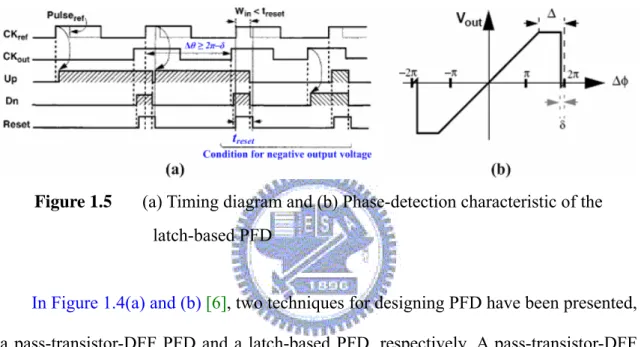
Figure 1.4 Circuit schematics [6] (a) a pass-transistor DFF PFD (b) a latch-based PFD……….5
Figure 1.5 (a) Timing diagram (b) Phase-detection characteristic of the latch -based PFD……….6
Figure 1.6 A novel precharged PFD [7].…………...………...7
Figure 1.7 (a) The proposed PFD architecture [8] (b) Its phase-detection characteristic……….………..8
Figure 2.1 Block diagram of a PLL-based frequency synthesizer……….12
Figure 2.2 (a) Ideal (b) Actual output spectrum of an oscillator...……….14
Figure 2.3 Effect of phase noise in (a) the receive path (b) the transmit path…...14
Figure 2.4 (a) Spurs (b) Effect of spurs in the receive path………15
Figure 2.5 Reference frequency feed-through.………...16
Figure 2.6 A simple charge pump PLL-based frequency synthesizer…………....18
Figure 2.7 A full divider with a dual-modulus prescaler and two counters……...19
Figure 2.8 A fractional-N frequency synthesizer with an accumulator…………..20
Figure 2.9 Classical phase interpolation method for spur cancellation………….21
Figure 2.10 Characteristic of an ideal phase detector...………...22
Figure 2.11 PFD characteristic………...23
Figure 2.12 Conceptual operation of a PFD.………23
Figure 2.13 State diagram of a three-state PFD………24
Figure 2.14 Block diagram of PFD with CP and the timing diagram...…………..25
Figure 2.16 VCO characteristic………...26
Figure 2.17 Illustration of phase variation of VCO with a voltage step ΔV………27
Figure 2.18 Different types of prescaler: (a) fixed modulus (b) dual modulus…...29
Figure 2.19 Timing diagram of the pulse-swallow frequency divider………...30
Figure 2.20 Linear model of a generic PLL....………...31
Figure 2.21 (a) Linear model of a 2nd order CPPLL (b) Its open-loop Bode plot....33
Figure 2.22 (a) Linear model of a compensated 2nd order CPPLL (b) Its open-loop Bode plot………..34
Figure 2.23 Granular transient response of a PLL with first-order loop filter…….35
Figure 2.24 Linear model of a type-II 3rd order CPPLL………..36
Figure 2.25 Open-loop Bode plot of type-II 3rd CPPLL………..36
Figure 2.26 The interrelation between each pole and zero………...……37
Figure 2.27 Linear model of the type-II 3rd CPPLL with noise sources…………..41
Figure 2.28 PLL noise transfer functions (a) from VCO (b) from Ref. noise…….43
Figure 2.29 Phase noise contributions in a PLL (a) VCO output phase noise (b) Ref. output phase noise (c) PLL output phase noise (before and after optimizing the loop bandwidth, respectively………....44
Figure 3.1 A conventional tri-state PFD and its state diagram………..47
Figure 3.2 Timing diagram of a tri-state PFD, presenting its non-ideal behavior.48 Figure 3.3 Phase characteristic of the ideal / non-ideal PFD……….49
Figure 3.4 Proposed tri-state PFD architecture………..50
Figure 3.5 Timing diagram of the proposed tri-state PFD……….51
Figure 3.6 Phase-discriminator characteristic of the proposed PFD……….51
Figure 3.7 Frequency characteristics of the proposed and conventional PFDs….53 Figure 3.8 Implementation of logic flip-flops in our proposed PFD……….54
Figure 3.9 Simulated frequency acquisition for the proposed and conventional PFDs……….55
Figure 4.1 Circuit schematics: (a) TG-based divide-by-3/4 counter (b) NOR-based divide-by-3/4 counter……….58
Figure 4.2 Proposed divide-by-3/4 dual-modulus prescaler………..59
Figure 4.3 Block diagram of the divide-by-127/128 DMP………61
Figure 4.4 Waveforms of the divide-by-127/-128 outputs at 5 GHz……….62
Figure 4.5 Simulated maximum operating frequency and power consumption of DMPs versus power supply voltage……….63
Figure 5.1 The architecture of integer-N frequency synthesizer in this thesis…..65
Figure 5.2 Leeson’s phase noise model……….67
Figure 5.3 Basic model of the oscillator circuit……….68
Figure 5.4 Two typical LC-tank oscillator structures: (a) complementary cross-coupled VCO (b) All-NMOS cross-coupled VCO……….71
Figure 5.5 Phase noise for the complementary and NMOS only………..72
Figure 5.6 Complementary cross-coupled LC VCO without the tail current source………73
Figure 5.7 Simulated phase noise of the LC VCO……….74
Figure 5.8 Simulated output frequency tuning of VCO……….74
Figure 5.9 Block diagram of the pulse-swallow frequency divider………...75
Figure 5.10 Generic architecture of the programming and swallow counters…..76
Figure 5.11 Pulse-swallow frequency divider with our proposed divide-by-3/4 DMP………...77
Figure 5.12 Simulated waveforms of the divide-by-3/4 DMP………77
Figure 5.13 Simulation results of the programming and swallow counters (÷13/14)………78
Figure 5.14 Circuit schematic of the classical dead-zone-free precharged PFD….79 Figure 5.15 (a) Both inputs have equal frequency but R leads V (b) R has a higher frequency than V (c) Comparison of the proposed (Upper diagram) and conventional (Down diagram) PFD at large phase errors.………80
Figure 5.16 Circuit schematics: (a) positive-feedback charge pump (b) charge pump in [27]...………..81
Figure 5.17 PLL loop filter design software………83 Figure 5.18 Bode plot of the loop gain and phase margin in this frequency
synthesizer design……….83 Figure 5.19 Simulation results of the charge pump (a) charging (b) discharging…84 Figure 5.20 Behavior model by Simulink………85 Figure 5.21 Simulated locking time from 2.36 to 2.6 GHz by Simulink……....….86 Figure 5.22 Simulated locking time from 2.36 to 2.8 GHz by Simulink…....…….86 Figure 5.23 (a) Simulated locking time from 2.36 to 2.6 GHz by ADS
(b) Its stable output spectrum at 2.6 GHz……….87 Figure 5.24 (a) Simulated locking time from 2.36 to 2.8 GHz by ADS
CHAPTER 1
Introduction
1.1 Background and Problems
Over the past few years, the wireless communications industry has experienced rapid and incredible growth, much of which has been driven by the rapidly-growing wireless market such as mobile telecommunications. But not only has the market for mobile telecomm grown; during the last couple of years, all kinds of previously wired connections between home and office appliances have been going wireless as well. The cellular phone has a calendar function that synchronizes automatically with the desktop calendar through a Bluetooth connection; the laptop computer accesses the Internet for multimedia services through a WLAN or emerging WiMAX connection, etc. So, there introduces a growing demand for wireless communication in today’s world.
In wireless communication systems, low cost, low power consumption, and high performance are the critical requirements due to the highly competitive market environment and limitation in battery life. In order to meet a growing demand for wireless communication, it’s desirable to implement radio transceivers monolithically with the help of improving large-scale low-cost integration technology. At present, GaAs, silicon bipolar, and BiCMOS technologies constitute a major section of the RF transceivers market because these technologies provide useful features such as high breakdown voltage and high cutoff frequency, etc. However, they are still expensive and low-density integration technologies so as not to satisfy people’s desire for low cost, small size, high portability, and good performance. Fortunately, as the deep-submicron
CMOS process evolves, CMOS technology has strong advantages of low cost and high density compared to other available technologies. Moreover, CMOS technology has the high potential to achieve a fully-integrated solution for system-on-a-chip (SOC), which realizes the addition of back-end digital function with the RF front-end circuit. So, in order to achieve the ultimate goal of SOC, many efforts have devoted to well design and implement a transceiver in CMOS process, as well as increase the integration level.
In the world of modern wireless communication, phase-locked loop (PLL) based frequency synthesizers have played an important role in RF front-ends. PLL-based frequency synthesizers are used to provide clean, stable, and precise carrier signals for frequency translation in wireless transceivers, as shown in Figure 1.1 which illustrates a generic transceiver architecture. As the wireless standards evolve, it presents an increasing challenge to meet the stringent requirements of low jitter or phase noise, fast settling time, and low power in PLL-based frequency synthesizer designs, which involve a lot of design issues and trade-offs.
The important system performance specifications for a frequency synthesizer are timing jitter, locking time, spectral purity, power dissipation, and manufacturing cost, etc. Within different PLL-based topologies, a popular low-cost architecture is the charge-pump PLL-based (CPPLL-based) frequency synthesizers, in which an ideal phase-frequency detector (PFD) is incorporated with an ideal charge pump (CP) to provide an infinite dc gain with passive filters, resulting in an unbounded pull-in range and zero static phase error [1]. However, in reality there exist many non-idealities in both PFD and CP or PFD/CP combination, such as dead zone, blind zone, current mismatch/leakage, charge sharing/injection, etc. These non-idealities are all detrimental to the overall performance of frequency synthesizers and should be avoid or alleviated. Here, the following brief description of how these non-idealities influence the system will give us a preliminary insight into the problems and trade-offs in CPPLL designs.
First, in a CPPLL, one of the critical building blocks is the tri-state PFD due to its frequency-detection capability. A conventional tri-state PFD suffers from the “dead zone” problem, which occurs when the loop is in a lock mode and the output of the following CP don’t change for small phase changes in the input signals at PFD. Any phase error within the dead-zone will disturb the VCO control voltage and directly translate to phase jitter in the PLL output, as shown in Figure 1.2.
Second, in order to eliminate the dead-zone, an added delay is inserted in the reset path to maintain a minimum pulse width when the two input signals are in phase. However, such a solution presents a limit on its maximum operating frequency and introduces another problem called “blind zone”, where any input transition will be overridden for large phase errors. Any input transition override results in the wrong output polarity (Figure 1.3) and longer frequency acquisition time.
Figure 1.3 The PFD blind zoneand its phase characteristic
Third, in addition to the above-mentioned issues, one of the other design issues is the unwanted FM modulation, which causes the reference spurs. Any non-idealities in the PLL itself causes periodic ripples on the VCO control line, which will in turn result in undesired spurs at the upper and lower sideband of the carrier. The dominant spurious-generating block in the PLL is the charge pump, the non-idealities of which mainly are: 1) the mismatch between the CP current sources (both random and due to channel-length modulation); 2) the mismatch between the charge injection and clock feedthrough of the pMOS and nMOS switches in the CP; 3) the mismatch between the arrival times of the input control pulses; 4) the mismatch of the widths of the input control pulses. Charge sharing also exacerbates the ripples [2].
1.2 Related Works
Over the past few years, a large amount of literature has been contributed to the study of how to solve these issues and improve the PLL performance. However, there is still a lot of work to be done in the field. In view of this, the focus of our work is on finding better ways to alleviate or even completely ameliorate these issues but except the FM-modulation issue. The following subsections comes the overview of the related works referred in our thesis.
1.2.1
Review on Phase-Frequency Detectors
Figure 1.4 Circuit schematics [6] (a) a pass-transistor DFF PFD, and (b) a
latch-based PFD
As stated in the previous section, a conventional tri-state PFD suffers from the dead-zone issue which worsens the PLL output jitter. Roughly, there are two ways to alleviate this problem. One way is to reduce the intrinsic reset time [3], [4], thus shortening the dead-zone. This in turn alleviates the speed and jitter limitations. Nevertheless, such a method offers only limited improvement on the issue. The other way is to add an additional delay in the reset path for enough pulse width to drive the
following stage [1], [3]. This would be a relatively simple and effective method, which could completely eliminate the dead-zone. Unfortunately, such a way introduces the blind-zone (Figure 1.3). It’s obvious that the blind zone is detrimental to the PLL settling behavior, and will slow down the locking time. In view of this, some extensive studies have been undertaken recently and expected to address both issues together
[5]-[8].
Figure 1.5 (a) Timing diagram and (b) Phase-detection characteristic of the
latch-based PFD
In Figure 1.4(a) and (b)[6], two techniques for designing PFD have been presented, a pass-transistor-DFF PFD and a latch-based PFD, respectively. A pass-transistor-DFF PFD shows a smaller reset delay, only including one pass-transistor, one inverter, and one NAND gate. As a result, a reduced blind-zone and faster frequency acquisition can be achieved. In Figure 1.4(b), by using pulse latches instead of flip-flops, the latch-based PFD fundamentally changes the dependence on the reset delay. This is illustrated in the timing diagram of Figure 1.5(a).When CKref arrives during the Reset ,
the edge information propagates to the output as long as CKref is still high
(level-sensitive) when the blind-zone duration ends. The PFD no longer loses the edge that arrives during the Reset and doesn’t output wrong polarity. The phase-detection characteristic is shown in Figure 1.5(b). It should note that the input pulse widths should be designed to be slightly smaller than the reset pulse width so that an input that triggers
the Reset would not assert the output after the Reset pulse ends; otherwise, the PFD will fail to lock at zero phase error. This design criterion results in wrong output polarity for Δθ ≥ 2π–δ. Thus, there still exhibits a very small blind-zone, whereas its operating frequency potentially approaches twice that of either the first proposed PFD or the conventional PFD for the same Reset time.
Figure 1.6 A novel precharged PFD in [7]
Figure 1.6[7] also shows a novel precharged PFD, which employs the same idea as in [6]. Noninverting delay stages are inserted into the commonly used precharged PFD so that it generates effective control signals even when the phase error approaches 2π. The novel precharged PFD has the same phase-detection characteristic but lower power consumption and higher precision as compared to the latch-based PFD [6]. Similarly, it also has a very small blind-zone, and the maximum operating frequency is dependent on the duty ratio of each input clock. Assume 50% duty ratio, the maximum operating frequency is half that of [6].
rely on any assumption on the underlying VLSI technology. The proposed PFD is divided two parts: one is the classical tri-state PFD using flip-flops with asynchronous set and reset inputs, and the other is the FZ-detector, which takes over the detection process once inside the blind-zone. The proposed PFD forces a set signal when an input transition occurs inside the blind-zone, thereby avoiding setting the wrong output and enhancing the frequency acquisition capabilities. Compared with the conventional PFD, its operating frequency shows an improvement of about 36%. Figure 1.7(b) shows the corresponding phase-detection characteristic.
(a) (b)
Figure 1.7 (a) The proposed PFD architecture [8]; (b) Its phase-detection
characteristic
1.2.2
Review on Dual-Modulus Prescalers
A high-frequency CMOS PLL frequency synthesizer has stringent requirements on dual-modulus prescaler (DMP). High speed, high moduli, and low power dissipation are the challenges in DMP designs. Typically, a DMP usually comprises of a synchronous dual-modulus counter, followed by an asynchronous counter. The critical path delay and the speed of the DFFs in the synchronous counter limit its overall speed, particularly at high divide-by-value. High divide-by-value is, in general, achieved by adding flip-flops
in the asynchronous counter at the cost of additional loading to the synchronous counter which results in degraded performance. Therefore, there is a trade-off between the speed and the divide-by-value.
Conventionally, most high-moduli DMPs usually comprise of a synchronous divide-by-4/5 counter, followed by a chain of toggle flip-flops, which forms an asynchronous counter. The operating speed of DMPs is mainly limited by that of the divide-by-4/5 counter. Unlike the conventional divide-by-4/5 counter [9], a novel topology for a divide-by-3/4 counter using transmission gates (TGs) in the critical path for mode selection is proposed by R. S. Rana [10]. The author has demonstrated that the TG-based divide-by-3/4 counter provides higher speed compared to the conventional divide-by-4/5 counter. However, an alternative divide-by-3/4 counter using NOR gates in the critical path is also presented and taken into account for further comparison by R. S. Rana [10]. With the help of Hspice simulation, the results show that the NOR-based divide-by-3/4 counter provides higher speed than the TG-based one due to smaller feedback path delay even though the critical path delay is more. For enhancing the speed of the TG-based divide-by-3/4 counter further, the author expects to shorten the D flip-flop (DFF) delay for future improvement.
1.3 Motivation
Nowadays, modern wireless system applications have an increasing demand to fabricate low-cost high-performance RF integrated circuits. In the world of wireless communications, frequency synthesizer is one of the critical components for RF front-end transceivers. As the demands for high-performance RF front-end transceivers grow rapidly, designing high-performance PLL-based frequency synthesizers becomes challenging. In general, the challenging design requirements of a frequency synthesizer
are low jitter or phase noise, fast settling time, and low power etc.
How to design a high-frequency, fast-settling, and low-jitter synthesizer? We start this thesis with a thorough insight into the dead-zone and blind-zone problems. We then survey the recently-published related literature. Afterward, we try to find new ways of eliminating these problems and further achieving a low-jitter and faster-locking frequency synthesizer. For high-frequency applications, the need for a high-speed and high-moduli dual modulus prescaler (DMP) also introduces stringent requirements due to its limitation on the operating speed of the frequency synthesizer. So, we also make some efforts to develop a high speed DMP in this work.
Therefore, this thesis focuses on the design of the new architecture of PFD, which incorporates an auxiliary circuitry to enhance the frequency acquisition capabilities. The novel proposed architecture suffers no problem of dead zone and blind zone, and has much better phase- and frequency-detection characteristics. It is implemented in a 2.36~ 2.95-GHz CMOS frequency synthesizer, including an improved high-speed divide- by-3/4 dual-modulus prescaler.
1.4 Thesis Organization
To achieve a low-jitter and fast-locking frequency synthesizer, this thesis presents a new fast frequency acquisition PFD with better phase- and frequency-discriminator characteristics. It also presents a new dual-modulus prescaler for high speed operation. This thesis is organized into the following chapters. Chapter 2 will give some general design considerations of PLL-based frequency synthesizer as well as basic behavior characteristics of its individual building blocks. A comprehensive and in-depth analysis of the noise behavior and loop stability of frequency synthesizers provides an insight into the design issues and trade-offs. Chapter 3 introduces a novel fast frequency
acquisition PFD with a detailed analysis of its phase- and frequency-discriminator characteristics. With the help of HSPICE and ADS simulation, the results demonstrate its robustness in PLL designs. Chapter 4 introduces a modified high-speed divide-by-3/4 dual-modulus prescaler and provides some simulation results to prove its improvement over the original one published by Rana [10]. Chapter 5 presents the circuit design and implementation of the building blocks of the frequency synthesizer, including voltage-controlled oscillator (VCO), frequency divider, PFD, charge pump and loop filter. Chapter 6 concludes this thesis with a summary and future work.
CHAPTER 2
Basics of Frequency Synthesizers
In a typical RF front-end circuit, the local oscillator is usually embedded in a phase-locked loop (PLL) as a tunable frequency synthesizer to provide clean, stable and more precise carrier signals for frequency up/down-conversion. The frequency synthesizer needs to be tunable in order to address all frequency channels and be fast switching to perform the addressing sufficiently fast. A basic block diagram of a PLL-based frequency synthesizer is shown in Figure 2.1. The loop provides a feedback to keep the output frequency of the synchronized oscillator to be a multiple of the reference frequency, i.e. fout=M· fref, where fout is the output frequency and fref is the
reference frequency.
This chapter begins with the general design considerations of a PLL-based frequency synthesizer, following which comes the overview of two widely-used frequency synthesizer architectures. Subsequently, the behavior characteristics of individual functional blocks (in Figure 2.1) are described and discussed. In conclusion, the noise behavior and loop stability of a frequency synthesizer are analyzed then to draw some conclusions of design issues and trade-offs.
2.1 General Considerations
The most important design considerations of a frequency synthesizer are tuning range, phase noise, spurs, and settling time. Their impacts on general wireless communication systems are investigated in this chapter.
2.1.1 Tuning
Range
The basic requirement set for a frequency synthesizer by any wireless communication system is that the synthesizer must be able to generate all required frequencies of the system with a sufficient accuracy for channel selection. Therefore, the voltage-controlled oscillator (VCO) and the prescaler must be carefully designed so as to cover the required dynamic frequency range of the synthesizer.
2.1.2 Phase
Noise
A spectral purity of synthesized output signal is the most important requirement in all wireless communication systems. Ideally, the output spectrum of a frequency synthesizer should be a pure tone at the desired frequency, as shown in Figure 2.2(a). In the time domain, the output can be expressed by Eq. (2.1).
0
( ) cos( )
out
v t = ⋅A ω t (2.1) However, due to random amplitude and phase fluctuations, the actual output becomes
[
]
[
]
( ) ( ) cos 0 ( )
out t
v = A+ε t ⋅ ω t+ t (2.2) θ , where ε( )t represents amplitude fluctuations and θ( )t represents phase fluctuations. The actual output spectrum exhibits “skirts” around the desired carrier impulse in the frequency domain, as shown in Figure 2.2(b). Because the amplitude fluctuations can be removed or greatly reduced by a limiter, the phase fluctuations, expressed in terms of phase noise, become a bigger and dominant concern in frequency synthesizer design. The phase fluctuations could be attributed to either the external noise at the frequency-
(a) (b)
Figure 2.2 (a) Ideal; (b) Actual output spectrum of an oscillator.
tuning input of the oscillator or the noise sources such as thermal, shot, or flicker noise of the devices in the oscillator.
The phase noise limits the quality of the synthesized signal. In order to quantify the phase noise, the total noise power within a unit bandwidth at an offset frequency (Δω) from the carrier frequency (ω0) is compared with the carrier power. As shown in Figure 2.2(b), this quantity is defined as Eq. (2.3) in the unit of dBC / Hz.
{ }
10 log sideband( 0 ,1 carrier P L P ω ω ω ⎡ + Δ Hz)⎤ Δ = ⋅ ⎢ ⎥ ⎣ ⎦ (2.3), where Psideband(ω0+ Δω,1Hz) represents the single sideband noise power within a 1Hz bandwidth at an offset frequency (Δω).
(a) (b)
Figure 2.3 illustrates the impact of the oscillator or synthesizer phase noise in both the receive path and transmit path of a transceiver. As depicted in Figure 2.3 (a), in the receive path, the weak desired signal is accompanied by a larger interferer in the adjacent channel. Ideally, the received RF signal is down-converted with a pure LO signal into the desired pure IF signal and the down-converted interferer can be easily filtered. However, in reality, there exists a phase noise skirt around the LO signal. After down-conversion, the weak desired signal could be corrupted by the tail of the interferer spectra and even possibly swamped out if the phase noise skirt is too large. This effect is called “reciprocal mixing”, and it degrades the SNR of the desired signal. In the transmit path, the weak nearby signal of interest can be corrupted by the tail of the large-power transmitted signal, as shown in Figure 2.3 (b).
Therefore, the output spectrum of the LO or synthesizer must be extremely sharp, and a set of stringent phase noise requirements must be achieved so as to satisfy the maximum blocking signal power specified in the wireless communication system.
2.1.3 Spurs
Apart from the phase noise, the other key parameter affecting the spectral purity of synthesized output signal is the relatively high-energy spurious tones (also called spurs), appearing as spikes above the noise skirt, as shown in Figure 2.4 (a).
Any systematic disturbance on the tuning input of the oscillator will cause the periodic phase variation and thus modulate the synthesized output. In the frequency domain, it manifests itself as the undesired tones at the upper and lower sideband of the carrier. These tones can be quantified by the difference between the carrier power and the spurious power at certain frequency offset in the dBC unit. The most common type
of spur is the reference spur that appears at multiples of the comparison frequency. Due to the non-ideal switching nature of the synthesizer, it may cause reference frequency feed-through, and then the resulting periodic ripples on the tuning input of the oscillator induces the reference spurs at the output, as shown in Figure 2.5.
Figure 2.5 Reference frequency feed-through
As illustrated in Figure 2.4 (b), similar to the case of phase noise, if a large interferer is close to the weak desired signal and the LO signal has spurs, then both the desired signal and interferer will be mixed down to the IF. If the spacing between the desired signal and the interferer is equal to that between the LO signal and the spur, the spur in the down-converted interferer falls into the center frequency of the desired down-converted signal, and then also degrades the SNR performance.
Phase noise and spurious tones in the synthesized signal can limit the ability to receive a weak desired signal in the presence of strong interferers and this ability is called “selectivity”. In later sections, all the contributors and causes of the phase noise and spurs will be addressed so as to specify the design trade-offs.
2.1.4 Settling
Time
Transient behavior of the frequency synthesizers is also a critical performance parameter. As shown in Figure 2.1, a change in the division ratio of the frequency divider would result in a loop transient. Every time a different division ratio is set for channel selection, the synthesizer requires a finite time to lock to the new frequency. The synthesizer needs settling to certain accuracy within the specification of the wireless standard and the overall required time is called “settling time” (also called “locking time”). Also, one thing worth mentioning is that the locking speed requirement of synthesizers is even more stringent for a fast frequency-hopping spread-spectrum system. Accordingly, a detailed analysis to model the loop settling behavior will also be discussed in later sections.
2.2 Frequency Synthesizer Architectures
The well-known ways to implement a frequency synthesizer can be categorized into three types: the table-look-up synthesis, the direct synthesis, and the indirect or PLL-based synthesis. However, the growing call for miniaturization, low power, low cost and the move towards higher frequencies for emerging communication techniques become critical trends. Therefore, with the ability of high-integration in low-cost CMOS process, the PLL-based frequency synthesizer is the widely-used method in today’s frequency synthesis. An overview of two PLL-based synthesizer architectures: integer-N and fractional-N synthesizer will be introduced in this section.
2.2.1 Integer-N
Architecture
The generic PLL-based frequency synthesizer generates its output by phase- locking the divided output to a reference signal. Due to a low cost IC solution, a charge pump is widely used in PLL-based frequency synthesizers nowadays. As shown in
Figure 2.6, an idea charge pump combined with an ideal phase-frequency detector (PFD) provides an infinite dc gain with passive loop filters, which results in an unbounded pull-in range and zero static phase error. “Integer-N” means that the division ratio N of the frequency divider is a variable integer. In other words, the synthesized output frequency is integer multiples of the input reference frequency. In general, fref is fixed
and the frequency step or channel spacing is equal to fref. Various frequencies are
achieved by changing the division ratio N. In the locked state, the output frequency is as follows:
out ref
f = ⋅N f (2.4)
Figure 2.6 A simple charge pump PLL-based frequency synthesizer
In the design of integer-N frequency synthesizers, to achieve the fine frequency resolution, a low fref is needed. This low fref yields a high division ratio as well as a
narrow loop bandwidth. However, a narrow loop bandwidth results in slower settling speed of transients and deteriorates the in-band phase noise. So, the loop performance of the integer-N architecture is intrinsically limited by the standard-specified frequency resolution. Generally, a larger loop bandwidth is desired to achieve a faster dynamic loop response and suppress the VCO close-in phase noise, but otherwise the reference frequency leakage becomes serious. Additionally, as a rule of thumb, the loop bandwidth should be 10 times less than fref for the consideration of the loop stability
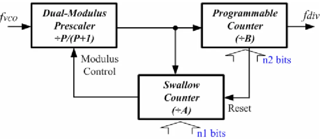
Figure 2.7 shows the generic structure of the full frequency divider (the block “÷N” in Figure 2.6), which consists of a dual-modulus prescaler (DMP), a swallow counter and a programmable counter. The dual-modulus prescaler, which is dedicated to the high-frequency operation, follows VCO so as to relieve the constraint of the operating speed of the counters. The DMP divides by (P+1) until the swallow counter overflows after which the overflow bit (Modulus Control) will set the DMP in divide-by-P mode until the programmable counter overflows. Then, the overflow bit (Reset) will reset both two counters and the division process restarts. Therefore, the overall division ratio becomes (P+1) ·A+P· (B-A) = P·B+A. The detailed discussion of the frequency divider will be presented in section 2.3.
Figure 2.7 A full divider with a dual-modulus prescaler and two counters
2.2.2 Fractional-N
Architecture
As mentioned above, the loop performance of the integer-N architecture is restricted by the given frequency resolution. Compared with the integer-N architecture, however, the fractional-N architecture [11]-[13] shown in Figure 2.8 allows a higher reference frequency for a desired fine frequency resolution. The higher reference frequency implies the wider loop bandwidth, yielding faster settling speed and more suppression of VCO close-in phase noise.
Figure 2.8 A fractional-N frequency synthesizer with an accumulator
A simplified block diagram of a fractional-N frequency synthesizer utilizing an accumulator is shown in Figure 2.9. The accumulator, which consists of an adder and a latch, is clocked by the reference frequency. The output (X+Y) of the adder is latched and then fed to the adder as an input Y. The input X contains the data (K) to be accumulated. When the total (X+Y) exceeds the maximum size (2k) of the adder, an overflow occurs and then the division ratio of the DMP is changed. The DMP divides its input by N when the accumulator is not overflow. When an overflow occurs, the DMP divides its input by (N+1). For every 2k clock cycles, the accumulator overflows K times. Thus, the DMP divides K cycles by (N+1) and 2k-K cycles by N, resulting in an average division ratio: ( 1) (2 ) 2 2 k avg K N k K N K N = ⋅ + + − ⋅ = +N k (2.5)
It can be seen that, therefore, fref can be many times the frequency step resulting in
a higher loop bandwidth without compromising the settling speed and the in-band phase noise. But the periodically alternating process of the DMP causes a sawtooth phase error. This phase error will generate severe spurious tones, which are called “fractional spurs”
at all multiples of the offset frequency (
2k ref K
f
× ) if not filtered. This sawtooth phase
error could be predictable and further eliminated by the classical phase interpolation method [14], as shown in Figure 2.8. This compensation technique requires accurate matching of compensation signals which is sensitive to temperature and process variations. Another solution for large fractional spurs is to randomize the prescaler modulus by using a higher-order Σ-Δ modulator [13]. Its noise-shaping property shapes the noise spectrum of the carrier such that most of the noise energy can appear at large frequency offsets and be pushed outside the loop bandwidth, hence the close-in noise can be suppressed. Arbitrarily fine frequency resolution can be achieved, limited only by the size of the digital adder.
Concerning Σ-Δ Fractional-N PLLs, abundant literatures have been published, and thereby we ends up with the above discussion due to being far away from the focus of this thesis.
2.3 Fundamentals of Phase-Locked Loop (PLL)
When designing a PLL-based frequency synthesizer, it is very important to have the complete knowledge of the behaviors of each functional block as well as the overall closed-loop behavior. As discussed earlier, a charge pump is widely used in PLLs nowadays. Therefore, the following subsections focus on the discussion of integer-N charge pump PLL-based (CPPLL-based) frequency synthesizers.
2.3.1
Phase-frequency Detector (PFD)
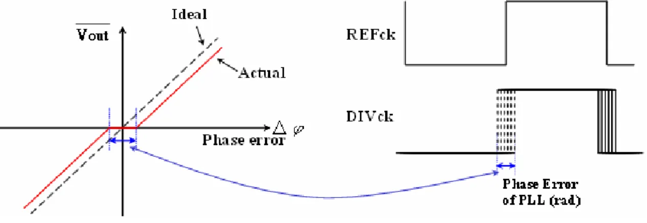
An idea phase detector (PD), as shown in Figure 2.10, produces an output whose average dc value is linearly proportional to the phase difference between its two periodic inputs, namely the reference signal (R)and the divided signal (V).
out PD
v =K ⋅ Δθ (2.6) , where KPD is the gain of the phase detector (specified in V/rad) and Δθ is the input
phase difference.
Figure 2.10 Characteristic of an ideal phase detector
Nowadays, the common phase detectors can be categorized to three types: the analog multiplier-type, the XOR-type, the sequential-type. However, the analog multiplier-type phase detector exhibits the nonlinear dependence of the output voltage on the phase difference and the instability, resulting from the inverted gain polarity beyond the phase difference range, ± π/2. Concerning the XOR-type phase detector, the instability issue still exists except for the nonlinear dependence.
Unlike the multiplier-type and XOR-type, which are only phase-sensitive, the phase-frequency detector (PFD) is a sequential phase detector triggered by else the rise or fall edge of the reference signal (R) and the divided signal (V). As a result, the PFD has the capability of operating as a frequency discriminator for large frequency errors or as a coherent phase detector once inside the pull-in range of the PLL, allowing a fast frequency acquisition and a full linear phase difference range, ± 2π (shown in Figure 2.11).
Figure 2.11 PFD characteristic
As illustrated in Figure 2.12, the operation of a typical PFD is as follows. If initially UP = DN = 0, then a rising transition on R leads to UP = 1, DN remains 0. The circuit remains in this state until V goes high, upon which UP returns to zero simultaneously. The behavior is similar for the V input. Thus, the average dc value of (UP-DN) is an indication of the frequency or phase difference between R and V.
To achieve a PFD with the above behavior, at least, three logical states are required: UP = DN = 0 (state 0); UP = 1, DN = 0 (state I); UP = 0, DN = 1 (state II). Figure 2.13
shows a state diagram summarizing the operations. If the PFD is in the state 0, then a transition on R takes it to state I. During state I, any more rising edge on R won’t changes the state at all. The PFD will remain in this state until a transition occurs on V, upon which the PFD returns to state 0 immediately. The switching sequence between state 0 and state II is similar. Such a PFD is called “tri-state phase-frequency detector”.
Figure 2.13 State diagram of a three-state PFD
2.3.2 Charge
Pump
(CP)
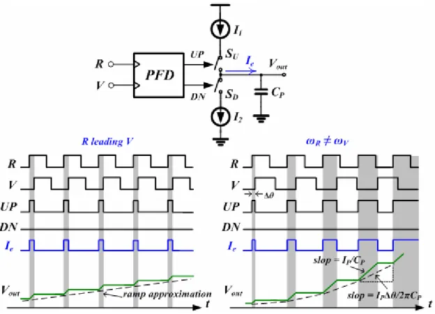
A PFD couldn’t alone provide the exact voltage (or current) signal proportional to the phase difference at its inputs. A charge pump serves to convert the difference of the two output signal UP and DN of the PFD into the corresponding error current either sourced to or sunk from the loop filter, depending on the state of the switches SU and SD
controlled by UP and DN, respectively. No current flows through the loop filter if both switches are off and the output node represents an infinite-impedance towards the loop filter.
A charge pump (CP) with a PFD and a capacity CP as the loop filter is shown in
Figure 2.14, which illustrates the corresponding time-domain response. One should note that the system is nonlinear and discrete time in the strict sense. To overcome this
quandary, it can be approximated by a continuous-time model only when the loop bandwidth is much less than the reference frequency [1]. Therefore, the characteristic of the PFD and charge pump can be together approximated linearly as:
2 e P I I θ π Δ = ⋅ (2.7)
, where Ie is the average error current over a cycle, Δθ represents the phase error between the PFD inputs and IP = I1 =I2 is the current value of the two current sources in
the charge pump.
Figure 2.14 Block diagram of PFD with CP, and the timing diagram
2.3.3
Loop Filter (LF)
The loop filter (LF) determines most of the PLL’s specifications. In CPPLLs, unlike many other feedback systems, the variable of interest changes dimension around the loop: it is converted from phase to current by the PFD/CP, processed by the LF as
such, and then converted back to phase by the VCO. More specifically, the loop filter serves to convert the error current Ie, proportional to detected phase error, into the
corresponding control voltage for VCO. In general, the loop filter can be realized in either active or passive forms, and its design has a great impact on the overall system performance of CPPLLs, such as the loop stability and noise rejection. The stability issue of great concern tends to apply for low order filters, which conflicts with the noise-rejection requirement. Figure 2.15 shows three features of the passive filter commonly adopted in most CPPPLs, namely first-order, second-order, and third- order filters, respectively.
Figure 2.15 Different features of the passive filter
2.3.4 Voltage-Controlled
Oscillator
(VCO)
Figure 2.16 VCO characteristic
An ideal voltage-controlled oscillator, as shown in Figure 2.16, is a circuit that generates a periodic output whose frequency is a linear function of a control voltage
(Vctrl):
2
out free KVCO Vctrl
ω =ω + π ⋅ (2.8) Here, ωout represents the free-running frequency, and KVCO denotes the “gain” of the
VCO or “sensitivity” of the circuit (specified as Hz/V). Since the phase is the integral of frequency with respect to time, the output signal of a sinusoidal VCO can be expressed as
( ) cos free 2 VCO t ctrl( )
y t A ω t πK V t dt
−∞
⎡ ⎤
= ⋅ ⎢ + ⎥
⎣
∫
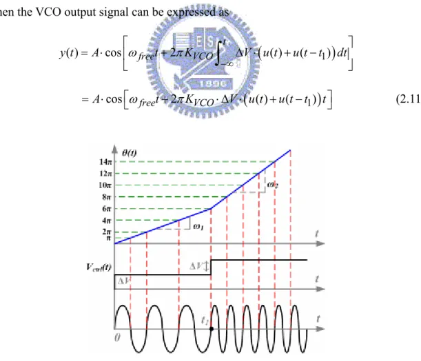
⎦ (2.9)As depicted in Figure 2.17, for example, if applying a step voltage as follows:
(
1)
1( ) ( ) ( ) , 0
ctrl
V t = Δ ⋅V u t +u t t− t > (2.10) , then the VCO output signal can be expressed as
(
1)
( ) cos free 2 VCO t ( ) ( )
y t A ω t πK V u t u t t dt
−∞
⎡ ⎤
= ⋅ ⎢ + Δ ⋅ + − ⎥
⎣
∫
⎦= ⋅A cos⎣⎡ωfreet+2πKVCO⋅ Δ ⋅V u t
(
( )+u t t( − 1))
t⎤⎦ (2.11)Thus, as expected, when t = 0, Vctrl experiences a voltage step ΔV and then the
VCO frequency is simply shifted up by 2πKVCOΔV. When time goes to t1, the frequency
is shifted up by 2πKVCOΔV again. The illustration reveals that, the higher the VCO
frequency, the faster the VCO phase accumulates. However, in the analysis of PLLs, the VCO is viewed as a linear time-invariant system whose input and output are the control voltage (Vctrl) and the output excess phase ( ), respectively. Thus,
the input-output transfer function is
2πKVCO t Vctrl t −∞
∫
( )dt 2 ( ) out VCO ctrl K s V s θ = π (2.12)2.3.5 Frequency
Divider
As discussed earlier, the output frequency of a PLL-based frequency synthesizer is fout=N· fref. Thus, with a fixed reference frequency, the controllability of the output
frequency or channel selection depends on the controllability of the division ratio N. In order to achieve such a channel selection function, a frequency divider with full programmability of N in an arbitrary range serves to change the output frequency of the VCO according to the digital channel-selection control input.
Such a programmable frequency divider can be easily implemented with standard CMOS logic, for example, a digital programmable counter. However, with the growth of wireless communication systems, the wireless frequency band goes higher, i.e. over GHz. Thus, it is not an easy task to realize such a divider completely in standard CMOS logic, especially for a high-moduli divider. Even if the process technology evolves so that such a digital counter could operate at GHz range, the considerable power consumption prevents one from using it in most PLL designs. Usually, a simple prescaler is hence used in the front to lower the operating frequency of the actual programmable divider. Depending on the system constraints, two different types of prescalers are used: fixed modulus and dual modulus.
(a) (b)
Figure 2.18 Different types of prescaler: (a) fixed modulus, and (b) dual modulus
The simplest implementation of the prescaler is the first-type fixed modulus high-speed prescaler, as shown in Figure 2.18 (a). The purpose of such a high-speed architecture is to lower the frequency to some extent before the actual programmable divider. However, dividing the output frequency by a fixed factor V means N can only be chosen in steps of V. This could, of course, be compensated by decreasing the reference frequency by the same factor, resulting in a narrow loop bandwidth. This would yield slower settling of PLL’s transients and less suppression of the VCO close-in phase noise. Also, a lower reference frequency implies a higher division ratio. The noise of the reference oscillator, PFD, CP, and LF is seen in the output of PLLs multiplies by N. Thus, increasing N would tighten the requirements for the rest of the PLL building blocks. So, such a fixed prescaler can only operates in systems which allow long switching times between frequency changes.
Due to the drawbacks of the fixed modulus prescalers, instead, dual-modulus prescalers (DMPs) are almost always preferred. Having two possible moduli instead of one increases the circuit complexity only slightly, and none of the problems of increasing N and decreasing the reference frequency occur in this case. In general, two types of DMPs are developed: conventional dual-modulus architecture and phase switching architecture. Nevertheless, only the dual-modulus architecture is the focus of our concern in this work. Accordingly, our work will concentrate on the popular
pulse-swallow frequency divider, which consists of a DMP, a swallow counter and a programmable counter, as shown in Figure 2.18 (b). The two counters used here are n1-bit and n2-bit counter, respectively.
Figure 2.19 illustrates the timing diagram of the whole frequency divider. If Mode = 1, the input frequency from VCO, fVCO, is divided by (P+1) by the DMP. In this
instant, both the counters begin to counter. After the n1-bit swallow counter counts “A”
clocks, it will overflow and output a control pulse to set Mode from 1 to 0. Once Mode is set to 0, the DMP alters to divide by P and the swallow counter is disabled. Then, only the n2-bit programmable counter keeps on count in this mode. After the
programmable counter counts the residual “B-A” pulses, it will overflow and reset both two counters. Besides, the DMP will be set back in divide-by-(P+1) mode and then a new division cycle begins. During a period of the divided output signal, there are (P+1) ·A+P· (B-A) = P·B+A input clocks enter the DMP. In other words, fVCO =
(P·B+A) ·fdiv.
2.4 Modeling and Analysis of Frequency Synthesizer
A PLL is a negative feedback system that operates on the excess phase of nominally periodic signals. Duet to the sampling and switching nature of the PFD/CP, the transient response of PLL is generally a nonlinear phenomenon. Although the PLL is a highly nonlinear system, it has been found that when the loop is in lock and its state changes by only a very small amount on each cycle of the input, it can be reasonably well approximated as a linear system [1]. With this linear approximation, a several Laplace transfer functions will be derived to gain insight into trade-offs in PLL design and the performance of PLLs, such as loop stability, static phase error, and transient response in this section.
2.4.1 Loop
Stability
Analysis
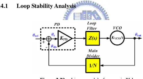
Figure 2.20 Linear model of a generic PLL
Figure 2.20 illustrates a linear model of a generic PLL. Note that the input and output variables of the PLL are phases. The phase detector compares the phase of the input reference signal θref and the phase of the divided signal θdiv. It produces a phase
error θe, and then converts this phase error with a gain KPD (i.e. IP/2π for CPPLLs) into a
corresponding error signal Ve(s) or Ie(s). That is,
( ) [ ( ) ] ( )
e PD ref div PD e
Then, the loop filter Z(s) filters the error signal Ve(s) and produces the VCO control
voltage Vctrl(s), equal to:
( )Vctrl s =Z s V s( )⋅ e( ) (2.14) Recall from (2.12) that the VCO is modeled as a phase integrator. This results in an output excess phase θout as follows:
2
( ) ( ) VCO
out s Vctrl s πKs
θ = ⋅ (2.15)
In turns, this output phase θout(s) is fed back and passes through the frequency divider.
Because frequency and phase are related by a linear operator, division of frequency by a factor of N is identical to division of phase by the same factor. Thus, the feedback phase θdiv is
( ) ( ) out
div s θ N s
θ = (2.16)
The open-loop transfer function can be expressed as follows:
2 1 ( )open ( ) ( ) PD ( ) KVCO H s A s s K Z s s N π β = = ⋅ ⋅ ⋅ (2.17)
As with other feedback systems, A(s) is the forward-loop gain and β(s) is the reverse-loop gain. This open-loop transfer function determines the performance of the PLL, such as the loop stability.
Shown in Figure 2.21 (a) is the linear model of a CPPLL. Firstly, if only a single capacity is employed as the loop filter, Equation 2.17 becomes
1 ( )open P VCO p K I H s N sC s ⎛ ⎞ = ⎜⎜ ⎟⎟ ⎝ ⎠ (2.18) Since the loop gain has two poles at the origin, this topology is called a “type-II second-order PLL”. As shown in Figure 2.21 (b), due to two poles at the origin, (i.e. two ideal integrators), each integrator contributes a constant phase shift of 90° and hence the phase margin is zero at the gain crossover frequency, yielding instability.
(a) (b)
Figure 2.21 (a) Linear model of a 2nd order CPPLL and (b) its open-loop Bode plot.
In order to stabilize the system, a zero must be introduced in the loop gain such that the phase shift is less than 180° at the gain crossover frequency (Figure 2.22 (b)). As shown in Figure 2.22 (a), this can be accomplished by adding a resistor RP in series
with the capacity CP. Thus the open-loop transfer function can be rewritten as
2
1
( )open P P VCO P VCO P z
P K I K R I s H s R N C s s N s ω ⎛ ⎞ ⎛ + ⎞ = ⎜ + ⎟ = ⎜ ⎝ ⎠ ⎝ ⎠ ⎟ (2.19) , where a zero at z 1 P P R C ω = − .
The loop bandwidth K, defined as the unity gain frequency of the open-loop transfer function, can be found out assume that K is much greater than ωz:
2
1
( )open I KP VCO PR s z I KP VCO PR 1
H s N s N ω ⎛ + ⎞ ⎛ ⎞ = ⎜ ⎟≈ ⎜ ⎟ ⎝ ⎠ ⎝ ⎠ s = P VCO P I K R K N ⇒ = (2.20)
As the Bode plot indicates, if IPKVCO increases, the gain crossover frequency
(namely, the loop bandwidth K) moves away from the origin, enhancing the phase margin. But since the PFD/CP works in discrete time domain, the loop bandwidth should be considerably lower than the reference frequency according to Gardner’s stability limit [1]. In other words, the loop gain should be limited to avoid instability.
(a) (b)
Figure 2.22 (a) Linear model of a compensated 2nd order CPPLL and (b) its open-
loop Bode plot.
Besides, this compensated type-II second-order PLL suffers from a critical drawback. Since the charge pump drives the series combination of RP and CP, each time
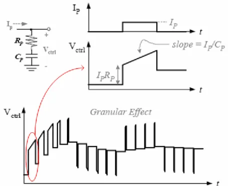
a current is injected into the loop filter, the control voltage experiences a large jump of IPRP, as shown in Figure 2.23. So, the PLL suffers from serious “granularity effect”,
which can be seen easily in transient response (Figure 2.23). A possibly more serious problem introduced by the jumps is the potential for overload of the VCO. More specifically, any real VCO has only a finite frequency range over which it can be tuned. If this voltage jump exceeds the valid input control range of VCO, it leads to the failure of the operation of the overall charge pump PLL.
Additionally, any possibly mismatches in the CP introduce voltage jumps in Vctrl
even in the locked status. The resulting ripple severely disturbs the VCO, which causes large spurs. To alleviate these issues, a second capacity is added in shunt with the first-order filter. Now, the loop filter is of second-order, yielding a third-order PLL, which is adopted in our work.
Shown in Figure 2.24 is the type-II third-order PLL that alleviate the voltage- jump-induced problems stated above. The transfer function of the loop filter now becomes
Figure 2.23 Granular transient response of a PLL with first-order loop filter
(
)
2 2 1 ( ) / 1 1 / 1 P P P f P P p P P C sR C s Z s K C C sC sRC s s C C z ω ω + + = ⋅ = ⋅ + ⎛ ⎞ + + ⎜ + ⎟ ⎝ ⎠ (2.21) , where z 1 P P R C ω = , 2 2 P p P P C C C C R ω = + , 2 P P f P C R K C C = +Note that a new pole ωp is introduced with its frequency higher than the zero ωz
according to the following formula:
2 1 P p z CC ω =ω ⎛⎜ + ⎞ ⎝ ⎠⎟ (2.22)
Substitute Equation 2.20 into Equation 2.17 and then the open-loop transfer function can be written as
(
)
2 ( ) ( ) / 1 P VCO f VCO P z open p I K K K I s H s Z s N s N s s ω ω + = = ⋅ + (2.23)The phase margin is then given by
1 1
tan ( / z) tan ( / )
Figure 2.24 Linear model of a type-II 3rd order CPPLL
Figure 2.25 Open-loop Bode plot of type-II 3rd order CPPLL
The open-loop Bode plot is shown in Figure 2. 25. The phase of H(s)|open is -180° at dc.
The zero ωz and the pole ωp introduce phase shifts of +90 ° and -90°, respectively. Thus,
it is essential to place the gain crossover frequency K between ωz and ωp for enough
phase margin in consideration of stability. To find out the value of K that satisfies the optimal phase margin, equaling the derivative of the phase margin to zero gives
(
1 1)
2 2 2 2 tan ( / z) tan ( / p) z p 0 z p d d ω ω ω ω ω ω ω − − − =ω +ω −ω +ω = opt z p Kopt ω ω ω ⇒ = = (2.25) That is, if the loop bandwidth is set to the geometric average of ωz and ωp, the phaseFurthermore, we defines a new parameter γ as p z K K ω γ ω = = (2.26)
Table 2.1shows a useful reference table of the relationship between γ and PM. From Equation 2.21, the capacitance ratio of CP and C2 can be represented by
2 2 1 P C C =γ − (2.27) Assume the loop bandwidth K is much greater than ωz but much smaller than ωp. K can
be found out:
(
)
2 2 ( ) 1 / 1 P VCO f z P VCO f open p I K K s I K K s H s N s s N s ω ω + ⎛ ⎞ = ≈ ⎜ ⎟ + ⎝ ⎠= 2 P VCO f P VCO P P P I K K I K R C K N N C ⇒ = = + C (2.28) Table 2.1Relationship between γ and PM
γ PM 1 0º 2 36.9º 3 53.1º 4 61.9º 5 67.4º

![Figure 1.7 (a) The proposed PFD architecture [8]; (b) Its phase-detection characteristic](https://thumb-ap.123doks.com/thumbv2/9libinfo/8226189.170749/22.892.129.763.453.774/figure-proposed-pfd-architecture-b-phase-detection-characteristic.webp)