國
立
交
通
大
學
電信工程學系
碩
士
論
文
尾電流塑形低相位雜訊暨
電流共用低功率四相位輸出壓控振盪器設計與研究
Design of Tail Current-Shaping Low Phase Noise QVCO and
Current-reused Low Power QVCO
研究生:黃子哲
指導教授:周復芳 博士
尾電流塑形低相位雜訊暨
電流共用低功率四相位輸出壓控振盪器設計與研究
Design of Tail Current-Shaping Low Phase Noise QVCO and
Current-reused Low Power QVCO
研 究 生:黃子哲 Student:Tze-Che Huang
指導教授:周復芳 博士 Advisor:Dr. Christina F. Jou
國 立 交 通 大 學
電 信 工 程 學 系 碩 士 班
碩 士 論 文
A Thesis
Submitted to Department of Communication Engineering College of Electrical Engineering and Computer Science
National Chiao Tung University In Partial Fulfillment of the Requirements
for the Degree of Master of Science in Communication Engineering
June 2009
Hsinchu, Taiwan, Republic of China
I
尾電流塑形(Tail Current-Shaping)低相位雜訊暨
電流共用低功率四相位輸出壓控振盪器設計與研究
研究生:黃子哲 指導教授:周復芳 博士國立交通大學電信工程學系碩士班
摘 要
本論文討論分為兩部份,第一部份為利用尾電流塑型技巧達成低相位雜訊目地之四 相位輸出壓控振盪器,第二部份為利用電流共用架構達成低功率消耗之四相位輸出壓控 振盪器。在第一部份,我們利用了兩個差動輸出一階諧波鎖相振盪器建構出一尾電流塑 形四相位輸出壓控振盪器。利用此振盪器之輸出訊號作為尾端電流源之電晶體閘極端的 交流輸入訊號我們可以達成降低相位雜訊之目地。本四相位壓控振盪器由 TSMC 0.18μm mixed-signal/RF CMOS 1P6M 製程實現,晶片面積為 0.7x1.1 mm 。量測結果顯示出: 本壓控振盪器之振盪頻率為 5.28GHz,在供應電壓為 1.4V 之條件下損耗功率為 11.2mW, 相位雜訊為-119.3dBc/Hz@1MHz。 第二部份本論文提出一電流共用架構來降低壓控振盪器之功率消耗。藉由此共用電 流之方法,我們可將振盪器之功率消耗降至為原先的二分之一。我們將兩差動輸出電流 共用振盪器利用背閘極耦合(Back-Gate Coupling)方式建構出一四相位輸出振盪器來達 成低功率損耗之目地。模擬結果顯示:本壓控振盪器之振盪頻率為 10GHz,在供應電壓 為 1.2V 之條件下損耗功率僅為 1.64mW,相位雜訊為-111.7dBc/Hz@1MHz。II
Design of Tail Current-Shaping Low Phase Noise QVCO and
Current-reused Low Power QVCO
Student: Tze-Che Huang Advisor: Dr. Christina F. Jou
Department of Communication Engineering
National Chiao Tung University
ABSTRACT
This thesis discusses about designs of tail current-shaping low-phase noise QVCO and current-reused low power QVCO. In the first part, we present a new tail current-shaping quadrature voltage-controlled oscillator (QVCO) which consists of two first-harmonic injection-locked oscillators (ILOs). The outputs of the proposed QVCO are injected back to the gates of the QVCO’s tail transistors in order to shape the tail current. With the implementation of tail current-shaping, the RMS value of the effective impulse sensitivity function (ISF) of the proposed QVCO is 40% smaller than the conventional QVCO topology. The proposed CMOS LC-tank QVCO has been implemented with the TSMC 0.18μm mixed-signal/RF CMOS 1P6M technology and the die area is 0.7x1.1 mm . The total power consumption is 11.2 mW at the supply voltage of 1.4 V. The measured phase noise at 1MHz offset is -119.3dBc/Hz at the oscillation frequency of 5.28 GHz and the figure of merit (FOM) of the proposed QVCO is about -183dBc/Hz.
In the second part, we propose a current-reused QVCO topology to reduce the power consumption. In our design, the proposed QVCO consists of two NMOS current-reused differential VCO. The qudra-phase signals are coupled by back-gate coupling technique. Therefore, the power consumption of the proposed QVCO can be cut in half by reusing the dc
III
currents compared to the conventional QVCO topologies. The simulated results show that the total power consumption is about 1.64 mW since the QVCO core circuit draws 1.37 mA from a 1.2 V V supply. The simulated phase noise at 1 MHz offset is-111.7dBc/Hz at the oscillation frequency of 10 GHz and the FOM is about -189.6dBc/Hz.
IV
誌 謝
時光飛逝,兩年碩士班生涯匆匆的就過去了,回首過程的點滴,才發現許多回憶和 經歷都是值得回味的。從高中畢業決定專業志向至今一路走來,首要感謝的是我的父母 對我全心的信任以及全方位的支持,感謝你們陪我走過求學歷程中的許多起伏,在我小 有成就時給予我極大的鼓勵,在我面對挫折時對我不求回報的包容,對於這份親情的付 出我此生都無以回報,只能在此表達我對你們由衷的感謝。此外要感謝的還有關心我的 親人們,感謝我的弟弟子晏,即便遠在太平洋的另一端仍不時的給我關心支持,感謝我 的奶奶及其它親人們,你們對我的期許是我前進的動力,感謝我的女友顗如,在我最需 要妳的時候與我相逢,改變了我的態度及生活,因為擁有妳的笑容,才讓我有力量面對 生活的一切。 此外在成長的歲月裡,特別要感謝我的好朋友們。最要感謝的是我的學長種馬,從 大學時代就不斷的鼓勵我,我們擁有相同的想法及抱負,一起成長一起前進,倘若沒有 遇見你,必定不會有今日的我。另外感謝小白、佳蓉、彥期以及我其它的好朋友們,感 謝你們在我低潮時對我的包容及鼓勵,許多次與你們長談,都深遠的影響了我,你們是 我最大的無形財富。 最後要感謝的是在碩士班的日子裡,我的指導教授周復芳博士在專業上給予我的指 導,感謝周復芳老師在研究領域裡給我很大的自由發展空間,並且適時的給予我建議及 鼓勵。另外感謝昱舜、宜星、沛遠、志豪及其它學長們在研究上給予我許多的指導和經 驗的分享,無不帶給我莫大的幫助。感謝碩二的夥伴們昭維、奕霖、玠瑝、宗廷在這兩 年中與我一起學習成長,以及 919 實驗室的學長學弟們陪伴我渡過這兩年美好的時光。 黃子哲 於 風城 2009,JulyV
CONTENTS
C hi ne s e Abs tr ac t I
E ng l i s h A b s t r a c t I I
Ac kn owl e d ge me nt I V
C o n t e n t s V
List of Table VII
List of Figure VIII
Chapter 1 Introduction…..………1
1.1 Background and Motivation………..………1
1.2 Thesis Organization……..…...………..…….……..3
Chapter 2 Tail Current-Shaping Low-Phase Noise QVCO………..………...…..…4
2.1 Introduction………..……….4
2.2 Circuit Design Consideration………..………...………...6
2.2.1 Tail Current-Shaping Technique……….6
2.2.2 The LC Tank Design………....………13
2.2.3 Forward Body Bias………...………15
2.3 Chip Layout and Simulation Results……….……….…….17
2.4 Measurement Results and Discussion…………..………...20
2.4.1 Measurement Consideration………...…...……...20
2.4.2 Measurement Result………...………..………21
Chapter 3 Current-Reused QVCO………...………...……….25
3.1 Introduction……….………25
3.2 Circuit Design Consideration…………..……….………...27
VI
Chapter 4 Conclusion and Future Work………..………35 4.1 Conclusion……….………..35 Reference………...………...36
VII
LIST OF TABLE
Table 1-1 Wireless communication system characteristic………...2 Table 2-1 Comparison of additional capacitance………...14 Table 2-2 QVCO simulated performance in different corner condition………...……19 Table 2-3 comparison between simulation and measurement………..24 Table 2-4 comparison between this work and references……….24 Table 3-1 the comparison between the proposed QVCO and references…..………...34
VIII
LIST OF FIGURE
Figure 1-1 DS-UWB spectrum allocation………..2
Figure 1-2 Multi-band spectrum allocation………3
Figure 2-1 Circuit schematic of a differential VCO………...….4
Figure 2-2 Conventional cross-coupled VCO………...…….6
Figure 2-3 Conventional cross-coupled VCO with a capacitance which paralleled to the tail transistor M ………...7
Figure 2-4(a) First-harmonic injection-locked oscillator………...…9
Figure 2-4(b) the waveforms of VCO’s outputs and tail current………...9
Figure 2-5(a) the proposed QVCO with tail current-shaping………...10
Figure 2-5(b) the waveform of the tail currents………...10
Figure 2-6(a) the outputs voltage waveform without C1~C4………....13
Figure 2-6(b) the outputs voltage waveform with C1~C4………...13
Figure 2-7 the waveform of tail currents………...14
Figure 2-8 IV curve of the MOSFET with and without FBB………...15
Figure 2-9 Drain current of the MOSFET with FBB………...16
Figure 2-10 Chip layout of the proposed QVCO………...17
Figure 2-11 the phase noise of the proposed QVCO………..…..17
Figure 2-12 Tuning range of the proposed QVCO………...18
Figure 2-13 the outputs waveform of the proposed QVCO………...19
Figure 2-14 Bias-Tee model………...20
Figure 2-15(a) SSA(Agilent E5052A)………..…...…20
Figure 2-15(b) down-converter(Agilent E5053A)………...………20
IX
Figure 2-17 the measured phase noise of the proposed QVCO………...22
Figure 2-18 the outputs spectrum of the proposed QVCO………...22
Figure 2-19 the tuning range of the proposed QVCO………...23
Figure 2-20 the outputs voltage waveform of the proposed QVCO………23
Figure 3-1(a) the conventional VCO………...….25
Figure 3-1(b) the current-reused VCO………..…...25
Figure 3-2 the current reused differential VCO………….………..…27
Figure 3-3(a) the proposed current reused QVCO………...28
Figure 3-3(b) the small signal equivalent circuit of switching transistor M …….….28
Figure 3-4(a) a conventional parallel-coupled QVCO………...…..30
Figure 3-4(b) the small signal equivalent circuit of M and M ……….…………30
Figure 3-5 the simulated phase noise of the proposed QVCO……….32
Figure 3-6 the simulated tuning range of the proposed QVCO………...33
Figure 3-7 the outputs voltage waveform………...33
1
Chapter 1 Introduction
1.1 Background and Motivation
In the last years, the requirements of low-cost and low-power for wireless system have dramatically increased due to the continuous growth of personal wireless communications. Wireless transceivers for many standards, including GSM, Bluetooth, WLAN require low-power design techniques to enhance their battery lifetime and to improve their portability. For radio frequency integrated circuit (RFIC) designers, a low-power and high-integration design is a great concern.
In the wireless transceiver blocks, phase-locked loops (PLL) are widely utilized such as frequency synthesizers and clock sources. Since the voltage-controlled oscillators (VCO) play a key role in the PLL circuits and the phase noise of the VCO directly affect the performance of the PLL circuits, the low-power and low-phase noise of VCOs are required. Due to the requirements of quadrature local oscillator (LO) generation for up- and down-conversions with image-reject mixing in the wireless transceiver blocks, a quadrature VCO (QVCO) with accurate quadra-phase outputs is a general design.
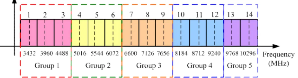
In 2002, the Federal Communications Commission (FCC) has allocated 7500-MHz of spectrum for ultra wideband (UWB) system in 3.1~10.6 GHz [1]. According to FCC’s definition, UWB system occupied a bandwidth is equal to or greater than 500MHz when the center frequency is over than 2.5GHz, or has a fractional bandwidth is equal to or greater than 20 % of the center frequency when the center frequency is less than 2.5GHz. There are two proposals for UWB system: DS-CDMA (Direct-Sequence Code Division Multiplexing Access) and MB-OFDM (Multi-Band Orthogonal Frequency Division Multiplexing).
2
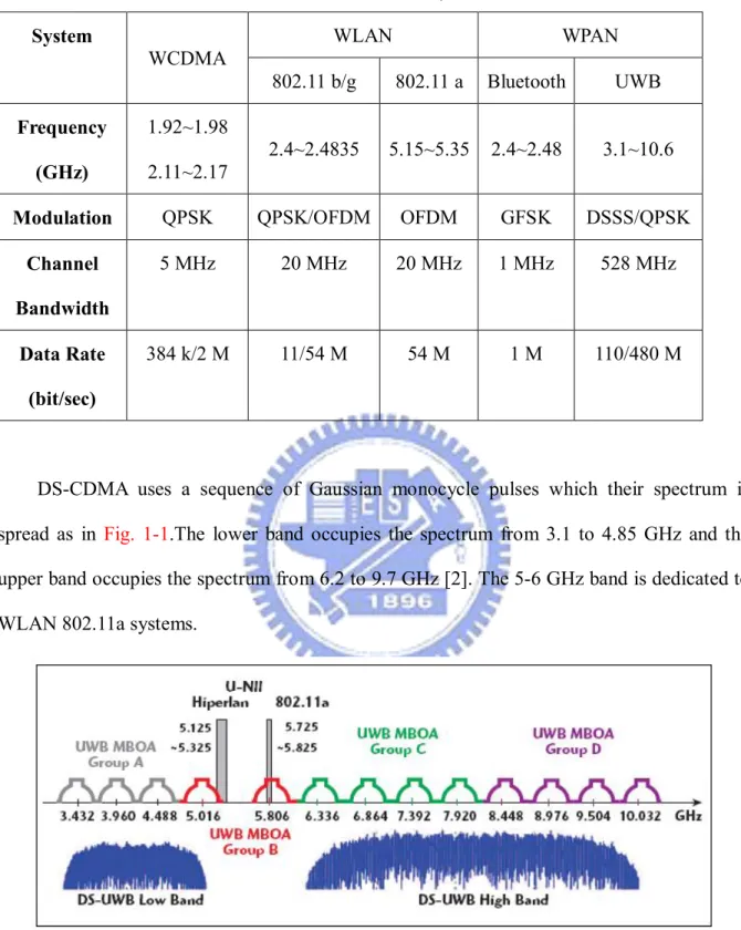
Table 1-1 Wireless communication system characteristic
System WCDMA WLAN WPAN 802.11 b/g 802.11 a Bluetooth UWB Frequency (GHz) 1.92~1.98 2.11~2.17 2.4~2.4835 5.15~5.35 2.4~2.48 3.1~10.6
Modulation QPSK QPSK/OFDM OFDM GFSK DSSS/QPSK
Channel Bandwidth 5 MHz 20 MHz 20 MHz 1 MHz 528 MHz Data Rate (bit/sec) 384 k/2 M 11/54 M 54 M 1 M 110/480 M
DS-CDMA uses a sequence of Gaussian monocycle pulses which their spectrum is spread as in Fig. 1-1.The lower band occupies the spectrum from 3.1 to 4.85 GHz and the upper band occupies the spectrum from 6.2 to 9.7 GHz [2]. The 5-6 GHz band is dedicated to WLAN 802.11a systems.
Fig. 1-1 DS-UWB spectrum allocation
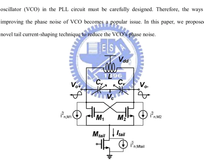
See Fig. 1-2. In M-B-OFDM UWB, frequency span is grouped into five major band groups which are in turn sub-divided into 14 bands in total, each band is 528 MHz bandwidth [3].
3
Fig. 1-2 Multi-band spectrum allocation
1.2 Thesis Organization
In this thesis, a quadrature voltage-controlled oscillator for WLAN 802.11a is implemented by using TSMC RF 1P6M 0.18 μm CMOS technology, and a very low-power QVCO operating at 10 GHz oscillation frequency has been proposed.
Chapter 2 will introduce a low-phase noise QVCO. In order to improve phase noise, we utilizing tail current-shaping technique and forward-body bias technique to decrease the phase noise.
Chapter 3 will propose a very low-power QVCO, which is a novel current-reused topology. We also utilized back-gate coupling technique not only to reduce the power dissipation but also to improve the phase noise.
Chapter 4 will give some discussions of these proposed QVCOs to compare the measured results with the simulation results and the references. A conclusion about this thesis is proposed in the end.
4
Chapter 2 Tail Current-Shaping
Low-Phase Noise QVCO
2.1 Introduction
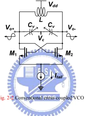
Phase-locked loop (PLL) circuits play a very important role in radio-frequency (RF) transceiver system. In order to generate a low phase noise local clock, the voltage-controlled oscillator (VCO) in the PLL circuit must be carefully designed. Therefore, the ways of improving the phase noise of VCO becomes a popular issue. In this paper, we proposed a novel tail current-shaping technique to reduce the VCO’s phase noise.
Fig. 2-1 Circuit schematic of a differential VCO
The main contributors to the phase noise of a conventional differential VCO, as shown in
Fig. 2-1, are the cross-coupled devices(M and M ) and tail transistor(M ). , and
5
of the tail transistor. The low-frequency device noise can be up-converted to the high-frequency phase noise of the oscillator. Depending on the state of the oscillator, current noise present in these components is converted more efficiently into phase noise. Refer to the impulse sensitivity function (ISF) [4], the impact of any noise source on the oscillator phase noise varies across oscillation period. By shaping the tail current I , we can decrease the active time of the noise source to reduce the oscillator phase noise. There are many tail current-shaping skills were proposed to reduce the device noise up-converting to VCO’s phase noise, one method was brought up that is to couple the oscillating signal to the tail current source of VCO as an inductor, which will spend large chip area [5]. Another way of current-shaping is to input an additional pulse into the gate of tail transistor. However, it’s not a convenient way to inject an additional pulse signal into our circuit, although the phase noise reduction of this manner had been mathematically proved [6].
Instead of generating an additional pulse as the injection signal or spending extra chip area, we build a quadrature VCO (QVCO) with two first-harmonic injection locked structure [7] and use the QVCO’s own outputs signals as a self-injection signal to shape the tail current I . This paper proposed a novel QVCO circuit implemented in the TSMC 0.18 μm CMOS 1P6M technology and operating at 5.3 GHz oscillation frequency. The quadra-phase outputs of the oscillator are coupled by 4 PMOS in series, and the tail current source injection signals come from the QVCO’s outputs signals. We also use forward body bias (FBB) technique to reduce the supply voltage. Therefore, a tail current-shaping QVCO, which reaches low phase noise, can be obtained.
6
2.2 Circuit Design Consideration
2.2.1 Tail Current-Shaping Technique
A. the phase noise analysis of a conventional VCO
Fig. 2-2 Conventional cross-coupled VCO
Fig. 2-2 shows a conventional differential VCO. As mention in introduction before, the main contributors to the phase noise of this VCO are the cross-coupled devices ( M and M ) and the tail current source ( I ). It is because that the low-frequency device noise can be up-converted to the high-frequency phase noise of the oscillator. Because of the phase noise in the single-ended and the differential signals are identical, we therefore use a single-ended phase noise analysis to keep the equations simple. The thermal current noise
power spectral density of transistor M can be expressed as , ∆ = 4 , when
M is conducting current, and it is close to zero when the transistor is OFF and highly resistive; , is the transconductance of M , and is a coefficient related to device size.
7
The effective ISF of M can be expressed as Γ , ( ) = Γ ( ) ( ), where ( ) is the noise modulation waveform [4]. When Γ = sin(φ) [8], the RMS value of the effective ISF becomes Γ , , = 1 2π Γ (φ)α (φ) φ = 1 2π sin φ φ = 1 4 (1)
B. the phase noise analysis of a VCO with parallel capacitance to the tail
transistor for current-shaping
Fig. 2-3 Conventional cross-coupled VCO with a capacitance which paralleled to the tail transistor
Fig. 2-3 shows a conventional differential VCO with a NMOS tail current transistorM . To improve the oscillator’s phase noise, a capacitance C is connected with the tail transistor in parallel for the tail current-shaping. The voltage at the tail node will be a sinusoid of frequency2ω , where ω is the oscillating frequency. Therefore, the tail current can be expressed as
8
I = I − 2ω sin(2 − ) (2)
I is the DC value of the tail current, is its amplitude, and is its phase delay compared to the output voltage V and V . By designing the size of the devices, we can let θ = π 2⁄ and 2ω = and the tail current will become
I = I (1 + cos(2ω t)) (3)
With this sinusoidal signal, the power spectral density of the thermal current noise becomes ∆ = ∆ 2(1 + cos(2φ)) = ∆ α (φ), and the noise modulation function α (φ) = 2(1 + cos(2φ)). Therefore, the RMS value of ISF of M can be showed as
Γ , , = 1 2π Γ (φ)α (φ) φ = 1 2π sin (φ) 2(1 + cos(2φ)) φ = 2 3π (4)
, which is about 15% smaller than (1). Therefore, up-conversion noise from cross-coupled device and tail current can be further reduced with the tail current shaping technique [6, 9].
9
C. the proposed QVCO design
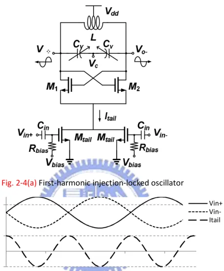
Fig. 2-4(a) First-harmonic injection-locked oscillator
Fig. 2-4(b) the waveforms of VCO’s outputs and tail current
Fig. 2-4
In this design, we propose a QVCO with a new tail current-shaping technique so as to improve the phase noise. The proposed QVCO is based on two first-harmonic injection-locked oscillators (ILOs) and utilize the QVCO’s own output signals as a self-injection signal to shape the tail current.
Fig. 2-4(a) shows the ILO structure, the external injection signals V and V are injected into the gates of the tail current transistor pair M . The ILO structure can be considered as a simple doubler, therefore, the tail current signal with frequency 2ω
Vin+ Vin-Itail
10
can be obtained (ω is the oscillating frequency of the VCO). See Fig. 2-4(b), the sinusoidal tail current of 2ω frequency is aligned with the zero-crossing point of the out-of-phase signals V and V .
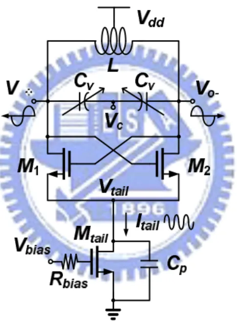
Fig. 2-5(a) the proposed QVCO with tail current-shaping
Fig. 2-5(b) the waveform of the tail currents
11
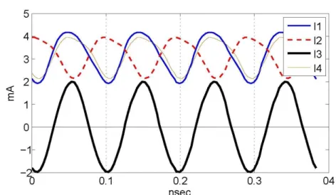
Fig. 2-5(a) shows the proposed QVCO, the PMOS pairs (M and M , M and M ) at the top of the circuit were used to couple the two ILOs in quadrature phase [10]. By injecting the quadra-phase outputs signals (I and I , Q and Q ) back to the gates of the tail transistors M as shown in Fig. 2-5(a), the tail currents of ILOs can be shaped at frequency 2ω without external signals. However, the currents of tail transistor pairs I and I would have asymmetric waveforms, it is because of the parasitic capacitance at the drain of tail transistors. To eliminate the asymmetric phenomenon, the connection between two tail transistor pairs offers a path I for tail currents switching. Fig. 2-5(b) shows the simulation result of the relationship between the tail currents I , I , I , and I . The waveforms of the currents I and I , which pass through the tail transistor pairs, have out-of-phase relationship because of the quadrature phase injection signals I and Q. By the switching current I between I and I , the asymmetric phenomenon of I and I can be canceled by each other, therefore, a symmetric waveform can be obtained at the tail current I . The sinusoidal tail current I of the ILO which is aligned with the zero-crossing point of I and I can be expressed as
I = I (1 + sin(2ω t)) (5)
In this proposed QVCO, the thermal current noise power spectral density of M can be expressed as
∆ = ∆ 2(1 + sin(2φ)) = ∆ α (φ) (6)
And the RMS value of effective ISF can be obtained as
Γ , , = 1 2π Γ (φ)α (φ) φ = 1 2π sin (φ) 2(1 + sin(2φ)) φ = √2 3π (7)
, which is about 40% smaller than (1). By shaping the tail currents of ILOs, the phase noise contribution from the cross-coupled devices and tail transistors can be minimized. The ADS
12
simulation results showed that the proposed QVCO’s phase noise is -120 dBc/Hz @ 1 MHz offset frequency.
13
2.2.2 The LC Tank Design
In the design of the proposed QVCO’s LC tank, we add 4 capacitances ~ as shown in Fig. 2-5(a) to increase the amplitude of the outputs waveform. The equivalent capacitance of the LC tank = + , and the oscillating frequency ω becomes
.
(a) The outputs voltage waveform without ~
(b) The outputs voltage waveform with ~ Fig. 2-6
14
Fig. 2-6 shows the comparison of the outputs voltage waveform between the condition within and without the additional capacitances ~ . The amplitude of the outputs waveform within ~ is 26% larger than the one without the additional capacitances.
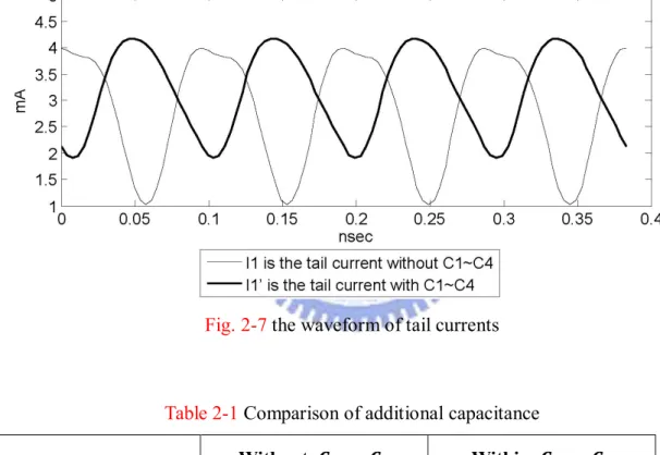
Fig. 2-7 shows the waveforms of the tail current in Fig. 2-5(a), and the amplitude of is a equation about ~ [11]. By adjusting the value of the additional capacitances ~ , we made match to equation (5) to obtain better current-shaping effect, and the phase noise can also be improved as shown in Table 2-1.
Fig. 2-7 the waveform of tail currents
Table 2-1 Comparison of additional capacitance
Without ~ Within ~ Oscillating frequency 5.201GHz 5.218GHz
Outputs amplitude 0.691mV 0.871mV
15
2.2.3 Forward Body Bias
Considering the body effect, the threshold voltage V is no longer constant but influenced by the parameter of devices such as gate length, channel width, and body-to-source voltage V . The threshold voltage V of the NMOS transistor is a function of V as
V = V + 2qN ε
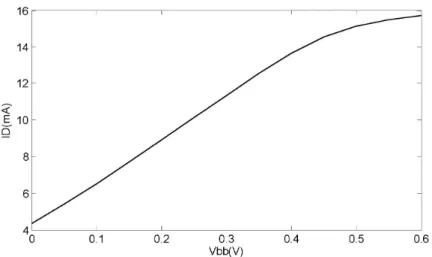
C ∗ |2φ + V | − |2φ | (8) Where V is the threshold voltage when V = 0 V, N is the substrate doping, ε is a physical parameter with a typical value of 0.3 V, and C is the parasitic capacitance at the gate oxide. By applying a forward body bias voltage to the body through a current-limiting resistor R , a forward junction between body and source terminal appears. Therefore, we can adjust V to change V and increase the current flow through the MOSFET [12]. Fig. 2-8 shows the simulated drain current of a NMOS, which has same size and operation condition with the NMOS ~ in the proposed QVCO as shown in Fig. 2-5(a).
16
Fig. 2-9 Drain current of the MOSFET with FBB
In the proposed QVCO as shown in Fig. 2-5(a), bias voltages V is used to the body of each cross-coupled NMOS FETs M , M , M , and M to increase the currents without higher V . After all, we can achieve the operation current with lower V .
17
2.3 Chip Layout and Simulation Results
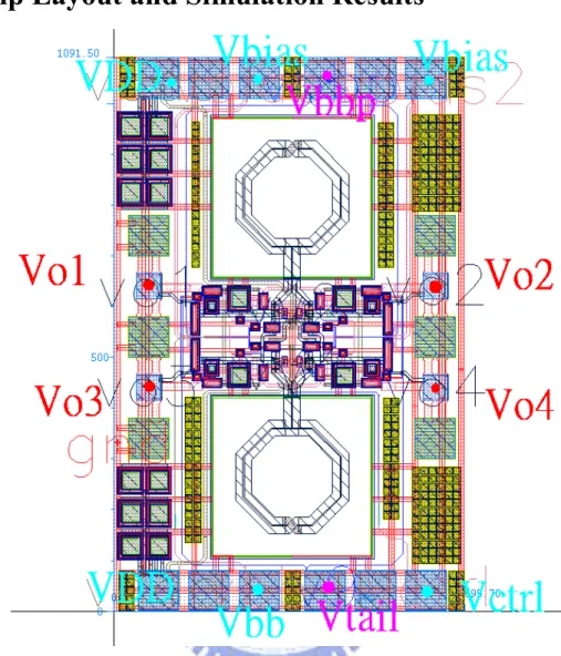
Fig. 2-10 Chip layout of the proposed QVCO
18
Fig. 2-10 shows the chip layout’s photograph of the proposed QVCO, which designed and processed by TSMC 0.18μm mixed-signal/RF CMOS 1P6M technology. The chip area is 0.7*1.1 mm including all pads and bypass capacitances, and each buffer of the quadrature outputs were designed as a common-drain voltage follower. The ADS simulation results is shown in Fig. 2-11, Fig. 2-12, and Fig. 2-13. The oscillating frequency of the QVCO is 5.22 GHz, and the phase noise is-120.1 dBc/Hz @ 1 MHz offset frequency. As the tuning voltage raising from 0 V to 3 V, the tuning range of the QVCO is about 120 MHz from 5.22~5.34 GHz. In Fig. 2-13, the outputs voltage waveform with the peak-to-peak voltage is about 0.87 V, and the phase error < 2 . The QVCO core circuit draws 4.56 mA from a 1.4 V supply.
19
Fig. 2-13 the outputs waveform of the proposed QVCO
To take all performance into account, the figure-of-merit (FOM) is expressed as
(∆ ) = − (∆ ) + 20 (
∆ ) − 10 ( ) (9) where is the oscillating frequency, ∆ is the offset frequency, and is the power
consumption (in mW) of the QVCO. The FOM of the proposed QVCO is about 186 @ 1 MHz offset frequency.
Table 2-2 QVCO simulated performance in different corner condition
corner TT FF SS Tuning Range (GHz) 5.22~5.34GHz 5.13~5.2GHz 5.12~5.17GHz
Phase Noise (dBc/Hz) -120@1MHz -115@1MHz -108@1MHz
20
2.4 Measurement Results and Discussion
2.4.1 Measurement Consideration
The proposed QVCO are designed for on-wafer testing, and the DC voltage are supplied by two sets of six-pin probe, so that the distance between each DC pad must more than 50 μm to satisfy the probe testing rule. The outputs buffer of each quadrature outputs voltage is designed using common-drain voltage follower, and the source end of each buffer MOSFET is connected to a RF pad. For measurement, we connect four bias-tee terminals to the corresponding RF pads as shown in Fig. 2-14.
Fig. 2-14 Bias-Tee model
The phase noise, tuning range and outputs spectrum are measured using signal source analyzer (Agilent E5052A) and down-converter (Agilent E5053A) shown in Fig. 2-15.
(a)SSA(Agilent E5052A) (b)down-converter(Agilent E5053A)
21
2.4.2 Measurement Result
Fig. 2-16 Chip photo of the proposed QVCO
Fig. 2-16 is the chip photograph of the proposed current-shaping QVCO. According to the figures below, this QVCO oscillates at 5.28 GHz and the output power is -5 dBm. The measured phase noise is -119.3 dBc/Hz @ 1 MHz offset frequency, and the tuning range is about 140 MHz since 5.3 GHz ~ 5.44 GHz. Fig. 2-20 also shows the measured outputs voltage waveform, because of the phase delay and loss of the cable line and connector, the phase error is about 7 ~15 . After all, the power consumption of the implemented QVCO is about 11.2 mW, and the FOM is around 183 @ 1 MHz offset frequency.
22
Fig. 2-17 the measured phase noise of the proposed QVCO
23
Fig. 2-19 the tuning range of the proposed QVCO
24
Table 2-3 comparison between simulation and measurement
performance Post-simulation Measurement Supply voltage 1.4 V 1.4 V Tuning range 5.22 ~ 5.34 GHz 5.3 ~ 5.44 GHz Phasenoise@1MHz -120 dBc/Hz -119 dBc/Hz Power consumption 6.384 mW 11.2 mW Output power 0 dBm -5 dBm FOM -186 -183
Table 2-4 comparison between this work and references
performance This work [13] [14]
Oscillation frequency 5.3 GHz 5 GHz 3.6 GHz Phase noise@1MHz -119 dBc/Hz -118 dBc/Hz -114 dBc/Hz Power consumption 11.2 mW 16.5 mW 8 mW FOM -183 -180 -176
25
Chapter 3 Current-Reused QVCO
3.1 Introduction
Recently, due to the demand for the low-power, low-cost, and highly integrated transceiver, many research have focused on the low-power voltage-controlled oscillator (VCO) design. There are various ways to reduce the power consumption of the VCO, and the most common method is reusing the dc currents of the devices[15-17]. In our design, we proposed a current-reused topology to stack the switching transistors of the VCO vertically. Therefore, the dc current drew by the oscillator core can be cut in half of the conventional VCO as sown in Fig. 3-1.
Fig. 3-1 (a) the conventional VCO (b) the current-reused VCO
According to most of the modern wireless communication standards require quadrature modulation, accurate quadrature generations in the VCOs is required. For quadrature signals, in-phase (I) and quadrature-phase (Q) match is an important requirement while meeting the requirements of low-phase noise and low-power for integrated VCOs. The quadrature
26
characteristics can be evaluated in terms of phase error and amplitude imbalance. There are several ways to couple two VCOs in quadrature phase[10, 18]. One common quadrature VCO (QVCO) topology is utilizing the parallel coupling transistors[19], which consumes large current to bias both the switching and coupling transistors. In order to reduce the power consumption, we couple two current-reused VCOs by back-gate coupling technique[20]. We first assume all switching transistors are in different wells, so that each transistor can be used as full four-terminal device. Therefore, the output signals of one VCO can be coupled to the back-gate of the switching transistors of the other VCO. A low-power QVCO without requiring additional coupling transistors can be obtained.
27
3.2 Circuit Design Consideration
A. Current reused differential VCO
Fig. 3-2 the current reused differential VCO
Fig. 3-2 shows the topology of a current reused differential VCO for low-power consumption application[21]. For dc operation, the switching NMOS M and M are stacked vertically, therefore the dc current of M and M can be reused. The resistors R are adopted for diode connection of M and M to ensure M and M are both operating in active region. For constituting a differential VCO in ac operation, the external capacitor C is for ac ground and the capacitors C are adopted for ac coupling. The LC tank of the VCO is composed of L and varactor C . Therefore, a low-power consumption differential VCO can be obtained.
28
B. the proposed current reused QVCO with back-gate coupling
Fig. 3-3(a) the proposed current reused QVCO
29
In Fig. 3-3(a), we proposed a quadrature VCO with the same idea of current reused topology as mentioned before. For reusing the dc current, the switching transistors M and M are stacked vertically, and M and M are stacked vertically, too. The coupling capacitors C are both for ac coupling and dc blocking, therefore, the differential outputs I and I , Q and Q can be generated. Because of the dc voltages at the drain of M , M , M , and M are different, we utilize the resistors R for diode connection to ensure all switching transistors are operating in active region. The LC tank are designed with L and C . Since the dc voltages are different between two differential output nodes, the control voltages of the varactors were supplied as V and V separately. The I and Q signals of the proposed QVCO are generated by coupling two differential VCOs through C to the back-gate of the switching transistors M -M . For back-gate coupling[20], V and V bias the body voltages of M -M for different condition through resistors R , and C is the coupling capacitors to couple the output signals in quadrature phase. The external capacitors C have large value to have tight ground effects for ac currents. Therefore, the power consumption of the proposed QVCO can be cut in half by reusing the dc currents compared to the conventional QVCO topologies.
30
C. back-gate coupling
Fig. 3-4(a) a conventional parallel-coupled QVCO
Fig. 3-4(b) the small signal equivalent circuit of M and M
Fig. 3-4(a) shows a conventional parallel- coupled QVCO (P-QVCO) where the I and Q signals are generated by coupling two differential VCOs through coupling transistors M in parallel with the switching transistors M -M . Because of the differential pair circuits M -M and M -M are symmetric, we use a single-ended analysis to make the analysis simple. Fig. 3-4(b) shows the small signal equivalent circuit of the switching transistor M and corresponding coupling transistor M . The coupling strength α of the P-QVCO can be defined as[22]
31
where is the transconductance and is the width of the coupling transistor M , and and are the transconductance and width of the switching transistor M . The phase noise degradation of the P-QVCO is induced by the increase in transconductance of the coupling transistors. On the other hand, the phase error is reduced while α increasing as the increase in . Therefore, a trade-off between phase noise and phase error occurs. In addition, the coupling transistors lead a higher power consumption of the QVCO.
Fig. 3-3(b) shows the small signal equivalent circuit of the switching transistor M in
Fig 3-3(a). The coupling strength α through the back-gate can be given by[22]
α = = γ
2 2Φ − V (3 − 2) Where is the body effect coefficient, Φ is the work function, and V is the back-gate (body) to source bias voltage. Therefore, we can increase α by minimizing the body-to-source reverse bias V in order to reduce the phase error without additional power consumption.
In our design, by reusing the dc currents of switching transistors, the power consumption of the proposed QVCO shown in Fig. 3-3(a) can be half of the conventional QVCO. Low phase noise and phase error can also be obtained without higher power consumption by back-gate coupling to generate the I and Q signals.
32
3.3 Simulation Results
The ADS simulation results of the proposed current-reused QVCO are shown in Fig. 3-5
~ Fig. 3-8. The proposed QVCO operates at 9.98GHz oscillating frequency, and the phase noise is -112 dBc/Hz @ 1 MHz offset frequency. The total power consumption is 1.64 mW since the QVCO core circuit draws 1.37 mA from a 1.2 V V supply. As the tuning voltages and raising from 0 V to 3 V and 0.6 V to 3.6 V, the tuning range of the QVCO is about 4 GHz from 9.98~13.97 GHz. Fig. 3-7 shows the time domain voltage waveform at the output nodes. Fig. 3-8 shows the output voltages waveform through a dc blocking capacitor, and the phase error of the proposed QVCO < 0.2 . The FOM of the proposed QVCO is about 189.6 @ 1 MHz offset frequency.
33
Fig. 3-6 the simulated tuning range of the proposed QVCO
34
Fig. 3-8 the outputs voltage waveform through dc blocking capacitors
Table 3-1 the comparison between the proposed QVCO and references
This work(sim) [20] [21] Tuning Range (GHz) 9.98~13.97GHz 1.047~1.39GHz 3.0~3.2GHz
Phase Noise (dBc/Hz) -111@1MHz -120@1MHz -102
Core Power 1.64mW 5.4mW 4.32mW
35
Chapter 4 Conclusion
4.1 Simulation Results
In chapter 2, a low-phase noise QVCO utilizing tail current-shaping technique has been proposed. The low-phase noise QVCO is base on two first-harmonic injection-locked oscillators. In order to reduce the phase noise, we inject the output signals of the proposed QVCO back to its tail transistors and shape the tail currents. With this tail current-shaping technique, the RMS value of the impulse sensitivity function (ISF) of the proposed QVCO can be reduce to only 60% of the conventional one. The LC tank of the proposed QVCO has also been designed so as to increase the output amplitude, and the forward-body-bias technique is used to maintain the dc current without higher voltage supply. The measured results are shown in chapter 2.4, the phase noise is -119 dBc/Hz @ 1 MHz offset and the oscillation frequency of the QVCO is 5.28 GHz. The power consumption is 11.2 mW of 1.4 V supply voltage.
In chapter 3, we proposed a low-power QVCO by utilizing a novel current-reused topology. In order to reduce the power consumption, we not only reuse the dc current of the switching transistors, but also couple the quadrature signals by using back-gate coupling technique to avoid using additional coupling transistors. The simulated results are shown in chapter 3.3, the power consumption is only 1.64 mW of 1.2 V voltage supply. The phase noise is -111.7 dBc/Hz @ 1 MHz offset and the oscillation frequency of the QVCO is 10 GHz. The tuning range is from 9.98 GHz to 13.97 GHz, and the figure of merit (FOM) is -189.6 dBc.
36
Reference
[1] IEEE 802.15 WPAN Gigh Rate Alternative PHY Task Group 3a (TG3a).http//www.ieee802.org/15/pub/TG3a.html.
[2] DS-UWB Physical Layer Submission to 802.15 Task Group 3a, [Online]. Available:
ftp://ftp.802wirelessworld.com/15/04/15-04-0137-03-003a-merger2-proposal-ds-uw b-update.doc,available at
[3] Multi-band OFDM Physical Layer Proposal for IEEE 802.15 Task Group 3a, [Online]. Available: ftp://ftp.802wireleesworld.com/15/Archive/2003/Jul03/03268r3P802-15
TG3a-Multi-Band-CFP-Document. doc, available at
[4] A. Hajimiri and T. H. Lee, "A general theory of phase noise in electrical oscillators,"
Ieee Journal of Solid-State Circuits, vol. 33, pp. 179-194, Feb 1998.
[5] K. Kwok and H. C. Luong, "Ultra-low-Voltage high-performance CMOS VCOs using transformer feedback," Solid-State Circuits, IEEE Journal of, vol. 40, pp. 652-660, 2005.
[6] B. Soltanian and P. R. Kinget, "Tail Current-Shaping to Improve Phase Noise in LC Voltage-Controlled Oscillators," Solid-State Circuits, IEEE Journal of, vol. 41, pp. 1792-1802, 2006.
[7] S. L. Jang, S. S. Huang, C. F. Lee, and M. H. Juang, "CMOS Quadrature VCO
Implemented With Two First-Harmonic Injection-Locked Oscillators," Ieee Microwave
and Wireless Components Letters, vol. 18, pp. 695-697, Oct 2008.
[8] P. Andreani and X. Y. Wang, "On the phase-noise and phase-error performances of multiphase LC CMOS VCOs," Ieee Journal of Solid-State Circuits, vol. 39, pp.
1883-1893, Nov 2004.
37
lower phase noise in LC oscillators," in Electronics, Circuits and Systems, 2008. ICECS
2008. 15th IEEE International Conference on, 2008, pp. 392-395.
[10] P. Andreani, A. Bonfanti, L. Romano, and C. Samori, "Analysis and design of a 1.8-GHz CMOS LC quadrature VCO," in IEEE International Solid-State Circuits Conference (ISSCC
2001), San Francisco, California, 2001, pp. 1737-1747.
[11] F. Bahmani and E. Sanchez-Sinencio, "A stable loss control feedback loop for VCO amplitude tuning," Ieee Transactions on Circuits and Systems I-Regular Papers, vol. 53, pp. 2498-2506, Dec 2006.
[12] H. H. Hsieh and L. H. Lu, "A high-performance CMOS voltage-controlled oscillator for ultra-low-voltage operations," Ieee Transactions on Microwave Theory and
Techniques, vol. 55, pp. 467-473, Mar 2007.
[13] S. L. Jang, Y. H. Chuang, S. H. Lee, L. R. Chi, and C. F. Lee, "An Integrated
5–2.5-GHz Direct-Injection Locked Quadrature LC VCO," Microwave and
Wireless Components Letters, IEEE, vol. 17, pp. 142-144, 2007.
[14] L. Shuenn-Yuh and C. Ching-Yi, "Analysis and Design of a Wide-Tuning-Range VCO With Quadrature Outputs," Circuits and Systems II: Express Briefs, IEEE Transactions
on, vol. 55, pp. 1209-1213, 2008.
[15] K. G. Park, C. Y. Jeong, J. W. Park, J. W. Lee, J. G. Jo, and C. Yoo, "Current reusing VCO and divide-by-two frequency divider for quadrature LO generation," Ieee Microwave
and Wireless Components Letters, vol. 18, pp. 413-415, Jun 2008.
[16] S. H. Lee, S. L. Jang, Y. H. Chuang, J. J. Chao, J. F. Lee, and M. H. Juang, "A low power injection locked LC-tank oscillator with current reused topology," Ieee Microwave and
Wireless Components Letters, vol. 17, pp. 220-222, Mar 2007.
[17] Y. H. Chuang, S. L. Jang, S. H. Lee, R. H. Yen, and J. J. Jhao, "5-GHz low power current-reused balanced CMOS differential Armstrong VCOs," Ieee Microwave and
38
[18] X. Y. Li, S. Shekhar, and D. J. Allstot, "G(m)-boosted common-gate LNA and differential colpitts VCO/QVCO in 0.18-mu m CMOS," in IEEE International Solid-State Circuits
Conference (ISSCC 2005), San Francisco, CA, 2005, pp. 2609-2619.
[19] S. B. Shin, F. C. Choi, and S. G. Lee, "Source-injection parallel coupled LC-QVCO,"
Electronics Letters, vol. 39, pp. 1059-1060, Jul 2003.
[20] H. R. Kim, C. Y. Cha, S. M. Oh, M. S. Yang, and S. G. Lee, "A very low-power quadrature VCO with back-gate coupling," Ieee Journal of Solid-State Circuits, vol. 39, pp. 952-955, Jun 2004.
[21] N. J. Oh and S. G. Lee, "Current reused LC VCOs," Ieee Microwave and Wireless
Components Letters, vol. 15, pp. 736-738, Nov 2005.
[22] J. P. Hong, S. J. Yun, N. J. Oh, and S. G. Lee, "A 2.2-mW backgate coupled LC quadrature VCO with current reused structure," Ieee Microwave and Wireless