國 立 交 通 大 學
電子工程學系 電子研究所碩士班
碩 士 論 文
互補式金氧半八位元 50MHz 取樣頻率管線化
類比至數位轉換器之設計與分析
The Design and Analysis of a CMOS 8bit
50MS/s Pipelined Analog-to-Digital
Converter
研 究 生 : 夏志朋
指導教授 : 吳錦川 教授
互補式金氧半八位元 50MHz 取樣頻率管線化
類比至數位轉化器之設計與分析
The Design and Analysis of a CMOS 8 bit
50MS/s Pipelined Analog-to-Digital Converter
研究生:夏志朋 Student:Chih-Peng Hsia
指導教授:吳錦川 教授 Advisor:Prof. Jiin-Chuan Wu
國立交通大學
電子工程學系 電子研究所碩士班
碩士論文
A Thesis
Submitted to Department of Electronics Engineering & Institute of
Electronics
College of Electrical Engineering and Computer Science
National Chiao Tung University
In Partial Fulfillment of the Requirements
for the Degree of
Master of Science
In
Electronic Engineering
Sep 2005
Hsin-Chu, Taiwan, Republic of China
互補式金氧半八位元 50MHz 取樣頻率管線化
類比至數位轉化器之設計與分析
學生: 夏 志 朋 指導教授: 吳 錦 川 博士
國立交通大學
電子工程學系 電子研究所碩士班
摘要
本論文研究工作電壓 3.3 伏特, 8 位元,每秒 50 百萬次取樣頻率之管線 化類比至數位轉換器( ADC ) ,並以台積電 0.35um 2P4M 互補式金氧半製程模 擬與設計。本設計採用每級 1.5 位元與其數位錯誤修正技術來降低功率消耗與 提升速度。主要元件如下:餘數放大器( residue amplifier ),比較器( dynamic comparator ) ,正反器 ( flip-flop ) ,加法器( adder ) 與時脈產生器( clock generator ) 。整個電路是以每級 1.5 位元共六級與最後一級 2 位元,再加上一 個前端輸入保持電路所組成。並在輸入端使用拔靴帶電路提高取樣訊號的線性 度;輸入信號為全差動正負一伏特信號。此類比至數位轉換器在操作時脈為每秒 50百萬次時共消耗146mW。微分和積分非線性誤差在Matlab模擬別為±0.25LSB 和±0.5LSB。The Design and Analysis of a CMOS 8 bit
50MS/s Pipelined Analog-to-Digital
Converter
Student: Chih-Peng Hsia Advisor: Prof. Jiin-Chuan Wu
Department of Electronics Engineering & Institute of Electronics
National Chiao-Tung University
ABSTRACT
The thesis describes the design of a 3.3 V, 8-bit, 50M sample/s CMOS pipelined analog-to-digital converter (ADC) implemented by simulation with 0.35um double-poly four-metal process. The component in the ADC is the residue amplifier, the dynamic comparator, the flip-flop, the adder and the clock generator. The prototype ADC is implemented by an input sample-and-hold circuit (S/H), 6 identical 1.5-bit stages and a 2-bit final stage. Bootstrapping switch is needed to provide the linearity in the front-end S/H. The 1.5b/stage architecture with digital error correction is used in this ADC for low-power and high-speed considerations. The input signal is fully differential; the input range is ±1 V. The ADC converter dissipates 146mW at a 50MHz clock rate with 3.3 V single supply voltage. Typical differential nonlinearity (DNL) is ±0.25LSB and integral nonlinearity (INL) is ±0.5LSB by MATLAB simulation.
誌謝
回顧這兩年的研究生涯,總總事物似乎皆是在一瞬間所發生,求學與生活壓 力令我幾乎喘不過氣來,對於生活週遭的事物不再敏銳,甚至迷惘;如果沒有朋 友們的鼓勵,這樣的無力感或許已經令我放棄學業;沒有吳錦川老師的教導,我 或許就走錯了方向;所以在此,我首先是要感謝吳錦川老師,老師對學生的態度 不只像是師生,更像是對待自己的小孩一般,老師不只在繁忙之餘給我們研究上 指點,並在平常的聊天中給我們生活上的一些經驗,我相信這將比專業上的心得 影響我們更多更久。也要感謝陳巍仁教授、邱煥凱教授與張恆祥學長撥冗擔任我 的口試委員,並且提供我研究上不少寶貴的意見與經驗,使我受益良多。 接下來我要感謝我的父母,只因為有他們全心全力的支持,才能讓我順利完 成在研究所這兩年來的課業與目標,這份論文才能順利地完成。還要感謝 307 實 驗室的學長不吝嗇地將經驗傳承下來,還要感謝 527 一起打拼的夥伴,小鍵、諭 哥、傑忠、POLO、巴嘿、粘哥、袋鼠、紅毛、建樺、弼嘉、台祐、黃忠西等好多 好多人,有了你們,平淡的研究生活才多了許多樂趣,要感謝的人還有很多,在 此一併感謝。 最後要感謝我的女朋友文瑛,總是給予我最大的支持與鼓勵,只因為有妳, 我才能全心的研究,只因為有妳,我才能頂住最後的壓力,真的是辛苦妳了。 謹以此篇論文獻給所有關心我的人。 夏志朋 國立交通大學 中華民國九十四年九月CONTENTS
CHINESE ABSTRACT I
ENGLISH ABSTRACT II
ACKNOWLEDGEMENT III
CONTENTS IV
TABLE CAPTIONS VII
FIGURE CAPTIONS VIII
CHAPTER 1 Introduction
1.1 Motivation 1 1.2 Thesis Organization 2CHAPTER 2 Fundamentals
2.1 Introduction 3 2.2 ADC Performance 3 2.2.1 Dynamic Performance 32.2.1.1 Signal-to-Noise Ratio, Effective Number of Bits 4 2.2.1.2 Signal to Noise plus Distortion Ratio 6 2.2.1.3 Spurious-Free Dynamic Range 7 2.2.1.4 Fast Fourier Transform Test 8
2.2.2 Static Performance 9
2.3 Reviews of ADC Architecture 10
2.3.1 Flash ADC 11
2.3.2 Successive Approximation Register ADC 13
2.3.4 Pipelined ADC 15
2.3.4.1 Pipelined ADC versus Flash ADC 16 2.3.4.2 Pipelined ADC versus SAR ADC 16
2.3.4.3 Pipelined ADC versus Over-sampling ADC 17
2.4 Summary 17
Chapter 3 General Considerations
3.1 Introduction 18
3.2 1.5bit/Stage Pipelined ADC Architecture 18 3.2.1 The Stage Resolution with Power Consideration 20 3.2.2 The Stage Resolution with Speed Consideration 23
3.3 Digital Error Correction 24
3.4 Non-ideal Considerations and Stage Requirement 30 3.4.1 Residue Amplifier Gain Error 30 3.4.2 Finite Settling Time of Op-amp 32 3.4.3 Capacitor Mismatch and Size 33
3.4.4 Aperture Uncertainty 34
Chapter 4 Circuit Design
4.1 Architecture of the ADC 36
4.2 Sample-and-hold 37
4.2.1 Switches 39
4.2.2 Bootstrapped switch 40
4.2.3 Op-amp 41
4.2.4 CMFB 43
4.2.5 Op-amp Bias Circuit 44
4.2.7 Simulation Result of S/H 47
4.3 Multiplying DAC 49
4.3.1 Comparator 50
4.3.2 MDAC Simulation Result 52
4.4 Digital Error Correction & Clock Generator 54 4.5 Simulated Result of Pipelined ADC 56 4.6 Simulated Result of Pipelined ADC with Power Noise 59
Chapter 5 Conclusions
5.1 Conclusion 62
RENFERENCES 64
TABLE CAPTIONS
Table 2.1 Coarse list of ADC architectures ... 11
Table 4.1 switches type and size for S/H... 40
Table 4.2 Transistor size of telescopic op-amp ... 43
Table 4.3 Transistor size of bias circuit ... 45
Table 4.4 The minimum requirement of the op-amp... 46
Table 4.5 switches type and size for MDAC... 50
Table 4.6 (a) transistor size in comparator for decision level is 0.25*Vref ...51
FIGURE CAPTIONS
Figure 1.1 A/D interface between the external world and digital system... 2
Figure 2.1 Transfer diagram for ideal linear ADC and quantization error of an ADC ... 5
Figure 2.2 The probability density function of the quantization error ... 5
Figure 2.3 Typical SNDR versus signal level for an ADC... 7
Figure 2.4 Magnitude spectrum of a quantized sine wave. Data record size N = 1024 ... 8
Figure 2.5 Transfer characteristic of ADC showing INL and DNL ... 10
Figure 2.6 Flash ADC Architecture... 11
Figure 2.7 Thermometer code is similar as a mercury thermometer ... 12
Figure 2.8 D/A converter-based successive-approximation converter... 13
Figure 2.9 Delta-Sigma architecture ... 14
Figure 2.10 Pipelined architecture ... 15
Figure 3.1 B-bit/stage pipelined ADC topology ... 19
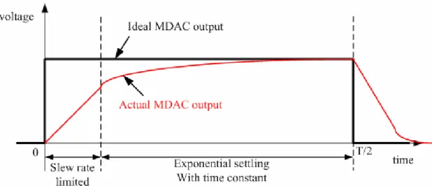
Figure 3.2 Settling of the MDAC output ... 21
Figure 3.3 A single-ended MDAC ... 21
Figure 3.4 the normalized total current for different stage resolution ... 23
Figure 3.5 the particular MDAC output... 24
Figure 3.6 (a) Ideal transfer curve of a 2/stage with (b) Gain error (c) Comparator offset... 25
Figure 3.7 The modify 2bit/stage transfer curve ... 26
Figure 3.8 2 bit redundant sign digital correction ... 27
Figure 3.10 the effect of comparator offsets for the pipelined ADC
with (a) offset=0 (ideal) (b) offset=0.2 Vref (c) offset=0.3 Vref ...28
Figure 3.11 INL of the pipelined ADC with comparator offset = (a) 0.2 Vref (b) 0.3 Vref ...29
Figure 3.12 the MDAC operation ... 31
Figure 3.13 Aperture uncertainty ... 35
Figure 4.1 pipelined architecture used in this design and timing strategy ... 36
Figure 4.2 Schematic diagram of Flip-Around sample-and-hold ... 37
Figure 4.3 the S/H operation ... 38
Figure 4.4 Switch in sampling mode... 39
Figure 4.5 Clock bootstrapped switch (a) Conceptual schematic (b) circuit implementation... 40
Figure 4.6 Simulation result of the clock bootstrapped switch ... 41
Figure 4.7 Telescopic op-amp ... 42
Figure 4.8 Switch capacitor CMFB circuit ... 43
Figure 4.9 Telescopic op-amp with bias circuit ... 45
Figure 4.10 SC-CMFB AC simulation model... 46
Figure 4.11 Simulated frequency response of the op-amp ... 47
Figure 4.12 Simulation result of S/H (a) transient response (b) FFT spectrum ... 48
Figure 4.13 Schematic diagram of Multiplying DAC... 49
Figure 4.14 (a) Dynamic comparator... 51
Figure 4.14 (b) Dynamic comparator with decision level 0... 52
Figure 4.15 (a) MDAC control logic for each stage (b) MDAC output logic for the terminal stage... 53
Figure 4.16 Simulation result of MDAC transient response... 54
Figure 4.18 Schematic of the clock generator... 55
Figure 4.19 (a) Timing diagram (b) the simulation of clocks ... 56
Figure 4.20 Simulated results of the pipelined ADC (a) Transient response (b) DNL (c) INL... 57
Figure 4.21 512 points FFT spectrum of the pipelined ADC at 24.8046875MHz input signal... 58
Figure 4.22 512 points FFT spectrum of the pipelined ADC at 2.24609375MHz input signal... 58
Figure 4.23 SNDR and SFDR versus input frequency ... 59
Figure 4.24 The simulated power PAD ... 60
Figure 4.25 Power noise... 60
Figure 4.26 Simulated results of the pipelined ADC with power noise (a) DNL (b) INL... 60
Figure 4.27 512 points FFT spectrum of the pipelined ADC at 292.96875KHz input signal ... 61
1
Introduction
1.1 Motivation
The CMOS technology has dominated the mainstream silicon IC industry in the last decades. The evolution of CMOS technology into the deep-submicron region has made possible the integration of more digital signal processing (DSP) system on a single VLSI chip. Therefore, more and more signal processing functions are implemented for a lower cost and lower power consumption with the fast advancement of CMOS fabrication technology. Digital circuits have achieved high speed and low power dissipation. With this trend, most analog circuits are replaced by digital circuits in a mixed signal circuits. However, the interfaces of the system to the external world will still remain in the analog signal domain, illustrated in Figure 1.1, convert the continuous-time signals to discrete-time, binary-coded form. Thus an analog-to-digital interface is the limits of the speed and accuracy in the systems that operate on a wide variety of continuous-time signals, such as speech, medical imaging, sonar, radar, electronic warfare, instrumentation, consumer electronics, and telecommunications [1]. The speed of ADC must scale with the speed of the digital circuits in order to fully utilize the advantages of advanced DSP technologies.
Figure 1.1 A/D interface between the external world and digital system [2] As the CMOS processing improved, the MOS device has kept shrinking minimum feature size and greatly impacted the performance of digital circuits. The increasing integration level for integrated circuits has forced the ADC interface to reside on the same silicon with large DSP and digital circuits for lower cost. The noise immunity of ADC has become an important issue of sharing the substrate of analog circuits with noisy digital logic gates. And the lower power supply voltage is a great challenge to design high performance ADC [3].
The goal of this research is to examine the nonlinearity error source in ADC and to develop a high-speed medium-resolution analog-to-digital converter (ADC) in standard CMOS technology. Such ADC find wide applications in battery powered instruments and low cost digital oscilloscopes.
1.2 Thesis Organization
This thesis is organized into five chapters. In Chapter 1, this thesis is briefly introduced.
Chapter 2 begins with performance metrics used to characterize ADCs. Then several ADC are reviewed and compared with pipelined ADC. In Chapter 3, the 1.5-bit architecture with digital error correction is presented. In Chapter 4, the design and analysis of circuits in each building block will be described. In Chapter 5, the conclusion and perspectives are presented.
2
Fundamentals
2.1 Introduction
In this chapter, we describe the metrics of ADC which is commonly used in measurement at first. The second is a survey of ADC architectures and comparison with pipelined ADC. Some converters are suitable for high resolution and some are used for high-speed application. Here, we will briefly discuss operation and characteristic of these architectures as follows.
2.2 ADC Performance
In order to character the ADC performance, some performance metrics and method are used widely. They can be divided into the static and the dynamic performance. ADC is characterized in a number of different ways to indicate this performance capability and nonlinearity error. Some of the most important performance metrics of ADC are introduced as below.
2.2.1 Dynamic Performance
Frequency-domain test for ADC’s are widely employed and allow a quick analysis of the dynamic performances of an ADC. Resolution describes the finite
number of the quantization that the ADC can produce. It can be expressed in bits as digital data or in volts electrically. An n-bit resolution implies that ADC can resolve 2n distinct digital levels. The resolution is not necessarily an indication of the accuracy of the converter, but instead it refers to the number of digital output bits. For example, an 8bit ADC which has 256 level outputs only can determine 128 level inputs. We can say the real resolution of the ADC only is 7bit. Therefore, most techniques for characterizing the real resolution of an ADC are to measure either noise, nonlinearity, or both.
2.2.1.1 Signal-to-Noise Ratio, Effective Number of Bits
Sometimes the real resolution is called as effective number of bits (ENOB). It usually defined with the signal-to-noise ratio (SNR). SNR is the ratio of the root-mean-square (rms) signal amplitude to the square-root of the integral of the noise power spectrum over the frequency band of interest. For a Nyquist rate converter the frequency band of interest ranges is from 0 to the half of sample rate. The noise spectrum contains contributions from all the error mechanisms present. These include quantization noise, circuit noise, aperture uncertainty, and comparator ambiguity [1].
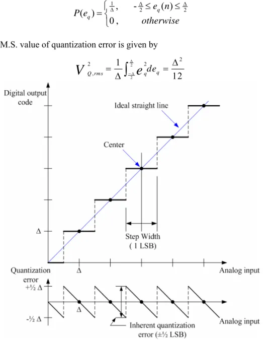
The quantization noise due to the finite quantization level defined as the difference between the input signal and the ADC output signal. It ranges between plus or minus half least-significant-bit (LSB), as shown in Figure 2.1. Furthermore, the quantization error can be considered as a noise if all quantization level is exercised with equal probability, the quantization steps are uniform, as shown in Figure 2.2
The quantization error (eq) is uniformly distributed from –Δ/2 to +Δ/2. And the
probability function P(eq) for such error signals is a constant value. Therefore, the
equation of the quantization error is expressed as Equation (1), is similar to white noise.
1 2 2 , - ( ) ( ) , 0 q q e n P e otherwise Δ Δ Δ ≤ ≤ ⎧ = ⎨ ⎩ (1)
The R.M.S. value of quantization error is given by
2 2 2 2 2 , 1 12 q Q rms qde
V
e
Δ − Δ Δ = = Δ∫
(2)Figure 2.1 Transfer diagram for ideal linear ADC and quantization error of an ADC
Figure 2.2 The probability density function of the quantization error
In general, when the quantization noise signal is uniformly distributed over the interval ±VLSB/2, the R.M.S. quantization noise voltage equals VLSB/ 12 and is
independent of the signal frequency. In measurement, a pure sinusoidal waveform usually use as input signal which is between reference voltages, ±Vref. Thus, the
R.M.S. value of the sinusoidal wave is
sin, 2
ref rms
V
V
= (3)Hence, the voltage of the least-significant-bit in N bits ADC has relationship with Vref
and the number of bits.
2 2 ref N LSB V
V
= Δ = (4)Then the SNR of the full-scale sinusoidal wave is given by
, 10 , 10 10 20log 3 2 20log 20log 2 2 12 input rms Q rms ref N LSB V Signal Power SNR
Total Noise Power V V V ⎛ ⎞ = = ⎜⎜ ⎟⎟ ⎝ ⎠ ⎛ ⎞ = = ⎜⎜ ⎟⎟ ⎝ ⎠ (5)
It can also be expressed in dB:
SNR=6.02N+1.76 dB
(6)The equation (6) shows the best possible SNR for an N-bit ADC with sinusoidal wave input. However, the idealized SNR decreases from the best possible value for reduced input signal levels [4] [5] [6].
2.2.1.2 Signal to Noise plus Distortion Ratio
The signal to noise plus distortion (SNDR) is used to measure the degradation due to the combined effect of noise, quantization, and harmonic distortion. The SNDR often measured with a sinusoidal input of Fast Fourier Transform test (FFT). When a sinusoidal signal of a single frequency is applied to a system, the output of the system generally contains a signal component at the input frequency. Because of distortion, the output also contains signal components at harmonics of the input frequency. An
ADC usually samples an input signal at some finite rate. As a result, some of the harmonic distortion products are aliased down to lower frequencies. Furthermore, the ADC adds noise to the output, and this noise generally present to some degree at all frequencies. The SNDR of the ADC is defined as the ratio of the signal power in the fundamental to the sum of the power in all of the harmonics, all of the aliased harmonics, and all of the noise [6].
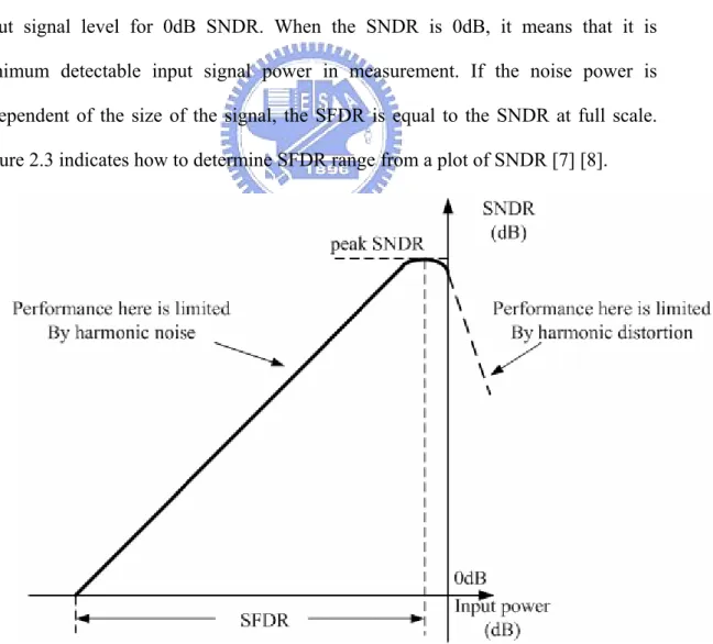
2.2.1.3 Spurious-Free Dynamic Range
Spurious-Free Dynamic Range (SFDR) is the signal-to-noise ratio when the power of the third-order inter-modulation products equals the noise power. Another way to define SFDR is the ratio of the input signal level for maximum SNDR to the input signal level for 0dB SNDR. When the SNDR is 0dB, it means that it is minimum detectable input signal power in measurement. If the noise power is independent of the size of the signal, the SFDR is equal to the SNDR at full scale. Figure 2.3 indicates how to determine SFDR range from a plot of SNDR [7] [8].
2.2.1.4 Fast Fourier Transform Test
It is possible with Fast Fourier Transform techniques to detect the SNR and SNDR of a practical ADC. Using the Fast-Fourier transform (FFT) is one of the most popular ways to convert a series of digital samples from the time domain to the frequency domain. The result of a FFT looks like the output of a spectrum analyzer, shown as Figure 2.4. The FFT assumes that the spectrum does not change over time. The FFT usually produce the average of a signal's frequency content over the time interval that the signal was acquired. Thus, the FFT are always recommended for stationary-signal analysis. Furthermore, if the input signal is not synchronized to the ADC's sampling clock, the spectrum will become smeared, obscuring detail. A spectrum of the FFT result can give the signal peak power and total noise power to calculate SNR.
Figure 2.4 Magnitude spectrum of a quantized sine wave. Data record size N = 1024 In order to speed up the FFT process, we usually sample at least 2N data of the
ADC result to calculate performance. And the input frequency and sampling frequency have the following relation in an experiment:
fin fs 2N
M
= (7)
Where fin is the frequency of input signal and fs is the sampling rate. M is a prime number. It gives that the ratio of the input frequency to the sampling frequency should be the ratio of two relatively prime numbers. It is important to choose the number of 2N that is bigger than the number of ADC quantization levels. Then the harmonic distortion is obvious by decreasing the noise floor [9] [10].
2.2.2 Static Performance
The static linearity is characterized by differential non-linearity (DNL) and integral non-linearity (INL). The input-output characteristic of the ADC approximates a straight line as the resolution increases. The ideal transfer characteristic progresses from low to high in a series of uniform steps. The transfer characteristic of a real ADC contains steps which are not perfectly uniform. DNL and INL are used to characterize this deviation. DNL measures how far each of the step sizes deviates from the ideal value of the step size. INL is the difference between the actual transfer curve and the ideal straight line which ADC is intended to approximate. Figure 2.5 illustrates DNL and INL, which can be expressed as Equation (7) and (8). DNL and INL can be expressed in LSB of the converter input which is equal to the full scale input range of the ADC divided by the number of output levels. Obviously, because we assumed uniform quantization error over ±Δ/2, non-zero DNL across many codes can easily cost a few dB in SNR [2] [11].
LSB
TP(i+1)-TP(i) DNL(i)= 1 ;
ideal LSB
TP(i)-TP(i) INL(i)= ;
V (9)
DNL and INL are usually measured by code density test. Code density analysis requires sampling a large number of times the input sine wave, taking care to cover with uniform probability all the possible phase value in [0, 2π ] [12]. In simulation, we can find all code boundaries by using a ramp signal as input. It can reduce a lot of simulation time when we need to calculate INL and DNL approximately.
Figure 2.5 Transfer characteristic of ADC showing INL and DNL
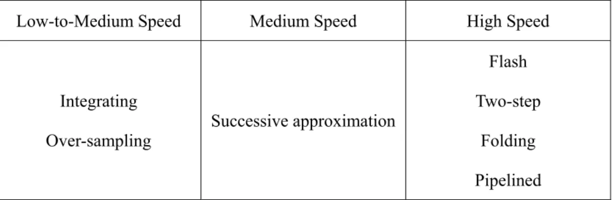
2.3 Reviews of ADC Architecture
Architectures for realizing analog-to-digital converters can be roughly divided into three categories (Table 2.1) --- low-to-medium speed, medium speed, and high speed. In this section, some of the notable architectural styles are introduced and
compared. Each of architecture has advantages and disadvantages, and each has a set of applications for which it is the best solution. We briefly discuss operation and characteristics of flash, pipelined, successive approximation and over-sampling ADC as follows [13].
Low-to-Medium Speed Medium Speed High Speed
Integrating Over-sampling Successive approximation Flash Two-step Folding Pipelined Table 2.1 Coarse list of ADC architectures
2.3.1 Flash ADC
Figure 2.6 Flash ADC Architecture
The architecture is fully parallel to transform data directly. They are suitable for applications requiring very large bandwidths and no latency. Flash ADCs are made by cascading high-speed comparators. Each comparator represents 1 LSB, and the output code can be determined in one cycle. Therefore, an n-bit flash ADC consists of an array of 2N-1 comparators with 2N-1 threshold values. The threshold levels are usually generated by a resistive divider. The set of comparators outputs is often referred to as a thermometer code, so named because it is similar to a mercury thermometer, shown as Figure 2.7. Each comparator produces a "1" when its analog input voltage is higher than the reference voltage applied to it. Otherwise, the comparator output is "0". The level of the boundary between ones and zeros indicate the values of the input signal, as the level of mercury in a mercury thermometer indicates the temperature. Then the thermometer code is decoded to the appropriate digital output code.
Figure 2.7 Thermometer code is similar as a mercury thermometer
The main drawback of flash ADC is the comparators. An n-bit flash ADC required 2N-1 comparators to convert the input data directly. It suffers from this dependence of comparator counts on resolution. The parasitical input capacitance is
increased exponentially when the resolution increases. However, a precise comparator is hard to design in higher resolution. Because of this drawback, flash converters usually consume a lot of power, have low resolution, and can be quite expensive. This limits them to high frequency applications that typically cannot addressed any outer way. Examples include data acquisition, satellite communication, radar processing and high-density disk drives.
2.3.2 Successive Approximation Register ADC
Successive-approximation-register (SAR) ADC is the architecture of the choice for medium-to-high-resolution applications with medium sampling rates. In a SAR converter, the bits are decided by a single high-speed, high-accuracy comparator one bit at a time (from the MSB down to the LSB), by comparing the analog input with a digital-to-analog converter (DAC) whose output is updated by previously decided bits and thus successively approximates the analog input. This serial nature of the SAR limits its speed to no more than a few Msps. SAR ADC is available in resolutions up to 16-bits. It provides low power consumption and high space-efficient.
Figure 2.8 D/A converter-based successive-approximation converter A DAC-based SAR is shown in Figure 2.8. The SAR ADC’s limit often is the settling time of the DAC. A capacitive DAC usually use in the SAR ADC. However, this DAC needs a lot of settling time of the DAC output settling. In addition, the linearity of the overall ADC is limited by the linearity of the DAC. Therefore, SAR ADCs with more than 12 bits of resolution will often require calibration to achieve the
necessary linearity. One feature of SAR ADCs is that power dissipation scales with the sample rate. This is especially useful in low-power applications or applications where the data acquisition is not continuous.
2.3.3 Over-sampling ADC
Figure 2.9 Delta-Sigma architecture
Delta-Sigma ADC is an over-sampling ADC. It is based on the principle of highly over-sampling the input signal followed by a digital filter/decimator to obtain the digital code equivalent, shown as Figure 2.9. The techniques of over-sampling and noise shaping allow the use of relatively imprecise analog circuits to perform high resolution conversion using only a 1 bit ADC. Delta-Sigma ADC is ideal for low bandwidth signals and is capable of very high resolution. Accuracy depends on the noise and linearity performance of the modulator, which uses high performance amplifiers. The converter technology allows for trade-off between signal bandwidth and resolution that is often externally programmable. A digital filter can have greater complexity than its analog equivalent at lower cost, and it is always exactly reproducible over temperature and time. Complex filter functions are readily achieved and are often tailored to a specific application. Applications for Delta-Sigma ADC include industrial process control, analytical and test instrumentation, medical image and acquisition. DSP compatibility makes them ideal choices for system solutions.
2.3.4 Pipelined ADC
The concept of the pipelined ADC is just like the multiplexingpipeline in DSP system, has improve the throughput rate. Figure 2.10 shows the structure of a pipelined ADC. A pipelined ADC improves the throughput rate by using similar multi-stages. The multi-stages convert data sequentially and the result output as there is only one stage. But the conversion time of the pipelined ADC is increased as more as the number of the stages is increased. In other words latency is associated with pipelined systems, and this latency is equal to the number of stages in the pipeline multiplied by the time required to execute the slowest stage.
Figure 2.10 Pipelined architecture
Another feature of the pipelined ADC is that the resolution requirement of the following stages can be relaxed. But the adding stages require more power dissipation in the ADC. However, the pipelined ADCs can achieve high resolutions with relatively little hardware. Furthermore, the comparator offset can be easily eliminated as a limitation to resolution with self calibration techniques. Because of their tolerance to comparator offsets and the ability of the pipelined stages to operate in parallel,
pipelined ADCs are well suited for high resolution applications where high speed is required, just like CCD-based imaging systems, ultrasonic medical imaging and digital receiver.
2.3.4.1 Pipelined ADC versus Flash ADC
Despite the inherent parallelism, a pipelined ADC still requires accurate analog amplification in sub-DACs and inter-stage gain amplifiers, and thus significant linear settling time. A purely flash ADC has a large bank of comparators, each consisting of wideband, low-gain preamps followed by a latch. The preamps, unlike those amplifiers in a pipelined ADC, need to provide gains that don't have to be linear or accurate required; only the comparators' trip points have to be accurate. As a result, a pipelined ADC cannot match the speed of a well-designed flash ADC. But the number of the comparator in flash ADC is increasing exponentially as the resolution increase. Therefore, at sampling rates obtainable by both a pipeline and a flash, a pipelined ADC tends to have much lower power consumption than a flash. A pipelined ADC also tends to be less susceptible to comparator meta-stability. Comparator meta-stability in a flash can lead to errors.
2.3.4.2 Pipelined ADC versus SAR ADC
In a successive approximation register (SAR) ADC, the bit is decided by a single high-speed, high-accuracy comparator bit by bit, from the MSB down to the LSB, by comparing the analog input with a DAC whose output is updated by previously decided bits and successively approximates the analog input. This serial nature of SAR limits its operating speed to no more than a few MS/s, and still slower for very high resolutions. A pipelined ADC employs a parallel structure in which each stage works on 1 to a few bits concurrently. Although there is only one comparator in a SAR, this comparator has to be fast and as accurate as the ADC itself. In contrast, the requirement of the comparator in a pipelined ADC is more relaxed.
2.3.4.3 Pipelined ADC versus Over-sampling ADC
Over-sampling converters trade speed for resolution. The need to sample many times for producing one final result causes the internal analog components in the sigma-delta modulator to operate much faster than the final data rate. The digital decimation filter is also nontrivial to design and takes up a lot of silicon area. The fastest, high-resolution sigma-delta-type converters are not expected to have more than a few MHz of bandwidth in the near future. Like pipelined ADCs, sigma-delta converters also have latency. [13] [14]
2.4 Summary
The pipelined ADC is the architecture of choice for sampling rates from a few MS/s up to 125MS/s. Complexity goes up only linearly with the number of bits, providing converters with high speed, high resolution, and low power at the same time. They are very useful for a wide range of applications, most notably in the digital communication area, where a converter’s dynamic performance is often more important than traditional static specifications like differential nonlinearity and integral nonlinearity. And their data latency is of little concern in most applications.
3
General Considerations
3.1 Introduction
In this chapter, the briefly operational principle of 1.5bit/stage pipelined analog to digital converters is presented. The switched-capacitor circuits usually use in a pipelined ADC design. Here, sources of error in pipelined ADC and error correction techniques are discussed.
3.2 1.5bit/Stage Pipelined ADC Architecture
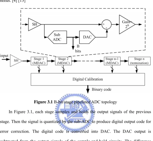
A pipelined ADC consists of a number of identical pipelined stages, as shown in Fig 3.1. It is similar as Figure 2.10, but here we add S/H block and the termination block. The beginning S/H block can relax the timing requirements of the first stage. Following the S/H, it consists of a cascade of N-1 identical stage. Each stage consists of a sample-and-hold amplifier, a digital-to-Analog converter, a low resolution Analog-to-Digital sub-converter, a subtraction, and a fix-gain amplifier. All of the pipelined stages are similar in structure and the functions in block usually are implemented in switched-capacitor circuits. The function of the digital-to-analog converter, the subtraction and the fix-gain amplification are combined into one single circuit called the multiplying DAC (MDAC). The last termination stage is the coarse
ADC. It resolves these LSB used for digital error correction of comparator offset if it needs. [4] [13]
Figure 3.1 B-bit/stage pipelined ADC topology
In Figure 3.1, each stage samples and holds the output signals of the previous stage. Then the signal is quantized by the sub-ADC to produce digital output code for error correction. The digital code is converted into DAC. The DAC output is subtracted from the output signals of the sample-and-hold circuits. The difference signal represents the residue. The redundancy is amplified by 2B to full scale and the output would sample and hold at the next stage.
The sample-and-hold function in each stage allows all stages to operate concurrently. It can hold the input voltage at each stage and relax the conversion time of the comparator. While S/H samples the analog input, the even stages sample the held analog residues from the odd stages hold. At the next phase, the state of the odd stages and the even stages is exchanged. Therefore, the pipelined ADC needs the least two phase clock. The fully resolved n*B bits of resolution pre sample experiences a delay n/2 clock cycle from the analog input to full quantization in Figure 3.1. So the
pipelined ADC is inappropriate for applications that the latency is not acceptable. The conceptual circuit usually is implemented by switched-capacitor technique. The functions are easily realized in transferring the charge from one capacitor to another ratio capacitor. A switched-capacitor circuit is realized with the use of some basic building blocks such as op-amps, capacitors, switches, and non-overlapping clocks. Each block need to consider with speed and accuracy requirement. The first one is deciding the number of bits (B) per stage. For example, to attain maximum throughput rate, we need to reduce the inter-stage gain and increase the corresponding bandwidth of the gain. So the resolution per stage should be small. Therefore, it requires more pipelined stages than large resolution pre stage.
3.2.1 The Stage Resolution with Power Consideration
In pipelined ADC, the most of the power dissipation is the static power of the analog circuit components. The dominated one is the power of the op-amps DC bias current. The current consumption of an operational amplifier is a nonlinear function of the bandwidth. But we can use the approximate square-law transistor current equations to find the optimal stage resolution in the pipelined ADC.
The single pipelined ADC often needs two clock phase. It gives a settling time of a half of the clock cycle. The settling time is determined by the bandwidth and slew rate of the amplifier, as shown in Figure 3.2. MDAC is the most important blocks in the pipelined ADC. Figure 3.3 (a) shows the simply MDAC topology in hold mode as single-ended for simple calculations. All the calculations are performed for a fully differential topology. And the corresponding small-signal model as a single-pole system is presented in Figure 3.3 (b). In Figure 3.3, the input signal is sampled by the sample capacitor Cs and feedback capacitor Cf. and Cp is the parasitic capacitance of op-amp. The CL consists of the total output loading capacitance and the parasitic
Figure 3.2 Settling of the MDAC output
Figure 3.3 A single-ended MDAC
(a) in the hold mode and (b) the corresponding small-signal mode.
We assume the speed of the MDAC circuit is only limited by the time constant in the single pole system. And the slew rate limitation is not considered for simple calculations. We can get the relationship between the input signal and the output signal by Equation (11).
/
(1 t )
out in
V =V −e− τ (11)
Because the signal needs to settle in a half clock cycle, the settling error voltage must be less than 1/2 LSB in the period of time 1/(2fs). (fs: sampling rate) Therefore, we can get Equation (12) with N bit accuracy and the maximum output voltage Vfull-swing.
-1
2
full swing out in NV
V
≥
V
−
+ (12)By combining Equation (11) and (12), and solving the maximum time constant in the worst case (the input voltage is the maximum) yields
1
2
fs N
(
1) ln 2
τ
=
⋅
+ ⋅
(13)The time constant of the MDAC in Figure 3.3(b) is given by
, ,
2
B L total L total m mC
C
g
f
g
τ
=
∼
⋅
⋅
(14)Where f = CF/(CF+CS+CP)~1/2B is the feedback factor and CL,total is the total loading
capacitance in the feedback configuration. And the factor B shows that the resolution of each stage is B+1 bit. On the other hand, the trans-conductance is related to the width W, length L, and drain current ID of the transistor by
2
OXW
Dgm
C
I
L
μ
=
(15)where μis the mobility ,and COX is the gate oxide capacitance. From Equation (13),
(14), and (15), we can get the Equation (16) for minimum drain current of one transistor in the amplifier.
2 ,
2
(2
B(
1) ln 2)
D L total S OXL
I
C
f
N
C W
μ
=
+
(16)And the total amplifier current consumption in (N/B)-1 stages pipelined ADC is
2 , ,
4
(
1)
(2
B(
1) ln 2
D total L total S OXN
L
I
C
f
B
μ
C W
=
−
N
+
)
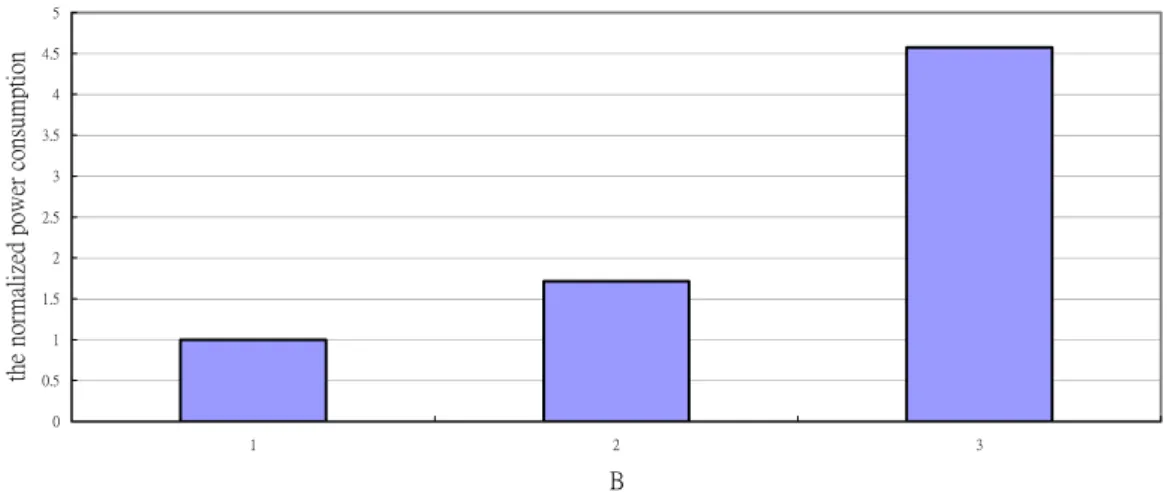
(17)From Equation (17), we can see that the total current is increasing as B increase, shown as the Figure 3.4. And if we choose a low resolution in each stage with small B, the total number of the comparators is reduced. It shows the dynamic power can be
saved. From above analysis, we can conclude that the power consumption is minimized when B=1 (2b/stage) is adopted if we only consider the settling behavior as exponential settling in a fast sample rate [15] [16] [17].
0 0.5 1 1.5 2 2.5 3 3.5 4 4.5 5 1 2 3 B the no rm al iz ed pow er c onsum pti on
Figure 3.4 the normalized total current for different stage resolution
3.2.2 The Stage Resolution with Speed Consideration
Again, the settling time constant of the MDAC is shown in Equation (14).
, ,
2
B L total L total m mC
C
g
f
g
τ
=
∼
⋅
⋅
(18)Where f = CF/(CF+CS+CP)~1/2B is the feedback factor and CL,total is the total loading
capacitance in the feedback configuration. If we have a constant gm, it shows that the large feedback and the smaller output loading capacitance can achieve the larger bandwidth. Figure 3.5 gives the particular MDAC output. And the total capacitance is
(
)
(
1)
,2
1
2
2
1
2
B opin B B L total B comp opinC
C
C
C
C
C
C
+⎡
−
+
⎤
⎣
⎦
=
+
+
+
−
C
(19)where Copin is the input capacitance of the op-amp, and Ccomp is the input capacitance
of the comparator. From Equation (19) and the feedback factor f ~1/2B, the small B allows the MDAC with large feedback factor and small load capacitance. Therefore, we can choose the small B=1 (2b/stage) for relaxing the requirement of the bandwidth
[17] [18].
Figure 3.5 the particular MDAC output
3.3 Digital Error Correction
In the practical pipelined ADC design, there is a lot of non-linearity effect which need to be reduced to the tolerable level. A number of error correction techniques have been developed to make high resolution analog-to-digital converter. The Redundant-Sign-Digit-Coding (RSD) is a digital correct algorithm which is easily implemented in digital circuits. It usually uses to overcome the comparator error. The amount of redundancy is commonly referred as 0.5 bits. This technique can relax the accuracy of the sub-ADC and keeping the gain of the stage low. For example, a 1.5 bit/stage MDAC output 2 bit digital code, but the gain of the MDAC is two, not four (22).
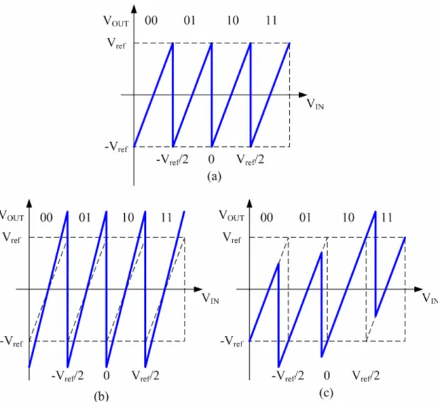
The typical output signal range of each MDAC stage is the same with the input signal range to reduce design difficulty. Figure 3.6 (a) shows the typical transfer curve of a 2 bit/stage from input to output. The comparator offset and the gain error cause over-range problems, as shown in Figure 3.6 (b) (c). This over-range error may cause the missing code at ADC output. Therefore, we need to reduce the gain of the inter
stage and add the tolerance of comparator.
Figure 3.6 (a) Ideal transfer curve of a 2/stage with (b) Gain error (c) Comparator offset
The comparator offset usually is due to the noise and the process variations. The decision level may be shifted right (a positive offset) or left (a negative offset). It may make the output code of the MDAC greater or smaller than the ideal output code. An addition and a subtraction of the output are used to avoid this error. But it is hard to determine that the comparator offset is positive or negative. Thus we can shift right the decision level by Vref/4. The digital output code is always less than or equal to its
ideal value if the comparator offset can shift the decision levels back to the left by no more than Vref/4. So we need only an addition to correct the output code. It only
shifting down the output voltage Vref/2 is used to remain within the conversion range
of the next stage from -Vref to Vref. This transfer curve is illustrated in Figure 3.7. The
dashed line is the transfer curve of 2bit stage and the solid is the modify curve. Figure 3.7 indicates that we need to correct the code in gray area by using additions. Because the modify curve with non-ideal offset has no over-range problem and require only addition correction between two original decision level. The maximum tolerable offset of the comparator is ±Vref/4.
Figure 3.7 The modify 2bit/stage transfer curve
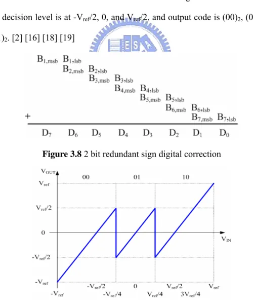
Reconstruction of the redundant sign digit code outputs is performed by adding up the properly delayed stage outputs with one-bit overlap. Figure 3.8 is an example of 2b RSD correction of 8 bit output. The LSB of stage i is added to the MSB of the stage i-1. It can be easily implemented with full adder. Thus the extra hardware caused by the error correction is very small. The 1.5 bit architecture can remove the top decision level at 3Vref/4, because the correction range is ±Vref/4, and the decision
level is Vref/4 below full scale. And the calibration technique can correct the code at
output. Figure 3.9 shows the transfer curve of 1.5 bit/stage. It is called as the 1.5 bit/stage architecture because the output code of each stage miss (11)2. The reside
transfer function of 1.5 bit/stage architecture is
=
=
=
OUT OUT OUT2
,
/ 4 , D
00
2
,
/ 4
/ 4 , D
01
2
,
/ 4 , D
10
IN ref IN refOUT IN ref IN ref
IN ref IN ref
V
V
V
V
V
V
V
V
V
V
V
V
V
⎧
+
< −
⎪
=
⎨
−
<
<
⎪
−
>
⎩
(20)where DOUT is the output code for the stage. Because the output of each stage are (00)2, (01)2, and (10)2, the 8bit ADC output code (11111111)2 is missing. Thus the last
stage should be the real 2bit flash ADC for eliminating the error. This 2bit flash ADC’s decision level is at -Vref/2, 0, and Vref/2, and output code is (00)2, (01)2, (10)2,
and (11)2. [2] [16] [18] [19]
Figure 3.8 2 bit redundant sign digital correction
An ideal behavioral model of an 8bit pipelined ADC with 1.5 bit/stage architecture is constructed by Matlab as discussed above. All parameters of the system are assumed ideal except the comparator offsets. We can observe how comparator offsets affect the output code of the system with digital error correction. First we assume the comparator in the real systems is symmetrical, so the decision level of the MDAC stage can be Vref/4+Voffset and -Vref/4-Voffset. The simulation result is illustrated
in Figure 3.10. And the INL analysis is plotted in Figure 3.11.
(a) (b)
(c)
Figure 3.10 the effect of comparator offsets for the pipelined ADC with (a) offset=0 (ideal) (b) offset=0.2 Vref (c) offset=0.3 Vref
(a)
(b)
Figure 3.11 INL of the pipelined ADC with comparator offset = (a) 0.2 Vref (b) 0.3 Vref
We can find that comparator offsets less than Vref/4 do not affect the linearity of
ADC output, but it increases INL. If the comparator offset is larger than Vref/4, the
missing codes occur ( DNL(i)=-1 ). For example, there are 28 missing codes in ADC output, shown in Figure 3.10 (c).
We can find that the Redundant-Sign-Digit-Coding provides the tolerance for comparator offset. If the ADC uses redundancy and digital correction, the effect of stage resolution on linearity is small. The comparator requirements are also relaxed, and reducing the inter stage gain allow higher speed due to the fundamental gain bandwidth tradeoff of amplifiers. The architecture of 1.5 bit/stage is shown to be effective in high throughput.
3.4 Non-ideal Considerations and Stage Requirement
Errors introduced by practical circuits are important because these errors limit the maximum performance of the ADC. In this section, an analysis of op-amp settling behavior for gain and speed is considered. And the capacitor size is considered for noise and mismatch error.
3.4.1 Residue Amplifier Gain Error
The most critical block of a pipelined stage is the multiplying D/A converter (MDAC). Figure 3.12 shows the MDAC operation from sampling phase to holding phase in 1.5 bit/stage. The finite DC gain error increases the error of analog signal. It may cause the DNL of the ADC. We can use the charge conservation principle to analysis the effect of a finite DC open-loop gain.
During sampling phase, the input signal is sampled into both capacitors CS and
CF. The total charge is Vin(CS +CF). During the holding phase, the charge on CS and
Figure 3.12 the MDAC operation
(
) (
)
(
)
IN S F DAC − S OUT − F − P
V
C
+
C
=
V
−
V C
+
V
−
V C
−
V C
(21) where the CP is the parasitic capacitance at the op-amp input, and V- is the voltage ofthe inverting input of the op-amp. Then we can get
(
S F)
S(
S F P OUT in DAC F F FC
C
C
C
C
C
V
V
V
C
C
C
−+
+
=
−
+
+
)V
(21) The feedback f during the holding phase is given byF s F P
C
f
C
C
C
=
+
+
(22)And the voltage of the inverting input of the finite gain A op-amp is
out
V
V
A
−
= −
(23)Finally, we can get an approximate Equation (24) by combining Equation (21), (22), and (23).
1
(
S F S out in DAC F FC
C
C
V
V
V
C
C
)(1
Af
)
+
≈
−
−
(24)Assuming that CS and CF are perfectly matched,
1
(2
)(1
)
out in DACV
V
V
Af
=
−
−
(25)the error is approximately 1/(Af). In order to achieve N-bit linearity, this error should
be less than 0.5/2N (0.5LSB) to prevent any missing code. Thus the requirement on
the DC gain is given by
1
2
NA
f
+>
(26)In this design, for an 8-bit ADC, the output of MDAC in the first stage constitutes the input of the following 6 stages. The maximum tolerable DNL is 0.5 LSB at 7 bit level.
We can derive that the minimum required A is 54.18dB when CP is zero. [16] [17]
3.4.2 Finite Settling Time of Op-amp
The settling time of the op-amp limits the ADC conversion speed. The analog signal must settle before next stage is holding. In section 3.2, the time constant is given by Equation (13). It assumes the settling behavior as single pole system and only time constant effect. But the system need more time to be settling by the slew-rate limited transient response. Briefly we can assume the slew-rate limited transient response took 1/3 of the settling time. Equation (13) can be re-written
t
=
(N+1) ln2
τ
⋅
(27)Where t is the time used for time constant limit can be settling. During the holding
phase, the close-loop bandwidth is f×ωu, where ωu is the unity-gain frequency of
op-amp. Therefore, the unity gain frequency of op-amp can be found:
(
1) ln
2
uN
f
t f
π
2
+
=
⋅ ⋅
(28)exponential settling is t = T/3 = 1/(3 fS). For t=6ns and Cp=Cs/4, the unity gain
frequency of the op-amp must be greater than 330MHz which feedback factor is 4/9 for 7 bit level in this design. During the slew-rate limited transient response period, the critical case is full range swing in 3ns. We can calculate the requirement of slew rate as
0.5
167 /
3
V
SlewRate
V us
ns
=
=
(29)3.4.3 Capacitor Mismatch and Size
In switched capacitor MDAC, mismatch of the sampling CS and CF capacitors is
a major error source. The matched capacitors play an important role in medium ADC design. In the previous section, the capacitors are assumed to be perfectly matched. From Equation (24), when A is infinite and let CS=C+ΔC/2, CF=C-ΔC/2, and
CS/CF~1+ΔC/2, the effect of a capacitor mismatch is given by:
(2
)
(1
)
out in DACC
C
V
V
C
C
V
Δ
Δ
≈
+
− +
(30)the approximation holds if C 1
C
Δ
<< . It given that ΔC/C of each capacitor must be less 1/2N to ensure that ΔVout is always less than an LSB.
Another consideration of capacitor is the thermal noise. A certain minimum signal capacitor size is needed to maintain adequate noise performance and dynamic range. In switch capacitor pipelined ADC, the dominating thermal noise components are the noise of the op-amp and sampling circuit. The sampling circuit is used to sample the input signal onto a sampling capacitor. The source of thermal noise is commonly referred to as kT/C noise because the noise power is proportional to kT/C where C is the size of the sample capacitor, k is Boltzmann’s constant, and T is the absolute temperature. The op-amp also contributes thermal noise degradation to the signal being processed. Although there is no general expression for the type of the
noise, in ADC based on op-amp, it is found that it is roughly equal to the switched-capacitor noise. Thus the total noise voltage introduced in an ADC stage can be approximated as
2
NkT
V
C
≈
(31)If we make the thermal noise equal to quantization noise, we can get
2 2
2
2
24
12
B full swingkT
C
kT
C
V
−⎛
⎞
Δ
=
⇒
=
⎜
⎜
⎟
⎟
⎝
⎠
(32)The minimum capacitor size for 8 bit resolution is 0.006pF for Vfull-swing is 1V. Thus
we can know that the SNR is dominated by the quantization noise for medium resolution ADC. Capacitor is found that satisfies the bandwidth requirement, and capacitor matching requirement. If the capacitor size is too large, the op-amp might not to reach the required speed. If the size is too small, the clock feed-through and charge-sharing effect will be worse. In this design, we choose the sampling capacitor size is 0.8pF for matching consideration. [20]
3.4.4 Aperture Uncertainty
In any sampling circuit, electronic noise causes random timing variations in the actual sampling clock edge. The effect of the aperture uncertainty comes about because an ADC does not sample the input at precisely equal time-intervals, as shown in Figure3.13. It adds noise to samples, especially if dVin/dt is large. The worst-case
voltage error due to the aperture jitter corresponds to sampling a sinusoidal waveform with the Nyquist frequency, which is fS/2, for example a full-scale signal
( )
full swingsin(
S)
v t
=
V
−π
f t
(33)The maximum error will occur when attempting to sample the signal v(t) at its zero-crossing, where its derivative gives the maximum slope of the signal
(0) '
S full swingv
=
π
f V
− (34)The maximum error voltage is given by the product of v’(0) and the aperture uncertainty
in S full swing
V
π
f V
−τ
Δ
≈
(35)Using Equation (35) with fs=50MHz, Vfull-swing=±1V signal, the aperture uncertainty
must less than 50ps to archive the error voltage less than a LSB. [2]
4
Circuit Design
4.1 Architecture of the ADC
In this chapter, the entire analog, clock, and digital error correction circuit are presented. The design and analysis of the circuit in each block is described. And the non-ideality of the circuit design is considered. Figure 4.1 shows the architecture of the 8 bit pipelined ADC and timing strategy. The Φ1 and Φ2 are two non-overlap clock phases which control the state of the stages. In order to cancel the charge injection error and clock feed-through, the fully differential structure and the bottom-plate technique are used in the stages. It needs two more clock phases that its falling edge is before Φ1 and Φ2. The detail is shown in the next section.
Figure 4.1 pipelined architecture used in this design and timing strategy
4.2 Sample-and-hold
Figure 4.2 Schematic diagram of Flip-Around sample-and-hold
The sample-and-hold (S/H) circuit usually plays an important role in data acquisition interface designs. S/H has dominated the performance in the pipelined ADC. The S/H is usually added in front of the ADC for better dynamic linearity at high frequency input signals. Figure 4.2 shows the schematic diagram of Flip-Around S/H. Flip-Around S/H is often used in high-speed applications. When clk2 = 1, the S/H is in the sample mode, and the input signal is sampled on the CS1 and CS2
capacitors. The edge of clk2p is rising at the same time with clk2, but the falling edge is earlier than clk2. The clk2p is used for bottom-plate technique to reduce aperture jitter and switching errors due to the sampling switches’ charge injection and clock feed-through. Thus the switches S3 and S4 are turned off before S1 and S2 for declining the charge into the sampling capacitors. The switch S7 is used for auto-zero to canceling the op-amp offset voltage. When clk1 = 1, the S/H is in hold mode, and the sampling capacitors are connected to the outputs of the op-amp. Thus the
sampling capacitors and op-amp drive the output voltage as input voltage.
Figure 4.3 the S/H operation
Figure 4.3 shows the operation of S/H in the single-end circuit. Equation (36) represents the transfer function of the S/H with the parasitical capacitor at the op-amp input:
(
)
,
1
1
(1
)
out S in S out P P out in SV
C
V
C V
V
C
V
V
A
C
V
V
A
C
− − −×
=
−
−
×
= −
⎡
⎤
≈
⎢
−
+
⎥
⎣
⎦
(36)Thus the op-amp’s input capacitor CP demands an increase in A. From above
considerations, the capacitors size of CS1 and CS2 are chosen to be 2pF to maintain the
resolution of S/H more than 8 bit. The architecture of the op-amp is a telescopic amplifier, which has an input common-mode voltage (Vicm) at 1.3V and output
common-mode voltage at 1.8V. The required DC gain (A) is 54.19dB when CP is zero,
and 60.21dB when CP = CS. And we can use the Equation (28) to find the minimum
4.2.1 Switches
Table 4.1 shows the switches type and size in Figure 4.2. The switches size must trade-off from clock feed-through and charge injection to the RC time constant. Figure 4.4 shows the RC network during sampling phase. We can assume Vin =
Vfull-swing for the worst case consideration. And the error from Vin to Vout must be less
than an LSB during the sampling period (0.5/fs). Thus we get Equation (37).
1
2
l
ON s SR
f C B
≤
n 2
(35)where the B is the required effective bit of S/H. For 8bit, 2pF sampling capacitor, and 50MHz sampling rate, the turn-on resistance must less than 900Ω. Because the switches S1, S2, S3, and S4 sample the input signal directly, those turn-on resistances must be low enough to follow the input signal. The voltage at the input of op-amp is charge to a DC voltage when S3 and S4 turn on. So using NMOS transistor is suitable. However, a charging current will flow through S3 and S4 by the varying input signal. The turn-on resistances of S3 and S4 must be low to keep the input voltage of the op-amp at the Vicm. S7 is used to make Vout+ equal to Vout- during the autozero phase.
S1 and S2 are realized by using NMOS with bootstrapped gate control voltage to reduce the distortion and device size.
Switches Switch Type W/L (um/um)
S1,S2 Bootstrapped 20/0.35(NMOS)
S5,S6 CMOS 18/0.35(NMOS), 30/0.35(PMOS)
S3,S4 NMOS 30/0.35
S7 NMOS 30/0.35
Table 4.1 switches type and size for S/H
4.2.2 Bootstrapped switch
If we can make the input error independent with the input signal, the fully-differential structure can cancel the error conceptually. Unfortunately, the turn-on resistance of the CMOS switch is dependent on the input signal. Output tracks well when the turn-on resistance is low, and tracks distorted when the input voltage is high which increases the turn-on resistance. And the actual sampling instant is variant due to the gate-to-source voltage need to be less than VTH to turn off switch.
Amplitude of third harmonic distortion will be increased due to this error. We often used the large size sampling switches or constant VGS switches to reduce this
distortion.
(a) (b)
Figure 4.5 Clock bootstrapped switch
Figure 4.5 shows the clock bootstrapped switch. It can generate a clock with constant VGS with all levels of Vin. This advantage is that the constant turn-on
resistance due to the fixed VGS make the time constant independent of the input signal.
When clk is low, the charge is VDD in Cboot. When clk is high, the Mswitch’s gate
voltage is Vin+VDD. Transistors M1, M2, M3, M4, and M8 correspond to the five
ideal switches which are shown in Figure 4.5 (a). The gate of M3 connects to the maximum voltage VG for turning off the M3, because the voltage of M3’s drain may
be higher than VDD. The M5 and M7 are added to reduce the maximum Vds of each
switches remaining within VDD. And M6 is added for turning off M4. The bulk of M3 and M4 must be connected to the highest voltage, not VDD. Figure 4.6 shows the simulation result of the bootstrapped switch with Mswitch size is 20um/0.35um. The
constant VGS is 3V due to the parasitic capacitor at the gate of Mswitch. [6] [22]
Figure 4.6 Simulation result of the clock bootstrapped switch
4.2.3 Op-amp
determine the speed and accuracy. From above considerations, the op-amp with DC gain 57dB and unity gain bandwidth 250MHz is needed for 8-bit resolution 50MS/s S/H. and the op-amp requirement of the MDAC is DC gain 56dB and unity gain bandwidth 330MHz. According to above discussion, the telescopic op-amp is adopted in our design for S/H and MDAC. The telescopic configuration is the most power efficient for similar speed performance. It typically has higher frequency capability and consumes less power than other architecture. Its high-frequency response stems from the fact that its second pole corresponding to the source nodes of the n-channel cascade devices. And its single stage architecture naturally suggests low power consumption. The disadvantage of the telescopic op-amp is limited output swing because the tail transistor cuts the output swing from both side of the output. For fully differential structure, the output swing ±1V only needs ±0.5V swing at the single output. [22]
NMOS W/L (um/um) PMOS W/L (um/um)
M1, M2 200/0.35 M5, M6 800/1
M3, M4 400/0.7 M7, M8 800/1.5
M9 600/1.5 M10 600/1.5
Table 4.2 Transistor size of telescopic op-amp
Figure 4.7 shows the architecture of the telescopic op-amp. Table 4.2 lists the size of the transistors. All transistors are biased in the saturation region. The cascode structure provides the DC open-loop gain about (gmro)2. The tail transistor (M9, M10)
is needed because it provides good PSRR and CMRR performance. The fully differential op-amp output common-mode voltage tends to drift to the supply rails due to power-supply variations, process variations, and offsets. Hence, an additional common-mode feedback loop is usually necessary. The circuit comprising the common-mode feedback loop is called the common-mode feedback circuit (CMFB).
4.2.4 CMFB
Figure 4.8 Switch capacitor CMFB circuit
The CMFB can clip the common-mode output voltage to VOCM which we
design. The main advantages of switch capacitor CMFBs are that they impose no restrictions on the maximum allowable differential input signals (op-amp outputs), have no additional parasitic poles in the common-mode loop, and are highly linear. Switch capacitor CMFBs only adopt in switch capacitor application because it will inject nonlinear clock feed-through noise into op-amp. The switch capacitor CMFBs also increase the output capacitance that needs to be driven by op-amp. The switch capacitor CMFB is adopted in this design because it allows a larger output swing. In actual design, we must keep the gain of the CMFB loop large enough to keep the common-mode voltage of op-amp output as the VOCM. But the large feedback factor
often cause unstable. Thus we choose C1 and C2 are 400f, C3 and C4 are 200f. And M9 is used to decrease the unity-gain frequency of the gain in the CMFB loop to keep circuit stable. S2 and S4 use NMOS switch, and other switches use CMOS switch. Those must be small to minimize the errors due to the leakage current and charge injection. When all voltage is steady, we can get Equation (36):
V
, mod
out common e ctrl OCM bias
V
−−
V
=
V
−
(36)If the gain of CMFB loop is large, the Vctrl is close to Vbias. Thus we can get the output
common-mode voltage that is almost the same as VOCM. [23] [24]
4.2.5 Op-amp Bias Circuit
Figure 4.9 shows the telescopic op-amp with bias circuit and Table 4.3 shows the size of each transistor. Mb1-Mb6 are used as cascode current mirror. Mb7-Mb9 are used to generate the bias voltage Vb1 and Vb2. Mb8 and Mb9 comprise wide-swing current mirror [13]. The basic ideal of the current mirror is to bias the drain-source voltages of Mb8 and Mb9 to be close to the minimum possible without Mb8 and Mb9 going into the triode region. Because of the minimum drain-source voltage the output swing of the op-amp can be more. Mb15 is used to provide a bias voltage which is
![Figure 1.1 A/D interface between the external world and digital system [2] As the CMOS processing improved, the MOS device has kept shrinking minimum feature size and greatly impacted the performance of digital circuits](https://thumb-ap.123doks.com/thumbv2/9libinfo/8063612.163084/14.892.155.740.108.326/interface-external-processing-improved-shrinking-impacted-performance-circuits.webp)