行政院國家科學委員會專題研究計畫 成果報告
多晶薄膜電晶體通道層缺陷分布分析與多晶鍺薄膜電晶體
之研製
計畫類別: 個別型計畫 計畫編號: NSC93-2215-E-009-079- 執行期間: 93 年 08 月 01 日至 94 年 07 月 31 日 執行單位: 國立交通大學電子工程學系暨電子研究所 計畫主持人: 林鴻志 計畫參與人員: 葉冠麟、李明賢、蘇俊榮、房新原、蘇育正 報告類型: 精簡報告 處理方式: 本計畫可公開查詢中 華 民 國 94 年 11 月 7 日
行政院國家科學委員會補助專題研究計畫
■ 成 果 報 告
□期中進度報告
多晶薄膜電晶體通道層缺陷分布分析與多晶鍺薄膜電
晶體之研製
計畫類別:■個別型計畫 □ 整合型計畫
計畫編號:NSC 93-2215-E-009 -079-
執行期間:2004 年 8 月 1 日至 2005 年 7 月 31 日
計畫主持人:
林鴻志
共同主持人:
計畫參與人員:
葉冠麟、李明賢、
蘇俊榮、房新原、蘇育正
成果報告類型(依經費核定清單規定繳交):■精簡報告 □完整報告
本成果報告包括以下應繳交之附件:
□赴國外出差或研習心得報告一份
□赴大陸地區出差或研習心得報告一份
□出席國際學術會議心得報告及發表之論文各一份
□國際合作研究計畫國外研究報告書一份
處理方式:除產學合作研究計畫、提升產業技術及人才培育研究計畫、
列管計畫及下列情形者外,得立即公開查詢
□涉及專利或其他智慧財產權,□一年□二年後可公開查詢
執行單位:
國立交通大學 電子研究所
中文摘要: 在本報告中,我們提出並成功演示一種先進方式,能在萃取薄膜電晶體元件通道 區的全能障區缺陷密度。在這種方式中,我們將場效電導法應用在一具有場引發源/汲 極之蕭特基複晶矽膜薄電晶體。僅需要單一個電晶體和兩條在室溫之下的次臨界電流-電壓量測即可萃取出全能障區缺陷密度。不同製程處理的影響可以用這個方法清楚地 鑑別出來。 我們也觀察了電性量測和結構參數對於萃取結果的影響,用以得到最佳的測試條 件。我們的研究顯示通道中的寄生電阻會造成尾態密度的過度高估。精準的缺陷密度 可以藉由足夠高的汲極電壓,足夠高的副閘極電壓,和夠短的場引發源/汲極長度。 關鍵字: 複晶矽,缺陷密度,場引發汲極,蕭特基複晶矽薄膜電晶體,全能障區缺陷密度 英文摘要:
In this work, we have proposed and successfully demonstrated a novel approach to obtain the full band-gap DOS in the channel of TFT devices. In this approach, the field-effect conductance method is performed on an Schottky barrier (SB) poly-Si TFT with electrical source/drain extensions induced by a field-plate. Only one single device and two simple subthreshold I-V measurements at room temperature are needed for full band-gap DOS extraction. Impacts of different process treatments are clearly resolved using this methodology.
We have also characterized the dependence of both electrical and structural parameters on the measurement results in order to set suitable test conditions. Our results indicate that the parasitic resistance presenting in the channel would result in an overestimation of tail state density. Accurate DOS extraction can be obtained by employing sufficiently high drain and sub-gate biases and short electrical source/drain extensions.
Keywords:
Introduction
Poly-Si TFTs have been investigated extensively due to their applications in large-area electronics like flat-panel displays. The operation of poly-Si TFTs is more complicated compared with their single-crystal counterpart due to the existence of grain boundaries in the channel, since the defects at and inside the grain boundaries may increase the off-state leakage, retard the device turn-on, and impede the carrier transport [1]. Accurate modeling of poly-Si TFT behavior is thus indispensable for simulation and design of poly-Si TFT circuits. This requires precise determination of the effective density-of-states (DOS) distribution within the poly-Si band gap. Previously, field-effect conductance (FEC) method [2-4] which characterizes the subthreshold conductance of devices has been employed to
extract DOS. Fig. 1 shows the flow chart of FEC analysis. Detailed theoretical background
of FEC could be found in [2] and [3]. Briefly, three major steps are involved: (a) determination of flat-band voltage, VFB, (b) determination of relationship between VG and surface potential, ? s, and (c) calculation of DOS as a function of E-EF within the gap. In step (a), VFB can be determined as the VG when the term T•[d(logG)/dVG] is independent of temperature. (T is temperature, G is ID/VD) [5]. In step (b), either the “incremental method” or the “temperature method” can be adopted[4] . To obtain full band-gap DOS, at least one n-channel device and one p-channel device are needed for characterization. Besides, I-V measurements need to be performed at various temperatures, making the procedure very tedious and time-consuming. In this work, we present a novel methodology to address this issue. In this scheme, all we need for full band-gap DOS extraction are only one device and two I-V measurements performed at room temperature. The whole process is thus greatly simplified and shortened.
Structure of the Test Device
The characterization is performed on a Schottky barrier (SB) TFT which features metallic (CoSi) source/drain and a sub-gate lying over the passivation oxide [6, 7], as shown in Fig. 2. During operation, electrical source/drain extensions are induced in the channel offset regions underneath the gate sidewall spacers by applying a high voltage on the
sub-gate (or the field-plate). Depending on the polarity of sub-gate bias, the device could be set for either n-or p-channel operation. The formation of electrical junctions could also dramatically reduce the off-state leakage [7], which is essential for the analysis. To reduce the impact of series resistance on the analysis, self-aligned sidewall spacers were used to define the channel offset regions. By exploiting the ambipolar characteristics of
Schottky-barrier (SB) TFTs, full band-gap DOS can be obtained on a single device. Detailed device fabrication and operation could be found in our previous reports [6, 7].
Experimental Results
A. Determination of VFB by temperature method
determine VFB. In this work we found that the FB extracted from n-channel operation coincides well with that of p-channel operation with the same device. An example is shown in Fig.3 in which T[d(logG)/dVG] is expressed as a function of 1000/T. In the figures, the results for both p- and n-channel operations indicate that VFB is
around –2.1 V at which T[d(logG)/dVG] is almost independent of temperature. This consistency between the two operation modes is expected and confirms the validity of this method.
B. DOS extraction
Next, we used both the “incremental method” and the “temperature method” to extract DOS. Ambipolar subthreshold I-V characteristics measured at various temperatures are show in Fig. 4. For the “temperature method”, Arrehenius plots of
dG/dVG and the corresponding EA as a function of VG are shown in Fig. 5 and Fig. 6,
respectively. Good agreement in the extracted DOS between the two methods is
obtained, as shown in Fig. 7. We have also performed the incremental method” at room temperature and 55 °C to check if ambient temperature will cause any disparity on the results. As can be seen in Fig. 8, no significant difference is observed between the two characterizations.
C. Effects of process treatments
It’s well known that the DOS of poly-Si TFT is closely related to the channel preparation methods and the process conditions. In this work the new DOS
characterization scheme was also employed to study the impact of different process treatments on the device characteristics. Fig. 9 illustrates the effect of plasma
hydrogenation performed in an NH3 plasma at 300 °C for one hour. As can be seen in
the figure that such plasma treatment is useful in reducing the DOS, especially for those located near the mid-gap level.
Fig.10 compares the DOS characteristics of devices with channel prepared by three different schemes, namely, as-deposited poly-Si, solid-phase crystallization (SPC), and excimer laser annealing (ELA). Among those splits the ELA sample shows lowest DOS value. Figs. 11 (a) and (b) show the TEM pictures for SPC and ELA samples, respectively. The larger grain size observed in the ELA sample explains the results shown in Fig.10. The above results indicate that the proposed methodology is useful in resolving the effects of different process treatments on the material and device
characteristics.
D. A new way for determining VFB
Finally, an important finding is discovered during the course of this study. Specifically, we observed that the extracted FB using the tedious conventional temperature scheme coincides well with the VG value at the intersection point of the bi-channel I-V curves measured at room temperature. An example can be found by comparing Fig. 3 and Fig. 4. To further validate the universality of this observation, different groups of samples were characterized and the results are summarized in Fig. 12. It can be seen that good agreements are obtained in all cases. This important finding
thus provides a new and much simpler methodology for the determination of VFB.
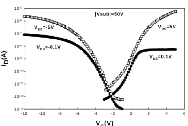
E. Effect of Applied Drain Bias
Here we address the effect of drain bias on the measurement results. The measurements were carried out for n-channel operation by sweeping gate voltages from –3 to +6V, and for p-channel operation by sweeping gate voltages from –1 to –10 V, with drain voltages |VDS|= 0.1V or 5V, and sub-gate voltage |Vsub|=50V. Fig. 13
shows the characteristics of the ID-VG for the FID SB-TFT with CoSi2 S/D material.
The channel film is SPC poly-Si film. As can be seen in the figure, the on-current in n-channel operation is more sensitive to VDS than p-channel operation, owing to the
higher barrier height of electrons than holes at the CoSi2/Si contact. The extracted DOS
results are shown in Fig. 14. It is observed that the DOS remains unaffected in the mid-gap regime, but increases significantly near the band edge when |VDS| is set at 0.1V,
especially for the conduction band edge. It was shown previously that the increase in |VDS| could decrease the source-side carrier tunneling distance [6-8], and thus the
parasitic resistance. As the Fermi level moves toward the band edge, the operation is near threshold and becomes more sensitive to the contact resistance. As a result, the DOS is overestimated when |VDS| is not sufficiently high.
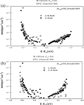
F. Effects of the channel length
Fig. 15~18 shows the extracted DOS for four devices with self-aligned spacer and channel length ranging from 0.8 to 5 µm. The on-current measured at |VDS| = 0.1 V as a
function of channel length for these devices is shown in Fig.19. The on current
becomes larger as the channel length becomes shorter due to reduced channel resistance. However, the n-mode current is almost independent of channel length when channel length is lager than 1 µm, indicating the significance of contact resistance due to larger electron barrier height. In these measurements, the mid-gap DOS is almost the same (about 1.2x10¹⁸ eV-1cm-3), while the tail DOS is strongly dependent of the applied bias conditions. Fig. 20 (a) & (b) compare the DOS results among devices with different channel length and |VDS| of 5 V. It can be seen that reasonable agreement is achieved
among these devices, indicating that |VDS| of 5 V is sufficient large so the effects of
parasitic resistance is insignificant.
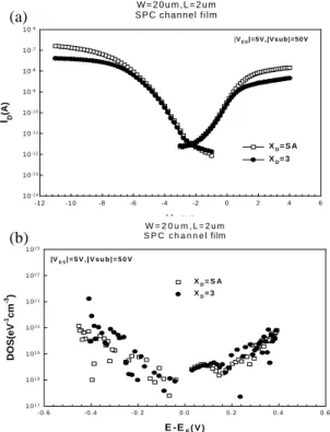
G. Effects of drain-side extension length
Fig. 21 (a) shows the ambipolar transfer characteristics of device with self-aligned and non-self-aligned (XD = 3 µm) FID length under |VDS| of 0.1V. The extracted DOS
results are shown in Fig. 21 (b). It can be seen that the on-state current is significantly lower for device with XD of 3µm. This is apparently due to the larger parasitic
resistance in the FID region and thus leads to an overestimation of tail DOS, as shown in Fig. 21 (b). Such disparity can, again, be removed by increasing the |VDS| to 5 V, as
Discussion and Conclusion
Using the new methodology, the overall DOS extraction procedure for TFT can be greatly simplified compared to the conventional scheme (TABLE I). In short, only a single device and two simple subthreshold I-V measurements at room temperature are all that needed for full band-gap DOS extraction. In addition, the new methodology lends itself handily to automatic measurement system. It is very simple and useful for TFT technology development as well as practical manufacturing, since the device structure (Fig. 2) and layout are compatible with modern TFT technology. In particular, the sub-gate can be
formed simultaneously with the metal pad, so no extra mask is needed. And the formation of the metallic source/drain could be cleverly incorporated into the baseline by skipping the source/drain implant in the DOS test structure.
We have also characterized the dependence of both electrical and structural parameters on the measurement results in order to set suitable test conditions. Our results indicate that the parasitic resistance presenting in the channel would result in overestimation of tail state density. A sufficiently high drain and sub-gate biases and short electrical junction length are thus needed.
In this work, only the defect states contained in the channel are considered, though more precise DOS extraction is possible if the oxide interface states are also taken into account [9]. This will be the main subject of our future work.
Fig. 1 Flow chart for extracting DOS in TFT using conventional FEC method.
Fig. 2 Structure of poly-Si SB-TFT featuring silicide source/drain and a sub-gate lying over the passivation oxide.
Fig. 3 T[d(logG)/dVG] vs. 1000/T for (a) a- and (b) p-channel operations of a SB poly-Si TFT. In both cases, VFB is determined to be around –2.1V.
Fig.4 Ambipolar subthreshold I-V characteristics of a SB poly-Si TFT measured at various
Fig. 5 Arrhenius plots of ln (dG/dVG) extracted from Fig. 4
Fig. 6 Activation energy extracted from Figs. 4 and. 5.
Fig. 7 DOS results obtained by using incremental method and temperature method.
Fig. 8 DOS results obtained by using incremental method performed on ambipolar subthreshold I-V characteristics measured at 25 and 55 °C
Fig. 9 Effects of plasma treatment on the DOS of devices. temperature method. The results indicate that 1-hour NH3 treatment is effective in reducing the mid-gap defect density.
Fig. 10 Effects of different recrystallization treatments on the DOS of devices.
Fig. 11 TEM pictures of characterized samples that received (a) solid-phase crystallization (SPC), and (b) excimer laser annealing (ELA) treatments. The larger grain size in ELA sample well
explains its low extracted DOS shown in Fig. 10.
Fig. 12 Comparison of VFB values determined using the
conventional temperature method and the new methodology performed on two groups of devices with various parameters.
W=20um,L=2um,XD=XS=1um,SPC channel film
VG(V) -12 -10 -8 -6 -4 -2 0 2 4 6 I D (A) 10-13 10-12 10-11 10-10 10-9 10-8 10-7 10-6 10-5 VDS=0.1V VDS=5V VDS=-5V VDS=-0.1V |Vsub|=50V
Fig. 13 Ambipolar transfer characteristics in both low and high drain bias
W=20um,L=2um,XD=XS=1um,SPC channel film
E-EF(eV) -0.6 -0.4 -0.2 0.0 0.2 0.4 0.6 DOS(eV -1 cm -3 ) 1018 1019 1020 1021 1022 1023 1024 VDS=0.1V VDS=-0.1V VDS=5V VDS=-5V
Fig. 14 Full-band gap DOS extracted at |VDS| of 0.1 and
5 V W = 8 0 u m , L = 0 . 8 u m , XD= S A , S P C c h a n n e l film E - E F ( e V ) 0 DOS(eV -1cm -3) 1 01 8 1 01 9 1 02 0 1 02 1 1 02 2 1 02 3 1 02 4 |VD S| = 0 . 1 V |VD S| = 5 V 0 . 6 0 . 4 0 . 2 -0.2 - 0 . 4 - 0 . 6
Fig. 15 The extracted DOS results in a device with channel length of 0.8um.
W=80um,L=1um,XD=SA SPC channel film E-EF(eV) -0.6 -0.4 -0.2 0.0 0.2 0.4 0.6 DOS(eV -1 cm -3 ) 1018 1019 1020 1021 1022 1023 1024 |VDS|=0.1V |VDS|=0.1V |Vsub|=50V
Fig. 16 The extracted DOS results in a device with channel length of 1um.
W = 8 0 u m , L = 2 u m , X = S A SPC channel film E-EF(eV) -0.6 -0.4 -0.2 0.0 0.2 0.4 0.6 DOS(eV -1cm -3) 1 018 1 019 1 020 1 021 1 022 1 023 1 024 |VD S|=0.1V |VD S|=5V
Fig. 17 The extracted DOS results in a device with channel length of 2um.
W = 8 0 u m , L = 5 u m , X = S A S P C c h a n n e l f i l m E -EF( e V ) 0 DOS(eV -1cm -3) 1 01 8 1 01 9 1 02 0 1 02 1 1 02 2 1 02 3 1 02 4 0.6 -0.6 -0.4 -0.2 0.2 0.4 |VD S| = 0 . 1 V |VD S| = 5 V
Fig. 18 The extracted DOS results in a device with channel length of 5um.
O n c u r r e n t v e r s u s c h a n n e l l e n g t h On current(A) 1 0- 1 1 1 0- 1 0 1 0-9 1 0-8 1 0-7 1 0-6 N - c h a n n e l o p e r a t i o n P - c h a n n e l o p e r a t i o n W = 8 0 u m , | VD S| = 0 . 1 V , | V s u b | = 5 0 V S P C c h a n n e l f i l m
Fig. 19 On current vs. channel length
W = 8 0 u m , XD= S A S P C c h a n n e l film E - EF( e V ) - 0 . 6 - 0 . 4 - 0 . 2 0 . 0 0 . 2 0 . 4 0 . 6 DOS(eV -1cm -3) 1 01 8 1 01 9 1 02 0 1 02 1 1 02 2 1 02 3 1 02 4 L = 5 u m L = 0 . 8 u m 0 . 6 - 0 . 6 - 0 . 4 0 . 4 |VD S| = 5 V , | V s u b | = 5 0 V 0 . 2 - 0 . 2 W = 8 0 u m ,XD= S A , S P C c h a n n e l film E -EF( e V ) - 0 . 6 - 0 . 4 - 0 . 2 0 . 0 0 . 2 0 . 4 0 . 6 DOS(eV -1cm -3) 1 01 8 1 01 9 1 02 0 1 02 1 1 02 2 1 02 3 1 02 4 L = 0 . 8 u m L = 2 u m | VD S| = 5 V , | V s u b | = 5 0 V (a) (b)
Fig. 20(a), (b) Comparison of DOS extracted in devices with various channel length.
W = 2 0 u m , L = 2 u m SPC channel film E -EF( V ) -0.6 -0.4 -0.2 0.0 0.2 0.4 0.6 DOS(eV -1cm -3) 1 017 1 018 1 019 1 020 1 021 1 022 1 023 XD= 3 XD= S A |V D S |=0.1V ,|Vsub|=50V 0.6 0.4 0.2 -0.2 -0.4 -0.6 (a) W = 2 0 u m , L = 2 u m S P C c h a n n e l film VG( V ) -12 - 1 0 -8 -6 -4 -2 0 2 4 6 ID (A) 1 0- 1 3 1 0- 1 2 1 0- 1 1 1 0- 1 0 1 0-9 1 0-8 1 0-7 1 0-6 1 0-5 |V D S |=0.1V ,|Vsub|=50V XD= 3 u m XD= 3 u m XD= S A XD= S A (b)
Fig. 21 (a)Ambipolar transfer characteristics of deices with various drain-side offset length at |VDS| of
0.1 V. (b)Full-band gap DOS extracted deices with various drain-side offset length at |VDS| of
W = 2 0 u m , L = 2 u m SPC channel film VG( V ) - 1 2 -10 -8 -6 -4 -2 0 2 4 6 ID (A) 1 0-14 1 0-13 1 0-12 1 0-11 1 0-10 1 0-9 1 0-8 1 0-7 1 0-6 XD= S A XD= 3 |VD S| = 5 V , | V s u b | = 5 0 V W = 2 0 u m , L = 2 u m S P C c h a n n e l film E -EF( V ) -0.6 - 0 . 4 - 0 . 2 0 . 0 0 . 2 0 . 4 0 . 6 DOS(eV -1cm -3) 1 01 7 1 01 8 1 01 9 1 02 0 1 02 1 1 02 2 1 02 3 XD= S A XD= 3 |VD S| = 5 V , | V s u b | = 5 0 V (a) (b)
Fig. 22 (a) Ambipolar transfer characteristics of deices with variousdrain-side offset length at |VDS| of 5
V. (b) Full-band gap DOS extracted deices with various drain-side offset length at |VDS| of 5 V
References:
[1] I.-W. Wu, T.-Y. Huang, W.B. Jackson, A.G. Lewis and A. Chiang, "Passivation kinetics of two types of defects in polysilicon TFT by plasma hydrogenation," Electron Device Letters, IEEE, vol. 12, pp. 181-183, 1991.
[2] G. Fortunato and P. Migliorato, "Determination of gap state density in polycrystalline silicon by field-effect conductance," Appl. Phys. Lett., vol. 49, pp. 1025-1027, October 20, 1986. 1986.
[3] G. Fortunato, D.B. Meakin, P. Migliorato and P.G. Le Comber, "Field-effect analysis for the determination of gap-state density and Fermi temperature in polycrystalline silicon," Philos.
Mag., vol. B57, pp. 573-586, May. 1988.
[4] T. King, M.G. Hack and I. -W. Wu, "Effective density-of-states distributions for accurate modeling of polycrystalline-silicon thin-film transistors," J. Appl. Phys., vol. 75, pp. 908-913, January 15, 1994. 1994.
[5] R.L. Wiesfield and D.A. Anderson, "An improved field-effect analysis for the determination of the pseudogap-state density in amorphous semiconductor," Philos. Mag., vol. B44, pp. 83-93, January 1981. 1981.
[6] H.C. Lin, C.Y. Lin, K.L. Yeh, R.G. Huang, M.F. Wang, C.M. Yu, T.Y. Huang and S.M. Sze, "A novel implantless MOS thin-film transistor with simple processing, excellent performance and ambipolar operation capability," pp. 857-859.
[7] H.-C. Lin, K.-L. Yeh, T.-Y. Huang, R.-G. Huang and S.M. Sze, "Ambipolar Schottky-barrier TFTs," Electron Devices, IEEE Transactions on, vol. 49, pp. 264-270, 2002.
[8] H.C. Lin, K.L. Yeh, R.G. Huang, C.Y. Lin and T.Y. Huang, "Schottky barrier thin-film transistor (SBTFT) with silicided source/drain and field-induced drain extension," Electron
Device Letters, IEEE, vol. 22, pp. 179-181, 2001.
[9] O.K.B. Lui, S.W.-B. Tam, P. Migliorato and T. Shimoda, "Method for the determination of bulk and interface density of states in thin-film transistors," J. Appl. Phys., vol. 89, pp. 6453-6458, June 1, 2001. 2001.
本計劃已發表成果:
IEDM’2004, pp. 781- 784
Electrochemical and Solid-State Letters, Vol.8, pp. G249- G250 (2005) 另外數篇國際論文送審中