國 立 交 通 大 學
電子工程學系 電子研究所碩士班
碩 士 論 文
利用大氣電漿沉積以氧化鋅為主的透明導電膜
其光電特性和熱穩定性的研究
Investigation on Opto-electrical Properties and Thermal
Stability of Zinc Oxide Based Transparent Conductive Oxides
Prepared by Atmospheric Pressure Plasma Jet
研 究 生 : 林煒力
指導教授 : 張 國 明 博士
中華民國
中華民國
中華民國
利用大氣電漿沉積以氧化鋅為主的透明導電膜
其光電特性和熱穩定性的研究
Investigation on Opto-electrical Properties and Thermal
Stability of Zinc Oxide Based Transparent Conductive Oxides
Prepared by Atmospheric Pressure Plasma Jet
研 究 生:林煒力 Student:Wei-Li Lin
指導教授:張國明 博士 Advisor:Dr. Kow-Ming Chang
國 立 交 通 大 學
電子工程學系 電子研究所碩士班
碩 士 論 文
A Thesis
Submitted to Department of Electronics Engineering and Institute of Electronics College of Electrical and Computer Engineering
National Chiao Tung University in Partial Fulfillment of the Requirements
for the Degree of Master in Electronics Engineering August 2010 Hsinchu, Taiwan
中華民國九十
中華民國九十
中華民國九十
中華民國九十九
九
九年八月
九
年八月
年八月
年八月
利用大氣電漿沉積以氧化鋅為主的透明導電膜
其光電特性和熱穩定性的研究
研究生:林煒力 指導教授:張國明 博士國 立 交 通 大 學
電子工程學系 電子研究所碩士班
摘要
摘要
摘要
摘要
於本論文中,我們利用大氣電漿化學氣相沉積法去成長以氧化鋅 為主的透明導電膜,包含了氧化鋅摻雜銦、氧化鋅摻雜鋁和氧化鋅摻 雜鎵。我們將研究不同的摻雜濃度和基板溫度對這些薄膜在表面型 態、結構、電性和光學的影響。並且我們也將探討氧化鋅摻雜銦和氧 化鋅摻雜鎵在高溫處理下的熱穩定性。所有薄膜都顯現出垂直基板之 (002)晶向的結構。掺雜八個原子百分濃度和兩百度的氧化鋅摻雜銦 有最佳的電性表現,電阻值為 1.71E-3 Ωcm。氧化鋅摻雜銦在光學性 質上的表現都比氧化鋅摻雜鋁好,穿透率在可見光範圍約 85%左右。 在熱穩定性的表現上面,即使在高溫的氧氣環境下,氧化鋅摻雜銦的 穩定性仍比氧化鋅摻雜鎵還要好。我們的研究顯示:氧化鋅摻雜銦是 很有希望被應用在下一個世代的透明導電薄膜上面。
Investigation on Opto-electrical Properties and Thermal
Stability of Zinc Oxide Based Transparent Conductive Oxides
Prepared by Atmospheric Pressure Plasma Jet
Student:Wei-Li Lin Advisor:Dr. Kow-Ming Chang
Department of Electronics Engineering and Institute of Electronics National Chiao Tung University, Hsinchu, Taiwan
Abstract
In this thesis, we use the APPCVD system to deposit the ZnO based transparent conductive oxides (TCO), including IZO, AZO and GZO. The effect of different doping concentration and substrate temperature on the morphological, structural, electrical and optical properties of the thin films has been investigated. Moreover, we investigate the thermal stability of IZO and GZO at different annealing conditions. All films show the preferred (002) orientation perpendicular to the substrate. The minimum resistivity of 1.7E-3 Ωcm was obtained at a substrate temperature of 200℃ and 8 at% indium-doped. The transmittance of IZO thin films were around 85% in the visible spectrum. The IZO thin films show better transmittance than the AZO films. It is shown that the IZO thin films show better thermal stability than GZO films even in oxygen ambient at high temperature. Our study shows that the IZO thin films were a promising candidate for next generation TCO applications.
誌
誌
誌
誌 謝
謝
謝
謝
於本人碩士求學時間中,我首先要感謝指導老師張國明教授,讓 我在研究和平常的做人處世上都獲益良多。除此之外,感謝王水進教 授和龔正教授在口試中,對我的論文研究有進一步的探討和指教,讓 我的想法可以更加廣泛。 其次感謝實驗室學長們的熱心指導,尤其是黃菘宏學長,在我的 研究上提供了許多寶貴的意見,讓我可以順利的進行自己的實驗研 究。另外也要感謝工業技術研究院(ITRI)、國家奈米元件實驗室(NDL) 與國立交通大學奈米中心(NFC)提供良好的研究機台和實驗環境,讓 我們能心無旁鶩的做好自己的實驗;且也要感謝林哲蔚先生、何惟梅 小姐、姚潔宜小姐和沈奕伶小姐等人的協助下,讓我可以順利的進行 並完成實驗的研究。 接著,我要感謝實驗室的同學們在我研究有問題的時候可以一起 討論,並且提供適切的意見來幫助我,尤其是實驗夥伴吉家威和陳偉 強在實驗上的助益更為重要,還有同組的學弟蔣偉韓能盡他所能幫助 之力幫助我,才得以完成此論文。 最後,我要特別感謝家人對我的幫助和支持,女友思勻的陪伴, 讓我可以順利的完成碩士學位。Contents
Abstract (Chinese) ···i
Abstract (English) ··· ii
Acknowledgement··· iii
Chapter 1 Introduction ···1
1.1Transparent Conductive Oxide (TCO)···1
1.2TCO deposition method···3
1.3Motivation···4
Chapter 2 Literature Review···7
2.1 Properties of ZnO···7
2.2 Deposition methods of TCO films···9
2.3 Atmospheric-pressure plasma system···23
Chapter 3 Experiments ···35
3.1 Experimental procedures···35
3.2 Experimental equipments and parameters···39
3.3 Characterization analysis equipments···43
Chapter 4 Result and Discussion···52
4.1 Electrical and optical characterization···53
4.2 Thermal stability···66
Chapter 5 Conclusion ···127
Chapter 6 Future Work ···128
Table Captions
Table 1-1 The basic properties of three in common used TCO films ···5
Table 1-2 Application of TCO films···6
Table 2-1 Comparison of ALD and CVD ...27
Table 2-2 Thin film deposition methods compared ...27
Table 2-3 Density of charge species in the plasma discharge ...34
Table 3-1 Composition and characteristics of FL glasses ···38
Table 3-2 Characteristics of AN100 glasses ···39
Table 3-3 Parameters of TCO thin films···41
Table 3-4 Parameters of thermal stability experiments ···42
Table 3-5 Characterization analysis equipments···51
Table 4-1 Whole data with different In concentration of IZO films··· 116
Table 4-2 Whole data with different Al concentration of AZO films···· 117
Table 4-3 Whole data with different substrate temperature of IZO films ··· 118
Table 4-4 Whole data with different substrate temperature of AZO films ··· 119
Table 4-5 Whole data with different annealing temperature in nitrogen ambient of GZO films ··· 120
Table 4-6 Whole data with different annealing temperature in nitrogen ambient of IZO films··· 121
Table 4-7 Whole data with different annealing temperature in nitrogen ambient of ZnO films ··· 122
Table 4-8 Whole data with different annealing temperature in oxygen ambient of GZO films ··· 123 Table 4-9 Whole data with different annealing temperature in oxygen
ambient of IZO films··· 124 Table 4-10 Whole data with different annealing temperature in oxygen
Figure Captions
Figure 2-1 ZnO crystal structures···28
Figure 2-2 Schematic illustration of magnetron sputtering ···28
Figure 2-3 Schematic illustration of ARE which is used the hot electron emitter ···29
Figure 2-4 Schematic illustration of ARE which is used the RF discharge ···29
Figure 2-5 Schematic illustration of a Pulsed laser deposition system····30
Figure 2-6 Description of the deposition process with raising the substrate temperature ···30
Figure 2-7 Schematic illustration of equipment for spray pyrolysis deposition···30
Figure 2-8 Steps of the dip coating process···31
Figure 2-9 Schematic illustration of principle for ALD···31
Figure 2-10 Sequence of events during CVD ···32
Figure 2-11 Development of boundary layer in a horizontal reactor···32
Figure 2-12 Surface reaction and mass transit limited growth in CVD···32
Figure 2-13 Schematic the principle of corona discharge ···33
Figure 2-14 Schematic illustration of the DBD configurations···33
Figure 2-15 Schematic illustration of the AP plasma jet structures ···33
Figure 2-16 Schematic illustration of the arc plasma···34
Figure 3-1 Schematic illustration of TCO thin films investigation ···35
Figure 3-2 Schematic illustration of thermal stability investigation of TCO thin films ···36
Figure 3-4 Schematic illustration of TCO thin films prepared with
APPCVD···40
Figure 3-5 APPCVD system of ITRI ···40
Figure 3-6 Schematic illustration of SEM instrument ···50
Figure 3-7 Schematic illustration of four point probe principle ···50
Figure 3-8 Schematic illustration of Hall Effect principle ···51
Figure 3-9 Schematic illustration of haze measurement principle ···51
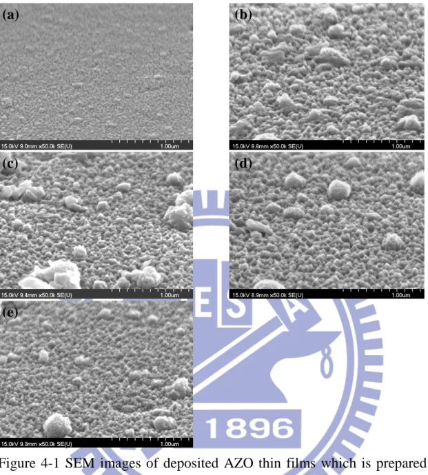
Figure 4-1 SEM images of deposited AZO thin films which is prepared with different Al concentration···71
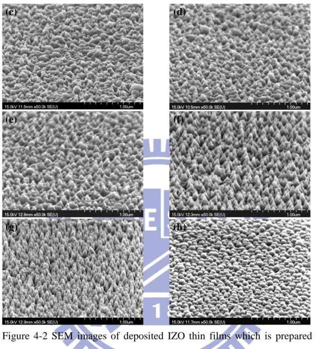
Figure 4-2 SEM images of deposited IZO thin films which is prepared with different In concentration ···72
Figure 4-3 SEM images of deposited AZO thin films which is prepared with different substrate temperature ···73
Figure 4-4 SEM images of deposited IZO thin films which is prepared with different substrate temperature ···73
Figure 4-5 AFM images of deposited IZO thin films which is prepared with different In concentration ···74
Figure 4-6 AFM images of deposited IZO thin films which is prepared with different substrate temperature ···75
Figure 4-7 GIXRD patterns of ZnO and AZO thin films deposited with different Al concentration···75
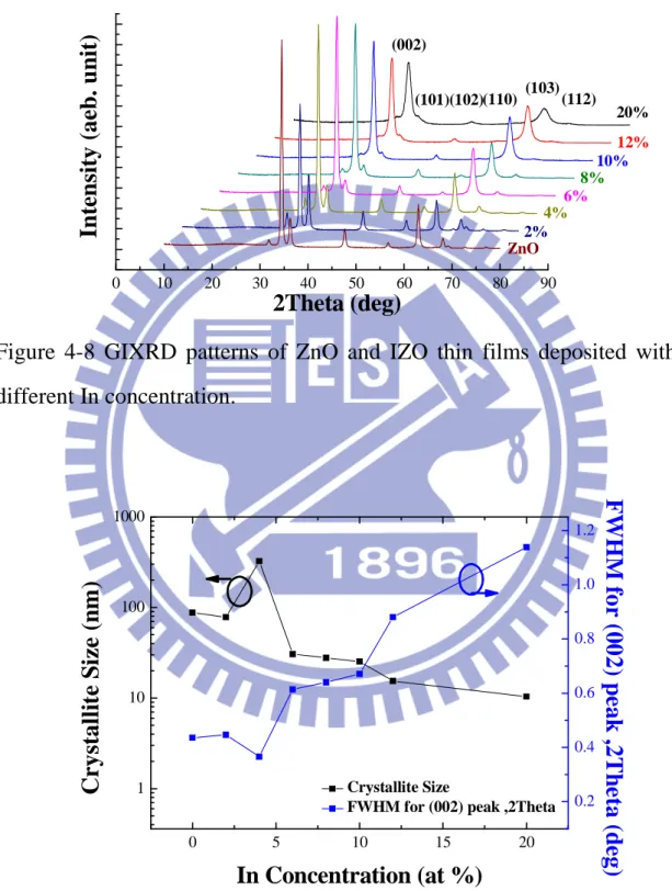
Figure 4-8 GIXRD patterns of ZnO and IZO thin films deposited with different In concentration ···76
Figure 4-9 Variation of crystallite size and the FWHM for (002) peak of IZO thin films with different In concentration ···76
Figure 4-10 Variation of crystallite size and the FWHM for (002) peak of GZO thin films with different Ga concentration ···77 Figure 4-11 Variation of crystallite size and the FWHM for (002) peak of
AZO thin films with different Al concentration ···77 Figure 4-12 Variation of crystallite size and the FWHM for (002) peak of
IZO thin films with different substrate temperature ···78 Figure 4-13 Variation of crystallite size and the FWHM for (002) peak of
AZO thin films with different substrate temperature···78 Figure 4-14 Decreasing of the (002) peak position of IZO thin films with
different In concentration ···79 Figure 4-15 Increasing of the (002) peak position of AZO thin films with
different Al concentration···79 Figure 4-16 Increasing of the (002) peak position of GZO thin films with
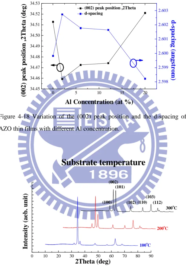
different Ga concentration ···80 Figure 4-17 Variation of the (002) peak position and the d-spacing of IZO thin films with different In concentration ···80 Figure 4-18 Variation of the (002) peak position and the d-spacing of
AZO thin films with different Al concentration ···81 Figure 4-19 GIXRD patterns of AZO thin films deposited with different
substrate temperature···81 Figure 4-20 GIXRD patterns of IZO thin films deposited with different
substrate temperature···82 Figure 4-21 Variation of the resistivity, carrier concentration and hall
mobility of IZO thin films with different In concentration··82 Figure 4-22 Variation of the resistivity, carrier concentration and hall
temperature···83 Figure 4-23 Variation of the resistivity, carrier concentration and hall
mobility of AZO thin films with different Al concentration83 Figure 4-24 Variation of the resistivity, carrier concentration and hall
mobility of AZO thin films with different substrate
temperature···84 Figure 4-25 The optical transmittance spectra of ZnO and IZO thin films
deposited with different In concentration···84 Figure 4-26 Variation of the energy band gap and carrier concentration of
IZO thin films with different In concentration ···85 Figure 4-27 The optical transmittance spectra of IZO thin films deposited
with different substrate temperature ···85 Figure 4-28 Variation of the energy band gap and carrier concentration of
IZO thin films with different substrate temperature ···86 Figure 4-29 The optical transmittance spectra of ZnO and AZO thin films
deposited with different Al concentration ···86 Figure 4-30 Variation of the energy band gap and carrier concentration of
AZO thin films with different Al concentration ···87 Figure 4-31 The optical transmittance spectra of AZO thin films
deposited with different substrate temperature···87 Figure 4-32 Variation of the energy band gap and carrier concentration of
AZO thin films with different substrate temperature···88 Figure 4-33 Variation of the sheet resistance and figure of merit of IZO
thin films with different doping concentration ···88 Figure 4-34 Variation of the sheet resistance and figure of merit of AZO
Figure 4-35 PL emission spectra of ZnO and IZO thin films with different doping concentration at 324nm excitation ···89 Figure 4-36 Variation of the NBE emission intensity and its FWHM
value of IZO thin films with different doping concentration ···90 Figure 4-37 PL emission spectra of IZO thin films with different substrate temperature at 324nm excitation···90 Figure 4-38 SEM images of deposited IZO thin films which is annealed
with different treatment condition ···92 Figure 4-39 SEM images of deposited GZO thin films which is annealed
with different treatment condition ···93 Figure 4-40 SEM images of deposited ZnO thin films which is annealed
with different treatment condition ···95 Figure 4-41 AFM images of deposited IZO thin films which is annealed
with different treatment condition ···96 Figure 4-42 AFM images of deposited GZO thin films which is annealed
with different treatment condition ···98 Figure 4-43 AFM images of deposited ZnO thin films which is annealed
with different treatment condition ···99 Figure 4-44 GIXRD patterns of IZO thin films annealing with different
temperature at oxygen ambient··· 100 Figure 4-45 GIXRD patterns of IZO thin films annealing with different
temperature at nitrogen ambient ··· 100 Figure 4-46 GIXRD patterns of GZO thin films annealing with different
temperature at oxygen ambient··· 101 Figure 4-47 GIXRD patterns of GZO thin films annealing with different
temperature at nitrogen ambient ··· 101 Figure 4-48 GIXRD patterns of ZnO thin films annealing with different
temperature at oxygen ambient··· 102 Figure 4-49 GIXRD patterns of ZnO thin films annealing with different
temperature at nitrogen ambient ··· 102 Figure 4-50 Variation of the (002) peak position and the d-spacing of IZO thin films with different annealing temperature in oxygen gas
··· 103 Figure 4-51 Variation of the (002) peak position and the d-spacing of IZO
thin films with different annealing temperature in nitrogen gas··· 103 Figure 4-52 Variation of the (002) peak position and the d-spacing of
GZO thin films with different annealing temperature in
oxygen gas ··· 104 Figure 4-53 Variation of the (002) peak position and the d-spacing of
GZO thin films with different annealing temperature in
nitrogen gas ··· 104 Figure 4-54 Variation of the (002) peak position and the d-spacing of
ZnO thin films with different annealing temperature in
oxygen gas ··· 105 Figure 4-55 Variation of the (002) peak position and the d-spacing of
ZnO thin films with different annealing temperature in
nitrogen gas ··· 105 Figure 4-56 Variation of the resistivity, carrier concentration and hall
mobility of IZO thin films with different annealing
Figure 4-57 Variation of the resistivity, carrier concentration and hall mobility of IZO thin films with different annealing
temperature in nitrogen ambient ··· 106 Figure 4-58 Variation of the resistivity, carrier concentration and hall
mobility of GZO thin films with different annealing
temperature in oxygen ambient··· 107 Figure 4-59 Variation of the resistivity, carrier concentration and hall
mobility of GZO thin films with different annealing
temperature in nitrogen ambient ··· 107 Figure 4-60 Variation of the resistivity of ZnO thin films with different
annealing temperature in oxygen ambient··· 108 Figure 4-61 Variation of the resistivity of ZnO thin films with different
annealing temperature in nitrogen ambient ··· 108 Figure 4-62 The optical transmittance spectra of IZO thin films annealed
with different temperature in oxygen ambient ··· 109 Figure 4-63 The optical transmittance spectra of IZO thin films annealed
with different temperature in nitrogen ambient··· 109 Figure 4-64 The optical transmittance spectra of GZO thin films annealed
with different temperature in oxygen ambient ··· 110 Figure 4-65 The optical transmittance spectra of GZO thin films annealed
with different temperature in nitrogen ambient··· 110 Figure 4-66 Variation of energy band gap and carrier concentration of
IZO thin films annealed with different temperature in oxygen gas··· 111 Figure 4-67 Variation of energy band gap and carrier concentration of
nitrogen gas ··· 111 Figure 4-68 Variation of energy band gap and carrier concentration of
GZO thin films annealed with different temperature in
oxygen gas ··· 112 Figure 4-69 Variation of energy band gap and carrier concentration of
GZO thin films annealed with different temperature in
nitrogen gas ··· 112 Figure 4-70 The optical transmittance spectra included IR region of IZO
thin films annealed with different temperature in oxygen ambient··· 113 Figure 4-71 The optical transmittance spectra included IR region of IZO
thin films annealed with different temperature in nitrogen ambient··· 113 Figure 4-72 The optical transmittance spectra included IR region of GZO
thin films annealed with different temperature in oxygen ambient··· 114 Figure 4-73 The optical transmittance spectra included IR region of GZO
thin films annealed with different temperature in nitrogen ambient··· 114 Figure 4-74 The optical transmittance spectra of ZnO thin films annealed
with different temperature in oxygen ambient ··· 115 Figure 4-75 The optical transmittance spectra of ZnO thin films annealed
Chapter 1
Introduction
1.1 Transparent Conductive Oxide (TCO)Transparent Conductive Oxide (TCO) films composed of binary compounds such as stannum oxide (SnO2) [1,2], indium oxide (In2O3)
[2,3] and zinc oxide (ZnO) [2,4] are widely used in transparent electrodes for photovoltaic devices [5-7] and touch panels [8], heat mirrors [9], amorphous silicon solar cells [10], flat panel display (FPD) [11], IR reflectors [12-14] and other optoelectronic devices [15-20]. Therefore, transparent conductive oxide (TCO) thin films have been the indispensable component to opto-electrical products.
Among these applications, TCO films must possess a high optical transmittance in the visible region (over 80%), a high electrical conductivity (about 10-3 Ω-cm), and stability in various environments. So far, indium-tin oxide (ITO) films which is the indium rich thin film prepared by sputtering system have been generally used as TCO films owing to their high transmittance in the visible range and low electrical resistivity. However, the indium is the rare-earth metal even less than gold, so it will be more expensive in the future. Hence, the decreasing of the indium content or other TCO materials becomes more popular investigation in recent years.
Transparent conductive impurity-doped zinc oxides, such as aluminum doped zinc oxide (AZO) [21-23], gallium doped zinc oxide (GZO) [24-27] and indium doped zinc oxide (IZO) [27-32] has recently attracted much attention for altering ITO films because of their
non-toxicity, low material cost, relatively low deposition temperature and stability in hydrogen plasma. ZnO is an n-type wide band gap (Eg = 3.37eV) II-VI semiconductor with hexagonal structure. And it has a large exciton binding energy (60meV) [33] emitting blue emission in bulk form when it is pumped by an electron beam at cryogenic temperature [34,35]. In electrical conductivity is mainly due to zinc excess at the interstitial site. ZnO is highly antagonistic to chemical attack and has excellent adherence to many substrates. High transmittance in the visible region and reflective index (nr = 1.7-2) enable it to act as an antireflection
coating, light emitting devices [36], conductive electrode, and window layer in solar cells [37]. Furthermore, ZnO with wide band gap are transparent in the visible spectrum and serve as the channel layer of transparent thin-film transistors (TFTs) [38]. Even it can be apply in the nonvolatile memories such as resistive switching memory [39-41].
Group III elements such as Al3+, Ga3+ and In3+ are used to improve/or change the electrical conductivity and the optical property of the ZnO films. These dopants play the rule of a donor to occupy a substitutional site for Zn2+ cation of higher valency, but it may occupy an interstitial site in the ZnO lattice and be a scattering center to decrease the electrical and optical property of the ZnO films. Besides, the size of the ionic radius of the impurity that has to be similar to the zinc ion that it substitutes in order to avoid lattice distortions. So, the efficiency of the dopant element that depends on its electro-negativity and the ionic radius is an important term to select the suitable dopants.
1.2 TCO deposition method
An extensively-variety of physical and chemical method such as reactive evaporation [43], DC/or RF magnetron sputtering [44,45], laser ablation [46], pulsed laser deposition (PLD) [47], molecular beam epitaxy (MBE) [48], metal organic chemical vapor deposition (MOCVD) [49], sol-gel [50,51], chemical spray pyrolysis [52-55] and atmospheric pressure plasma chemical vapor deposition (APPCVD), have been used in the deposition of highly conductive and transparent ZnO thin films on several substrates.
In the above mentioned deposition methods, we choose the APPCVD system to deposit our impurity doped zinc oxides that is due to the deposition way has a lot of merits, such as it could be manufacture in the air ambient, economical, easy-to-handle, large area deposition feasibility, and controlled quality [56,57].
Based on the plasma used methods to make high quality thin films [58], the APPCVD can be deposited TCO thin films in the atmosphere ambient, but the PECVD can not. And other plasma CVD processes for making thin films also use low-pressure conditions. The APPCVD system is mainly used in high temperature arc plasma, for example, the plasma jet used for diamond synthesis [59] and the inductively coupled plasma (ICP) flash evaporation process for producing ferrite films formation [60] is possible to generate atmospheric pressure cold glow plasma. The atmospheric pressure cold glow plasma which is used the nitrogen gas as a plasma gas, employed a high frequency power source over one kilohertz, and stetted an insulating between two electrodes [61]. From the viewpoint of the process cost, and particularly in the
application of thin film deposition on ready prepare glass substrates, the APPCVD would be quite advantageous than other plasma enhanced CVD. By using the APPCVD system, numerous films were fabricated such as SiO2 films [62], TiO2 films [63] and ZnO films. We can choose the
appropriate source material in the form of solution even mixing two or more solutions to be the film deposition precursor for an APPCVD process, it would be a convenient process for making a variety of thin films, even though TCO films.
1.3 Motivation
In this essay, we used the APPCVD system to deposit the ZnO based transparent conductive oxides (TCO), including aluminum doped zinc oxide (AZO), gallium doped zinc oxide (GZO) and indium doped zinc oxide (IZO). The three group-III elements are common used to dope the ZnO that could be occupied a substitutional site for Zn2+ cation of higher valency. The optical and electrical properties on Al3+-, Ga3+- and In3+- ZnO films have been widely published with lots of physical and chemical deposition method. However, little information is known about the opto-electrical properties of above TCO thin films which are fabrication in the APPCVD system. So, we interested on the opto-electrical characteristics of the TCO films, and compared them in some of aspect. Post annealing treatments are frequently conducted to optimize the electrical and optical properties. The thermal budget for opto-electronic devices required serious considerations. As a result, studies on the thermal stability of TCO films are in demand. In modern years, the thermal stability of the indium tin oxide (ITO) film of their synthesized
optoelectronic devices had been discussed. Zinc oxide film is a promising candidate for replacing the commercial ITO film. So, the thermal stability of ZnO is a worthy work to investigate.
Table 1-1 The basic properties of three in common used TCO films [42]
Material In2O3 SnO2 ZnO
Crystal structure bixbyite rutile wurtz
Band gap (eV) 3.5 - 4.0 3.8 - 4.0 3.3 - 3.6
Main dopant Sn4+ F1+, Sb5+ Al3+, Ga3+ , In3+ Mobility (cm2/V-s) 103 18 - 31 28 - 120 Carrier concentration (cm-3) 1.4×10²¹ 2.7×10²⁰ - 1.2×10²¹ 1.1×10²⁰ - 1.5×10²¹ Resistivity (Ω-cm) 4.4×10⁻⁵ 7.5×10⁻⁵ – 7.5×10⁻⁴ 1.9×10⁻⁴ – 5.1×10⁻⁴
Table 1-2 Application of TCO films [42]
Material Application Property
SnO2:F Low radiation building
glasses at the frigid zone
Plasma wavelength~3um
Ag, TiN Heat insulating glasses at the torrid zone
Plasma wavelength≦1um
SnO2:F Outer surface of solar cell Thermal stability, low cost
ITO, SnO2:F Electrochromic windows Chemical stability, High
transparency, low cost
ITO Electrodes of flat panel
display
Easy to etching, low process temperature, low
resistance
ITO, ZnO Window layers of light
emitting diode
High transparency, low resistance
ITO, Ag, Ag-Cu alloy
Defogger glasses Low cost, good
endurance, low resistance
SnO2 Glasses of the toaster Thermal stability at high
temperature, chemical and mechanical endurance,
low cost
ITO, SnO2 Touch panels Low cost, good endurance
Ag, ITO Electromagnetism screening Low resistance
Ag/ZnO Concealed safety circuits of the display cabinets
Good endurance, UV protection
Chapter 2
Literature Review
2.1 Properties of ZnOMost of the group II-VI binary compound semiconductors crystallize in either cubic zinc blende or hexagonal wurtzite structure where each anion is surrounded by four cations at the corners of a tetrahedron, and vice versa. This tetrahedral coordination is typical of sp3 covalent bonding orbital, but these materials also have a substantial ionic character that tends to increase the band gap beyond the one expected from the covalent bonding. ZnO is an II-VI compound semiconductor which ionicity resides at the borderline between the covalent and ionic semiconductors.
The crystal structures composed by ZnO are wurtzite, zinc blende, and rocksalt. Under ambient conditions, the thermodynamically stable phase is the wurtzite symmetry. The zinc blende ZnO structure can be stabilized only by growth on cubic substrates, and the rocksalt structure may be obtained at relatively high pressures, as in the case of GaN.
The wurtzite structure has a hexagonal unit cell with two lattice parameters a and c in the ratio of c/a = (8/3)1/2 =1.633. The structure is composed of two interpenetrating hexagonal close-packed sub-lattice, each of which consists of one type of atom displaced with respect to each other along the threefold c-axis by the amount of u = 3/8 = 0.375. The internal parameter u is defined as the length of the bond parallel to the c-axis divided by the c lattice parameter. The basal plane lattice parameter is always depicted by a; the axial lattice parameter, perpendicular to the basal plane, is described by c. Every sub-lattice
includes four atoms per unit cell, and every atom of group II atom is surrounded by four atoms of the group VI atom, or vice versa, which are coordinated at the edges of a tetrahedron.
As in all solids, the atoms in a semiconductor at nonzero temperature are in unending motion, oscillating about their equilibrium states. Thermal expansion, specific heat, and pyroelectricity are among the standard material properties that define the linear relationships between mechanical, electrical, and thermal variables. These thermal properties and thermal conductivity depend on the ambient temperature, and the final temperature limit to study these effects is the melting temperature, which is about 1975K for ZnO.
As a direct and large band gap material, ZnO is attracting much attention for a variety of electronic and optoelectronic applications. Owing to the large energy band gap of ZnO, so it has lots of advantages such as high-temperature and high-power operation, lower noise generation, higher breakdown voltages, and ability to sustain large electric fields. The electron transport in semiconductors can be considered for low and high electric fields. At adequate low electric fields, the energy gated by the electrons from the applied electric field is small compared to the thermal energy of electrons and therefore the energy distribution of electrons is unaffected by such a low electric field. Because of the scattering rates calculating the electron mobility depend on the electron distribution function, electron mobility remains independent of the applied electric field, and ohmic law is obeyed. When the electric field is increased to a point where the energy gated by electrons from the external field is no longer negligible compared to the
thermal energy of the electron, the electron distribution function changes momentously from its equilibrium value. These electrons become hot electrons characterized by an electron temperature larger than the lattice temperature.
2.2 Deposition methods of TCO films
The methods of deposition TCO films have distinct classification. In this paper, we categorize them in physical and chemical type that representing the source of the TCO films is solid and liquid. Following the exposition will discuss them in detail.
2.2.1 Magnetron sputtering
The sputtering method is working in the glow discharging region, which has higher energy and density of electrons. We put the substrate at anode and set the target at cathode in the Ar ambient, and then the cations which accelerated by the electrical field bombard the target. At this time, the TCO films atoms is leaved out of the target and going to the substrate to form the TCO films. The reason of the cations which is driving to target is the potential of plasma always higher than chamber, target and substrate. Moreover, target connect with cathode will increase the potential difference between plasma and target. If we set a magnet under the target, there were an external magnetic filed to increase the plasma density, so the cations which bombard the target will increase simultaneously. When the low conductivity materials or insulators were to be the deposition substrate, it is difficult to discharge with the DC power. So, we have to use the RF power which the frequency needs to
reach the grade of megahertz (usually 13.56MHz) to be the power supply. Using the self bias phenomenon in the RF discharge, it can make the target potential will always in negative values to ensure the bombardment will almost continuously which is same capability as the DC discharge. So far, the sputtering technique is the most common in deposition the TCO films, including electrodes of flat display and energy efficiency windows. The generally properties of sputtering are described following:
(1)Widely scope of the process films such as metal, alloy and insulator.
(2)The films thickness can control by the apply power and process times.
(3)The stable, uniform and large area films can be obtained.
(4)Because of higher bombardment energy, so it can deposit the excellent adhesion and crystallization films.
(5)Long target lifetime, so it can operate at continuous and automatic long time process.
There is another magnetron sputtering method which getting high density plasma by RF-DC couple manner. In general RF magnetron sputtering, the self bias of the target can change with the RF frequency and power, and it controls the ion energy of bombarding to the target. When the RF frequency increased, the self bias of the target will decreased, the RF power increased, the self bias of the target will also increased. However, in the RF-DC couple magnetron sputtering system, the RF power is mainly to generate high density plasma, and the DC power is to adjust the electric potential of the target, by doing that is easy to control the deposition conditions.
2.2.2 Vacuum evaporation
Vacuum evaporation is a method which evaporating the metal or metal oxide source in the 10-3~10-2Pa pressure, and then deposited on the heating substrate. The ways of evaporating the source material involved resistively heated, electron beam heated and ratio frequency (RF) heated. Among them, the resistively heated is common used under 15000C, its source is putted in the boat or basket and using the resistance to heat. Inversely, the regularly used above 15000C is the electron beam heated method which is putted the source materials in the crucible and then heated them by electron beam direct illuminating, electron bean focusing illuminating, electron beam crooked focusing illuminating and electron beam crooked de-focusing illuminating.
In contrast with the magnetron sputtering, the kinetic energy of the deposited film atoms is lower than the sputtering method even at the highest temperature region, so it needs to more substrate temperature. But this property may not a disadvantage surely. For example, when deposition the window layer of LED which is deposited on the finished epitaxial layer, if we use the sputtering method to deposit this film, the high energy particles may be destroyed the epitaxial layer, so the vacuum evaporation method is more convenient in this case.
In order to improve the low reaction ability of the vacuum evaporation method, researchers invent a method which is generating high density plasma between the source and substrate to activate the source material and oxygen called activated reactive evaporation (ARE). The generation of high density plasma nearby the substrate is putted a RF coil or a tungsten filament by the side of substrate and applying current to
activate it to release hot electrons, letting them to move to the anode side by biasing voltage. Besides, we can enhance the reaction by installing a magnetron coil to hamper the plasma.
The familiar properties of activated reactive evaporation are expounded below:
(1)Extremely high deposition rates, variety of coating compositions. (2)Precise control of stoichometry.
(3)Better adhesion.
(4)Denser microstructure than direct evaporation. (5)High substrate temperature.
(6)Addition of an extra electrode, slightly complicated compared to evaporation.
(7)Substrate must generally be rotated for uniform coating.
2.2.3 Pulsed laser deposition
Pulsed laser deposition is a technology where a high energy density focusing pulsed laser beam is struck a target of the material that is to be deposited. The target is vaporized which deposits it as a thin film on substrate. This method can be applied on many materials, so it can deposit lots of thin films. But the growth rate of PLD is extremely slow; therefore, it is not a mass production technology. This process can occur in ultra high vacuum or in the presence of a ambient gas, such as oxygen which is commonly used when depositing oxides to fully oxygenate the deposited films.
The PLD basic machinery is simple relative to many other deposition techniques, the physical phenomena between laser and target
interaction and the film growth are quite complex. When the laser pulse is absorbed by the target, the absorption energy is converted to electronic excitation and thermal energy resulting in evaporation and plasma formation. The ejected varieties full of the surrounding vacuum including atoms, molecules, electrons, ions, clusters, particulates and molten globules, before depositing on the typically hot substrate.
There are a number of advantages of PLD over other thin film deposition methods, these include:
(1) The largest advantage is that it is versatile. This method can be applied on many thin films including metal, oxides, semiconductors and even polymer. It is unlike MBE and CVD, where different source of precursors are required for each element of the desired compound.
(2) It can be maintained the target composition in the deposited thin films. Because of the very short duration and high energy of the laser pulse, target material immediately toward the substrate, every component of the phase has an analogous deposition rate, so the thin films composition is almost unchanged.
(3) The energy associated with the high ionic content in laser ablation plumes and high particle velocities appear to aid crystal growth and lower the substrate temperature required for epitaxy. (4) PLD is clean, low cost and capable of producing simply by
There are also a heaps of advantages of PLD, these include:
(1) PLD brings difficulty to controlling thickness uniformity across the sample, but this problem can be overcome, to some extent, by scanning the laser beam on a larger size target.
(2) The plume of ablated material is highly forward directed, which causes poor conformal step coverage. It also makes thickness monitoring difficult.
(3) There is an intrinsic splashing associated with laser ablation itself, which produces droplets or big particles of the target material on the substrate surface. From an industrial perspective, this is particularly serious as it will result in device failure
2.2.4 Spray pyrolysis
Deposition TCO thin films by the pyrolysis method has been used for a long time. The deposition material can use solid or liquid source, according to our previous statement of the definition of the deposition method, it may be categorized to the physical type, but it is similar to the CVD method, so we still categorizing it in chemical manner.
Spray pyrolysis is the most in common uses in the pyrolysis manners. In spray pyrolysis, the precursor solution is pulverized as affine mist via a spray nozzle and a carrier gas at high pressure. The so produced mist condenses on a preheated substrate, and is instantly pyrolysed (spray pyrolysis). The process can be conducted in one or more pulses to obtain uniform films. Spray pyrolysis is suitable for substrate with complex geometry, and can be used for a variety of oxide materials. Although the first impression of spray pyrolysis is simple to do, but it concerns at least
seven parameters, including heater temperature, carrier gas flow rate, gap distance, solution drop size, solution component, solution flow rate and substrate velocity through the heater
When the solution drops leave from nozzle to the substrate, occurs different reaction with increasing the substrate temperature. From Figure 2-6, in process A, the solution drop sprinkled on the substrate, vaporizes, then leaves a dry precipitate in which decomposition occurs; in process B, the solvent evaporates before the solution drop arrives at the surface and the precipitate bombards upon the surface where decomposition occurs; in process C, the solvent vaporizes as the solution drop accesses the substrate, then the solid melts and vaporizes, its vapor diffuses to the substrate to undergo a heterogeneous reaction there; in process D, at the hugest temperatures, the metallic compound vaporizes before it arrives the substrate and the chemical reaction takes place in the vapor phase. Apparently, we hope not to happen to the process A and D, because it will cause rough and viscosity thin films. So, select the appropriate substrate temperature and make the uniform and equal size of droplet will help the reaction perfectly.
The advantages of spray pyrolysis are summarized below: (1)The spray pyrolysis can be easy and cheap.
(2)Substrate with complex geometries can be coated. (3)Leads to uniform and high quality coatings.
(4)Low crystallization temperatures. (5)Porosity can be easily tailored.
2.2.5 Dip coating
Dip coating is a conventional way of deposition thin films for research purpose. Uniform films can be applied onto planar substrate. For industrial processes, spin coating is used more often. Dip coating is putted the substrate in the deposition solution first, and then pull up the substrate in a regular speed, after that the successful thin film will obtained by drying and annealing. This deposition thin film way is one of the most common used in sol-gel method.
There are a lot of properties of dip coating manner:
(1) It can be deposited on the irregular surface or double-faced substrate.
(2) Few nanometers of thin films can be acquired. (3) Simple operation, but usually unstable.
(4) Unfit to high viscosity fluid.
(5) The edge of substrate will gathered deposition solution to cause un-uniform films.
The dip coating process can be separated into five procedures:
(1)The substrate is immersed in the solution of the coating material at a constant speed.
(2)The substrate has remained inside the solution for a while and is started to been pulled up.
(3)The thin layer deposits itself on the substrate while it is pulled up. The withdrawing is carried out at a constant speed to avoid any vibration. The speed determines the thickness of the coating layer.
(4)Excess fluid will drain from the substrate surface.
(5)The solvent evaporates from the fluid, forming the thin film. For volatile solvents, such as alcohols, evaporation starts already during the deposition and drainage steps.
2.2.6 Atomic layer deposition (ALD)
Atomic layer deposition (ALD) also called atomic layer epitaxy (ALE) or chemical beam deposition where is reacted on the thin film surface. The reaction can be categorized to two chemical reactions, A and B. The product of reaction A is the reactant of reaction B, and vice versa. Therefore, if only introduce the precursor gases each other, deposition reaction will proceeding alternate continually in ABAB… form. ALD is a method of applying thin films such as compounds and elements to various substrates with atomic scale precision. Similar in chemistry to chemical vapor deposition (CVD), except that the ALD reaction breaks the CVD reaction into two half-reactions, keeping the precursor materials separate during the reaction. ALD film growth is self-limited and based on surface reactions, which makes achieving atomic scale deposition control possible. By keeping the precursors separate throughout the coating process, atomic layer thickness control of film grown can be obtained as fine as atomic/molecular scale per monolayer.
The two reactions of ALD is reacted between gas phase molecule precursor and surface functional group, it can simply express below: Reaction A: A*+PA →FA +B*+VA
( )
↑ (Eq. 2-1)In above expression, * is the functional group, P the precursor, F the composition of thin films and V the volatile molecules. Introduce PA in
the chamber will occur reaction A, formation a new layer FA, functional
group B* and volatile molecule VA; VA pump out by the vacuum system,
and B* is the demand functional group of reaction B. Reaction A will proceeding continually until the substrate surface cover the FA and B*
absolutely. After reaction A, it wills not reacting continually if there are surplus PA, so ALD film growth is self-limited. Due to the characteristics
of self-limiting and surface reactions, ALD film growth makes atomic scale deposition control possible. By keeping the precursors separate throughout the coating process, atomic layer control of film growth can be obtained as fine as ~0.1 Å per monolayer. Separation of the precursors is accomplished by pulse purge gas (typically nitrogen or argon) after each precursor pulse to remove excess precursor from the process chamber and prevent parasitic CVD deposition on the substrate. Besides, compare with CVD, ALD can grow thin films at lower temperature phenomenon.
There are many merits of ALD:
(1) Film thickness depends only on the number of reaction cycles, which makes the thickness control accurate and simple.
(2) Unlike CVD, there is less need of reactant flux homogeneity, which gives large area capability, excellent conformality and reproducibility, and simplifies the use of solid precursors.
(3) Relatively insensitive to dust (films grows underneath dust particles).
(5) Its process has the following properties, wide range of film materials available, high density and low impurity level. Also, lower deposition temperature can be used in order not to affect sensitive substrates.
But, there are also some limitations of ALD:
(1)The major limitation of ALD is its slowness; usually only a fraction of a monolayer is deposited in one cycle.
(2)Although the selection of film materials grown by ALD is wide, but many technologically important materials such as Si, Ge and Si3N4, cannot currently be deposited by ALD in a cost-effective
way.
(3)ALD is a chemical technique and thus there is always a risk of residues being left from the precursors. The impurity content of the films depends on the completeness of the reactions. In typical oxide processes where metal halides of alkyl compounds are used together with water as precursors, impurities found in the films are at the 0.1-1 atom % level.
2.2.7 Chemical vapor deposition
Chemical vapor deposition (CVD) is a deposition manner where chemical precursors are transited in the vapor phase to decompose on a heated substrate to form a film. The films may be polycrystalline, amorphous or epitaxial depending on the source materials and reactor conditions. CVD has become the major method of film deposition for the semiconductor industry due to its high throughput, high purity, and low
cost of operation. CVD is also commonly used in optoelectronics applications, optical coatings and coatings of wear resistant parts.
CVD has many advantages over physical vapor deposition (PVD) processes such as molecular beam evaporation and sputtering. Firstly, the pressures used in CVD allow coating of three dimensional structures with large aspect ratios. Since evaporation processes are very directional, PVD processes are typically line of sight depositions that may not give complete coverage due to shadowing from tall structures. Secondly, high precursor flow rates in CVD give deposition rates several times higher than PVD. Also, the CVD reactor is relatively simple and can be scaled to fit several substrates. Ultra-high vacuum is not needed for CVD and changes or additions of precursors are an easy work. Furthermore, varying evaporation rates make stoichiometry hard to control in physical deposition. While for CVD stoichiometry is more easily controlled by monitoring flow rates of precursors. Other advantages of CVD include growth of high purity films and the ability to fabricate abrupt junctions. However, some disadvantages of CVD that make PVD more attractive for some applications. High deposition temperatures for some CVD processes (usually higher than 6000C) are often unsuitable for structures already fabricated on substrates. Although with some materials, use of plasma-enhanced CVD or metal-organic precursors may reduce deposition temperatures. Another disadvantage is that CVD precursors are often dangerous or poisonous and the by-products of these precursors may also be noxious. Therefore extra steps have to be taken in the managing of the precursors and in the treatment of the reactor exhaust. Also, many precursors for CVD, especially the metal-organics, are
relatively expensive. Finally, the CVD process contains a large number of parameters that must be accurately and reproducibly optimized to produce good films.
A regular CVD process includes complex flow kinetics since gases are flowing into the reactor, reacting on the substrate surface, and then by-products are drained out of the reactor. The sequence of circumstances during a CVD reaction is shown in Figure 2-10 and as follows:
(1) Precursor gases introduce into the chamber by pressurized gas lines.
(2) Mass transit of precursors from the main flow regime to the substrate surface through the boundary layer.
(3) Absorption of precursors on the substrate surface and the substrate is heated simultaneously.
(4) Chemical reaction on the substrate surface.
(5) The atoms of formation of thin films diffuse on the substrate surface to growth places.
(6) Desorption of by-products of the reactions.
(7) Mass transit of by-products to the main flow regime.
Gas flow in a CVD reactor is generally laminar, although in some cases heating of the chamber walls will create convection currents. The complete problem of gas flow through the system is very complex. Assuming we have laminar flow the gas velocity at the chamber walls will be zero. Between the wall and the bulk gas velocity there is a boundary layer. The boundary layer thickness increases with lowered gas velocity and the distance from the tube inlet. Reactant gases flowing in
the bulk must diffuse through the boundary layer to reach the substrate surface. Often, the susceptor is tilted to partially compensate for the increasing boundary-layer thickness and concentration profile.
During CVD, the deposition rate of the film is limited by either surface reaction kinetics, mass transport of precursors to the substrate surface, or the feed rate of the precursors. Surface reaction controls the rate when deposition occurs at low temperatures where the reaction occurs slowly and also governs at low pressures where the boundary layer is thin and reactants easily diffuse to the surface. Since reactants easily diffuse through the boundary layer, the amount of reactant at the substrate surface is independent of reactor pressure. Therefore, it is the reactions and motions of the precursors absorbed on the surface which will calculate the overall deposition rate of the film. A symbol of surface reaction limited growth would be dependence of the deposition rate on substrate orientation, since the orientation would surely not affect the thermodynamics or mass transit of the system.
A deposition limited by mass transit is controlled by the diffusion of reactants through the boundary layer and diffusion of by-products out of the boundary layer. Mass transit limits reactions when the temperature and pressure are high. These conditions increase the thickness of the boundary layer and make it harder for gases to diffuse out. In addition, decomposition of the reactants is typically quicker since the substrate is at a higher temperature. When mass transit limits the growth, either increasing the gas velocity or rotating the substrate during growth will decrease the boundary layer and increase the growth rate.
2.3 Atmospheric-pressure plasma system 2.3.1 Corona discharge
A corona is a process by which a current develops between two high-potential electrodes in air, by ionizing that fluid to create a plasma around one electrode, and by using the ions generated in plasma processes as the charge carriers to the other electrode.
Corona discharge usually involves two asymmetric electrodes, one highly curved such as the tip of a needle or a narrow wire, and another one of low curvature such as a plate or the ground. The high curvature assures a high potential gradient around one electrode, for the generation of the plasma.
Coronas may be positive, or negative. This is calculated by the polarity of the voltage on the high curvature electrode. If the curved electrode is positive associated to the flat electrode, it will have a positive corona, and vice visa. The physics of positive and negative coronas are obviously different. This asymmetry structure is a result of the great difference in mass between electrons and positively charged ions, and so only the electron having the ability to undergo a significant degree of ionizing inelastic collision at common temperatures and pressures.
2.3.2 Dielectric barrier discharge (DBD)
Dielectric barrier discharges involve a specific class of high voltage, ac, gaseous discharges that typically operate in the near atmospheric pressure range. Their defining feature is the presence of dielectric layers that make it impossible for charges generated in the gas to reach the conducting electrode surfaces. With each half cycle of the driving
oscillation, the voltage applied across the gas exceeds that required for breakdown, and the formation of narrow discharge filaments initiates the conduction of electrons toward the more positive electrode. As charge accumulates on the dielectric layer at the end of each filament, the voltage drop across the filament is reduced until it falls below the discharge sustaining level, therefore the discharge is quenched. The low charge mobility on the dielectric not only contributes to this self arresting of filaments but also limits the lateral region over which the gap voltage is diminished, thereby allowing parallel filaments to form in close proximity to one another. Thus, the entire gas filled space between parallel electrodes can become, on average, uniformly covered by transient discharge filaments, each roughly 0.1mm in diameter and lasting only about 10ns.
The DBD’s unique combination of non-equilibrium and quasi-continuous behavior has provided the basis for a broad range of applications and fundamental studies. Its use in industrial ozone reactors has generated interest in optimizing conditions for specific chemical reactions. To this end, experimental DBD studies have explored different gas mixtures, electrical characteristics, and geometries. Related work has focused on maximizing the ultraviolet radiation from excimer molecules produced in DBD’s. Several researchers have modeled single filament dynamics in order to account for the many reactions involving electrons, ions, neutral atoms, and photons. These efforts have been moderately successful in explaining and predicting the chemical and radiative properties of various DBD systems. On another research effort, it has been seen that the transverse spatial distribution of discharge filaments in
2D, parallel plate DBD’s can take the form of stable, large-scale patterns reminiscent of those associated with magnetic domains. These patterns have been modeled with some success using methods that apply generally to pattern formation in nonlinear dynamical systems. Thus, the dynamical interactions between filaments, as well as the chemical and electronic interactions within filaments have proven interesting.
2.3.3 Atmospheric pressure plasma jet
Atmospheric pressure plasma jet is a non-thermal glow discharge plasma where operating at atmospheric pressure. The non-thermal plasma generates highly reactive ions, electrons and free radicals. The reactive species are directed onto a surface where the desired chemistry occurs. The electrons are quite hot, however the overall gas temperature remains quite cold, typically 50-300oC.
2.3.4 Arc Plasma
A plasma arc operates on principles similar to an arc-welding machine, where an electrical arc is struck between two electrodes. The high energy arc creates high temperatures ranging from 3000oC to 7000
o
C. The plasma is highly ionized gas which is enclosed in a chamber. Waste material is fed into the chamber and the intense heat of the plasma breaks down organic molecules into their elemental atoms. In a carefully controlled process, these atoms recombine into harmless gases such as carbon dioxide. Solids such as glass and metals are melted to form materials, similar to hardened lava, in which toxic metals are encapsulated. With plasma arc technology there is no burning or
incineration and no formation of ash. There are two main types of plasma arc processes: plasma arc melter and plasma torch.
Plasma arc melters have very high destruction efficiency. They are very robust; they can treat any waste with minimal or no pretreatment; and they produce a stable waste form. The arc melter uses carbon electrodes to strike an arc in a bath of molten slag. The consumable carbon electrodes are continuously inserted into the chamber, eliminating the need to shut down for electrode replacement or maintenance. The high temperatures produced by the arc convert the organic waste into light organics and primary elements.
Combustible gas is cleaned in the off-gas system and oxidized to CO2 and H2O in ceramic bed oxidizers. The potential for air pollution is
low due to the use of electrical heating in the absence of free oxygen. The inorganic portion of the waste is retained in a stable, leach-resistant slag. In plasma torch systems, an arc is struck between a copper electrode and either a bath of molten slag or another electrode of opposite polarity. As with plasma arc systems, plasma torch systems have very high destruction efficiency; they are very robust; and they can treat any waste or medium with minimal or no pre-treatment. The inorganic portion of the waste is retained in a stable, leach-resistant slag. The air pollution control system is larger than for the plasma arc system, due to the need to stabilize torch gas.
Table 2-1 Comparison of ALD and CVD
ALD CVD
Highly reactive precursors Less reactive precursors Precursors react separately on the
substrate
Precursors react at the same time on the substrate
Precursors must not decompose at process temperature
Precursors can decompose at process temperature Uniformity ensured by the
saturation mechanism
Uniformity requires uniform flux of reactant and temperature Thickness control by counting the
number of reaction cycles
Thickness control by precise process control and monitoring Surplus precursor dosing acceptable Precursor dosing important
Table 2-2 Thin film deposition methods compared
Method ALD MBE CVD Sputter Evaporati
on
PLD
Thickness uniformity good fair good good fair fair
Film density good good good good poor good
Step coverage good poor varies poor poor poor
Interface quality good good varies poor good varies
Number of materials fair good poor good fair poor
Low temperature deposition
good good varies good good good
Deposition rate fair poor good good good good
Figure 2-1 ZnO crystal structures: (a) cubic rocksalt (b) cubic zinc blende (c) hexagonal wurzite. Shaded gray and black spheres denote Zn and O atoms, respectively [64-66].
Figure 2-3 Schematic illustration of ARE which is used the hot electron emitter [68].
Figure 2-4 Schematic illustration of ARE which is used the RF discharge [69].
Figure 2-5 Schematic illustration of a Pulsed laser deposition system [70].
Figure 2-6 Description of the deposition process with raising the substrate temperature [71].
Figure 2-7 Schematic illustration of equipment for spray pyrolysis deposition [71].
Figure 2-8 Steps of the dip coating process: dipping of the substrate into the coating solution, wet layer formation by withdrawing the substrate and gelation of the layer by solvent evaporation [72].
Figure 2-10 Sequence of events during CVD: (a) diffusion of reactants through boundary layer, (b) absorption of reactants on substrate surface, (c) chemical reaction takes place, (d) desorption of absorbed species, and (e) diffusion out of by-products through boundary layer [74].
Figure 2-11 Development of boundary layer in a horizontal reactor [75].
Figure 2-12 Surface reaction and mass transit limited growth in CVD [74].
Figure 2-13 Schematic the principle of corona discharge [77].
Figure 2-14 Schematic illustration of the DBD configurations [78].
Figure 2-16 Schematic illustration of the arc plasma [80].
Table 2-3 Density of charge species in the plasma discharge [81].
Source Plasma density (cm-3)
Low pressure discharge 108-1013
Arc and plasma torch 1016-1019
Corona discharge 109-1013
Dielectric barrier discharge 1012-1015
Chapter 3
Experiments
3.1 Experimental procedures3.1.1 Transparent conductive oxide thin films investigation procedures
3.1.2 Thermal stability investigation of TCO thin films procedure
Glass(2)
Standard glass clean
Depositing IZO, GZO and ZnO thin films by APPCVD Ultrasonic clean 3min Thermal treatment Measurement and analysis
Result and discussion Optical properties Hall measurement SEM analysis AFM analysis XRD analysis Annealing ambient Annealing temperature
Figure 3-2 Schematic illustration of thermal stability investigation of TCO thin films.
3.1.3 Standard glass clean procedure
Figure 3-3 Schematic illustration of standard glass clean procedure.
Note: (1) The type of glass is FL (normal float) which is not heat-resistant glass.
(2) The type of glass is AN100 which is heat-resistant glass for the following high temperature treatment.
Table 3-1 Composition and characteristics of FL glasses FL glasses SiO2 [wt%] 70~73 Al2O3 [wt%] 1.7~1.9 RO (CaO + MgO) [wt%] 11.5~13.0 R2O (Na2O + K2O) [wt%] 13.0~14.0 Composition Fe2O3 [wt%] 0.05~0.15 Softening Point [oC] 720~730 Annealing Point [oC] ≒550 Strain Point [oC] ≒510 Specific Gravity ≒2.5
Coefficient of linear expansion [×10-6/oC (K)] 8.5~9.0
Mohs’ hardness ≒6.5
Young’s Modulus [MPa] ≒7.16×10⁴
Poisson’s Ratio ≒0.23
Refractive index (at 589.3nm) ≒1.52
Reflectivity [%] ≒4
Water resistance [mg] ≦0.5
Table 3-2 Characteristics of AN100 glasses AN100
Density (g/cm3) 2.51
Thermal shrinkage (ppm) 8
Strain point (oC) About 670
Young’s modulus (kg/mm2) 7900
3.2 Experimental equipments and parameters
The AZO, GZO and IZO films are deposited by the APPCVD systems as shown in Figure 3-4. First, we prepare the glasses which the area is 5mm×5mm, then purge it with standard clean process and segment them into the area of 2.5mm×2.5mm. Second, the films precursors are prepared by 1M Zn(NO3)2 and 0.1M A(NO3)2 (“A” represents the Al, Ga
and In) which are mixed by atomic percentage. Next, we put them in a bottle with an ultrasonic which its frequency is 2.45MHz and used as the precursors to deposit thin films. Third, we apply nitrogen as the carrier gas and main gas to deliver the precursors into the inner nozzle and convey the reactants to the substrate surface with spiral airstream which is decomposed by arc plasma.
The APPCVD systems have lots of parameters including dopant concentration, substrate temperature, gap distance, scan times, power, carrier gas flow rate, main gas flow rate, different carrier gas kinds and Zn(NO3)2 concentration. All the parameters are shown in Table 3-2.
Among above parameters, we choose the dopant concentration and substrate temperature to be the main topic of our research. Another
parameter will unalter and maintain the optimum condition which is investigated by the anteriorly researchers. The variation of parameters is also shown in Table 3-2 which is described in the parenthesis.
Figure 3-4 Schematic illustration of TCO thin films prepared with APPCVD.
Table 3-3 Parameters of TCO thin films
Parameter Value
Doping concentration (at%) 0, 2, 4, 6, 8, 10, 12 and 20
Substrate temperature (0C) 100, 200 and 300
Gap distance (mm) 5
Scan times 10
Power (Watt) ~625
Carrier gas flow rate (sccm) 30
Main gas flow rate (SLM) 35
Carrier gas nitrogen
Zn(NO3)2 concentration (M) 0.2
Nozzle speed (mm/s) 20
Ultrasonic frequency (MHz) 2.45
In order to investigate the thermal stability of zinc oxide based thin films such as GZO, IZO and ZnO, we put above-mentioned samples in the backend atmosphere anneal furnace at different ambient gases and annealing temperatures to observe the variation and stability of them. According to the previously experiments, we can conclude the AZO thin film which is deposited by APPCVD systems is very unstable, so the APPCVD systems are unsuitable to deposit AZO thin films. Therefore, we only investigate the GZO and IZO in the thermal stability experiments.
The GZO and IZO thin films are prepared by the above experiment procedure which used the optimum parameter, but the power supply
![Table 1-1 The basic properties of three in common used TCO films [42]](https://thumb-ap.123doks.com/thumbv2/9libinfo/8243120.171406/21.892.131.760.310.880/table-basic-properties-common-used-tco-films.webp)
![Figure 2-3 Schematic illustration of ARE which is used the hot electron emitter [68]](https://thumb-ap.123doks.com/thumbv2/9libinfo/8243120.171406/45.892.138.740.122.1058/figure-schematic-illustration-used-hot-electron-emitter.webp)
![Figure 2-6 Description of the deposition process with raising the substrate temperature [71]](https://thumb-ap.123doks.com/thumbv2/9libinfo/8243120.171406/46.892.132.761.354.1076/figure-description-deposition-process-raising-substrate-temperature.webp)
![Table 3-1 Composition and characteristics of FL glasses FL glasses SiO 2 [wt%] 70~73 Al 2 O 3 [wt%] 1.7~1.9 RO (CaO + MgO) [wt%] 11.5~13.0 R 2 O (Na 2 O + K 2 O) [wt%] 13.0~14.0 Composition Fe 2 O 3 [wt%] 0.05~0.15 Softening Point [ o C] 72](https://thumb-ap.123doks.com/thumbv2/9libinfo/8243120.171406/54.892.127.756.128.1038/table-composition-characteristics-glasses-glasses-composition-softening-point.webp)