國
立
交
通
大
學
電子工程學系 電子研究所碩士班
碩
士
論
文
利用動態基體偏壓與電源閘技術之低功率設計
Dynamic Body-Biasing and Power-Gating Techniques for
Low Power Design
研 究 生:鄭東栓
指導教授:黃 威 教授
利用動態基體偏壓與電源閘技術之低功率設計
Dynamic Body-Biasing and Power-Gating Techniques for
Low Power Design
研 究 生:鄭東栓 Student:Tung-Shuan Cheng
指導教授:黃 威 Advisor:Wei Hwang
國 立 交 通 大 學
電 子 工 程 學 系 電 子 研 究 所
碩 士 論 文
A ThesisSubmitted to Department of Electronics Engineering & Institute of Electronics College of Electrical Engineering and Computer Science
National Chiao Tung University in partial Fulfillment of the Requirements
for the Degree of Master
利 用 動 態 基 體 偏 壓 與 電 源 閘 技 術 之 低 功 率 設 計
學生:鄭東栓
指導教授:黃 威
國立交通大學電子工程學系電子研究所碩士班
摘
要
本論文使用動態基體偏壓與電源閘技術來實現低功率之電路設計。
基於系統晶片之使用彈性與重複使用特性,一個可產生多種輸出電壓
的基體電壓產生器被提出且用 TSMC 100nm CMOS 技術設計。此電路
可經由改變輸入信號設定來得到不同的輸出電壓。另外,一個可產生
雙電壓的基體電壓產生器被用在靜態隨機存取記憶體陣列的設計,藉
此觀察基體偏壓對於漏電流抑制的有效性。電路模擬和佈局是用 TSMC
0.13um CMOS 技術實現。模擬結果顯示 64 字元的記憶體單元減少 75%
的淨功率消耗,32 字元則是 64%。
一個利用行解碼器與列解碼器來控制電源閘的靜態隨機存取記憶體
陣列被提出,且利用 TSMC 0.13um CMOS 技術來實現電路設計與佈
局。同一條字線上的字元被分成數個區塊,每一個區塊擁有各自的電
源閘控制元件。模擬結果顯示可以減少大量的靜態和動態的功率消
耗,而且功率-延遲乘積說明對於速度變慢的影響極小。使用 8 字元的
區塊,佈局面積將增加 20.7%,而使用 16 字元區塊會增加 12.1%的面
積。若使用 32 字元區塊,則面積增加 8.1%。此技術可以應用在靜態隨
機存取記憶體,暫存器,內容定址記憶體,動態隨機存取記憶體,快
閃記憶體,快取記憶體,或是其他類似之記憶體與邏輯電路。
Dynamic Body-Biasing and Power-Gating Techniques for
Low Power Design
student:Tung-Shuan Cheng
Advisors:Dr. Wei Hwang
Department of Electronics Engineering & Institute of Electronics
National Chiao Tung University
ABSTRACT
The low-power circuit designs using dynamic body-biasing and power-gating
techniques are realized in this thesis. For the flexibility and reusability in
System-on-Chip designs, an on-chip configurable body-bias generator that produces
various voltage levels is proposed and simulated in TSMC 100nm technology. The
output voltage can be controlled through digital input signals. A dual-level on-chip
body-bias generator is presented and combined with SRAM cell arrays to observe the
effectiveness in leakage suppression. Simulation results in TSMC 0.13um technology
show that 75% and 64% net cell leakage reductions are achieved for 64-bit and 32-bit
wordlines, respectively. The physical layout is implemented in TSMC 0.13um
technology and triple-well structure is necessary for separating body nodes of
transistors.
A column/row co-controlled SRAM cell arrays scheme is also proposed and
simulations and layout are implemented in TSMC 0.13um technology. The cells on
the same wordline are divided into blocks and each block has a dedicated gating
device. The gating devices are controlled by signals from both column and row
decoders. Simulation results show a great amount of active and standby power saving
and power-delay product demonstrates that the induced performance overhead is
insignificant. Moreover, the area overheads for 8-bit block and 16-bit block conditions
are 20.7% and 12.1%, respectively, and only 8.1% is for 32-bit block condition. This
technique can be applied to SRAM, register file, CAM, DRAM, flash memory, cache,
or other similar memory and logic circuits.
Acknowledgements
Many people have contributed to the success of this thesis. First, I would like to thank my advisor, Prof. Wei Hwang, for his wise advices and suggestions. With his support, I have the confidence and energy to stride forward. Next, I would also like to thank Hong-Ren Liao, manager of Taiwan Semiconductor Manufacturing Company (TSMC), who gave me the chance to work at TSMC and inspired me to accomplish many interesting ideals. Finally, I would like to thank all the graduate students at LPSOC Lab., and they helped me a lot in both school courses and my thesis research. Moreover, I would also like to thank my family and my girlfriend for their support. Especially my girlfriend, Lans, who always encourages me when I fall disappointed. Her understanding, devotion, and patience for the past years are vital to my life and education during this period. Thank you all.
Contents
Chapter 1 Introduction………. 1
Chapter 2 Overview of Low Power Design and Leakage Control Techniques………... 3
2.1 Power Sources in Digital CMOS Circuits……….……….. 3
2.1.1 Dynamic Power………... 3
2.1.2 Short-Circuit Power……… 4
2.1.3 Leakage Power……… 4
2.2 Parameter Variations………... 6
2.2.1 Process Variations………... 7
2.2.2 Supply Voltage Variations………... 8
2.2.3 Temperature Variations………... 8
2.2.4 Applying Body-Bias for Reducing Parameter Variations………... 8
2.2.4.1 Reversed Body-Bias for Reducing Leakage………... 8
2.2.4.2 Forward Body-Bias for Improving Performance……… 9
2.2.5 Effectiveness and Optimum Value of Reversed Body-Bias……… 10
2.3 Design Techniques for Controlling Threshold Voltage…………... 11
2.3.1 Adaptive Variable Threshold Voltage Techniques……….. 11
2.3.1.1 Self-Adjusting Threshold-Voltage Scheme………. 11
2.3.1.2 Variable Threshold-Voltage Scheme………... 12
2.3.1.3 Speed-Adaptive Threshold-Voltage Scheme………….………….. 14
2.3.1.4 Software-Controlled Vt-Hopping Scheme……….…. 15
2.3.1.5 Automatic Supply Voltage and Body Bias Scheme……… 16
2.3.1.6 Digital Control in Adaptive Body Bias………... 16
2.3.2 Dynamic Threshold Voltage Techniques………. 17
2.3.2.1 Standby Power Reduction Circuit………... 18
2.3.2.2 Self-Adjusted Forward Body Bias……….. 19
2.3.2.3 Central and Local Body Bias Generators……… 19
2.3.3 Threshold Voltage Matching Scheme………. 21
2.4 System-Level Power Control……….. 22
2.4.1 Overview of PMU………... 22
2.4.2 Concept of Voltage Islands……….. 23
2.4.3 Managing Threshold-Voltage Through a Status Table……… 24
2.4.4 Execution Circuit for Power and Performance Transition……….. 25
2.5 Conclusion……….. 26 Chapter 3 On-Chip Voltage Generators and Configurable Body-Bias
Generator Design……… 27
3.1 Positive-Pumping Circuits……….. 28
3.1.1 Dickson Charge Pump………. 28
3.1.1.1 Overview of Dickson Charge Pump………... 28
3.1.1.2 Operation of Dickson Charge Pump………... 29
3.1.1.3 Limitation of Dickson Charge Pump……….. 29
3.1.2 Improvement of Voltage Gain………. 30
3.1.3 Charge Pump Without Body Effect………. 30
3.1.4 Charge Pump for Low-Voltage Operation……….. 31
3.1.5 Voltage Doubler……….. 32
3.2 Negative-pumping circuits……….. 34
3.2.1 Basic Principles of Negative-Pumping Circuits……….. 34
3.2.2 No Vt-Loss Pumping Circuits………. 35
3.2.2.1 Hybrid Pumping Circuit……….. 35
3.2.2.2 Cross-Coupled Hybrid Pumping Circuit………. 35
3.2.2.3 Simulated Output Waveforms………. 36
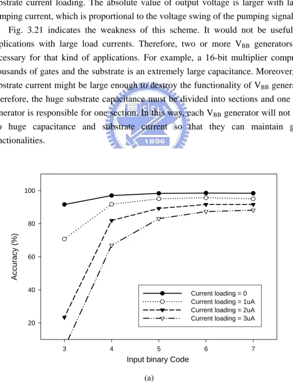
3.2.3 Pumping Current (ICP) and Substrate Current (IBB)……… 37
3.3 Configurable Multiple-Voltage Generators………. 37
3.3.1 Overview of Configurable Scheme………. 38
3.3.1.1 Ring Oscillator……… 38 3.3.1.2 D/A Converter………. 39 3.3.1.3 Code Converter………... 40 3.3.1.4 Initial Control……….. 40 3.3.1.5 Charge Pump………... 41 3.3.1.6 Recovery Circuit………. 41
3.3.2 Output Voltage Equations………... 42
3.4 Simulation Results……….. 42
3.4.1 Transient Waveforms……….. 43
3.4.2 Accuracy Versus Current Loading……….. 44
3.4.3 Operation at Low Supply Voltages………. 45
3.5 Conclusion……….. 46
Chapter 4 Variable-Threshold CMOS (VTCMOS) SRAM Cell Arrays With On-Chip Body-Bias generators……….. 47
4.1 Variable-Threshold CMOS SRAM………. 48
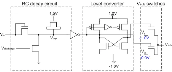
4.1.1 Dynamic Leakage Cut-off Scheme………. 48
4.1.2 Preactivating Mechanism for VTCMOS Cache……….. 49
4.1.3 Auto-Backgate-Controlled MT-CMOS………... 50
4.1.5 Forward Body-Biased SRAM………. 54
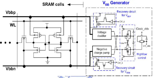
4.2 SRAM Cell Arrays With On-Chip VBB Generators……… 55
4.2.1 On-Chip Dual-Level VBB Generator………... 56
4.2.1.1 Substrate Bias Generator……… 56
4.2.1.2 High/Low Control……….. 56
4.2.1.3 Recovery Circuits……… 57
4.2.2 Simulation Results……….. 57
4.2.2.1 Waveform of VBB Generator………... 58
4.2.2.2 Average Power of VBB Generator……… 58
4.2.2.3 Net Power Saving of SRAM………... 59
4.2.2.4 Composition of Power Sources……….. 61
4.2.2.5 RBB VBBN or VBBP Alone……… 61
4.2.3 Triple-Well Layout for SRAM Cells and VBB Generator………… 63
4.3 Time-Out-Policy VBB Generator Controller……… 64
4.3.1 Schematic Diagram………. 64
4.3.2 Pulse Generator………... 65
4.3.3 State Machine……….. 65
4.3.4 Time-Out Value……….. 67
4.3.5 Simulated Waveforms………. 68
4.3.6 Power Reduction Due to Power-Gating……….. 68
4.4 Conclusion……….. 69
Chapter 5 Power-Gating Technique In Ultra-Low Power SRAM Cell Array Design………. 70
5.1 Stacking Effect……… 70
5.1.1 Self-Reverse Biasing………... 70
5.1.2 Tradeoff Between Delay and Leakage……… 71
5.2 Gated-VDD SRAM Cell………... 72
5.2.1 Virtual GND Node Fluctuation………... 72
5.2.2 Stability/Static Noise Margin……….. 72
5.2.3 SNM Issue of Gated-VDD SRAM Cell……… 73
5.3 Gate Leakage Reduction………. 74
5.4 NMOS or PMOS Gating Device……… 75
5.5 Gated-VDD SRAM Architectures……… 76
5.5.1 Row (Wordline)-Controlled Architecture………... 76
5.5.2 Column-Controlled Architecture………. 77
5.6 Column/Row Co-Controlled Architecture……….. 78
5.6.1 Schematic Diagram………. 78
5.7 Three Typical Schemes for Comparison………. 80
5.7.1 Read-Out Delay………... 80
5.7.2 Cell Standby Power………. 81
5.7.3 Active Power………... 83
5.7.4 Wordline Length, Block Size, and Cell Active Power……… 83
5.7.5 Reduction of Wordline Loading……….. 85
5.7.6 Power-Delay Product……….. 86
5.7.7 Signal Routing and Device Allocation for SRAM Layout………. 87
5.7.8 Area Overhead Due to Extra Devices………. 88
5.8 Conclusion……….. 90
Chapter 6 Conclusions………. 91
References ………. 93
Vita ………. 100
List of Figures
Fig. 2.1 Leakage sources in a MOS device……….. 4
Fig. 2.2 The trend of standby current of MOSFETs………. 5
Fig. 2.3 ION/IOFF and Vt scaling for sub-130nm generations……… 6
Fig. 2.4 Fluctuation of frequency and leakage for dies on a single wafer… 7 Fig. 2.5 Die-to-die Vt and standby leakage variations………. 8
Fig. 2.6 Die-to-die Vt and standby leakage variations………. 9
Fig. 2.7 Operating speed increases with forward body bias………. 10
Fig. 2.8 Characteristics of leakage sources with reversed body-bias……... 11
Fig. 2.9 Block diagram of Self-Adjusting Vt Scheme (SATS)……… 12
Fig. 2.10 Leakage sensor for detecting leakage current of a NMOS transistor……….. 12
Fig. 2.11 Variable threshold-voltage (VT) scheme……… 13
Fig. 2.12 Block diagram of VT circuit………... 14
Fig. 2.13 Schematic of leakage current monitor……… 14
Fig. 2.14 Concept of speed adaptive Vt scheme……… 15
Fig. 2.15 Schematic diagram of Vt-hopping scheme………. 15
Fig. 2.16 Auto body bias generator based on DLL and critical path replica.. 16
Fig. 2.17 Schematic diagram of adaptive body bias generator and the target design………... 17
Fig. 2.18 Schematic diagram of SPR circuit……….. 18
Fig. 2.19 Schematic diagram of self-adjusted FBB scheme……….. 19
Fig. 2.20 The design that using central and local body bias generators to apply FBB………... 20
Fig. 2.21 Schematic diagram of CBG and LBG………. 20
Fig. 2.22 PMOS/NMOS Vt matching scheme………... 21
Fig. 2.23 Operating waveforms of Vt matching scheme……… 22
Fig. 2.24 A possible solution of PMU……… 23
Fig. 2.25 Multiple on-chip Voltage Islands……… 24
Fig. 2.26 A Vt management scheme using programmable status table……. 25
Fig. 2.27 Execution circuit to control power and frequency……….. 26
Fig. 3.1 Internal supply voltages for modern DRAM……….. 27
Fig. 3.2 Cross-section view of triple-well technology………. 28
Fig. 3.3 Dickson charge pump……….. 28
Fig. 3.4 Abstract behavior of Dickson charge pump……… 30
Fig. 3.6 A four-stage charge pump………... 32
Fig. 3.7 Cross-coupled voltage doubler……… 33
Fig. 3.8 Charge pump with PMOS bias……… 33
Fig. 3.9 Voltage doubler with series switches……….. 33
Fig. 3.10 (a) NMOS system and (b) PMOS system………... 34
Fig. 3.11 Hybrid pumping circuit (HPC)………... 35
Fig. 3.12 Cross-coupled hybrid pumping circuit……… 36
Fig. 3.13 Simulated waveforms for the charge pumps………... 36
Fig. 3.14 The mechanism of hot-carrier injection……….. 37
Fig. 3.15 Configurable scheme for multi-voltage generator……….. 38
Fig. 3.16 The ring oscillator with enable control………... 39
Fig. 3.17 (a) The charge-redistribution D/A converter in [3.26] (b) The modified circuit to prevent from Vt loss. (c) The output waveforms……….. 39
Fig. 3.18 The initial control to initialize the D/A converters………. 41
Fig. 3.19 Recovery circuits (a) for VBBN and (b) for VBBP……… 42
Fig. 3.20 Output transient waveforms of the VBB generators (a) for VBBN and (b) for VBBP………. 43
Fig. 3.21 Accuracy versus current loading (a) for VBBN and (b) for VBBP…… 45
Fig. 3.22 Operations under different supply voltages……… 46
Fig. 4.1 Leakage currents and standby currents equations in a SRAM cell ………. 47
Fig. 4.2 (a) Dynamic leakage cut-off SRAM, (b) operating waveforms, well bias drivers for (c) n-well and (d) for p-well……….. 49
Fig. 4.3 Preactivating mechanism for a VTCMOS cache……… 50
Fig. 4.4 Processor organization with a preactivating DLC cache………… 50
Fig. 4.5 Concept of ABC-MT-CMOS……….. 51
Fig. 4.6 Configuration of ABC-MT-CMOS………. 51
Fig. 4.7 Schematic of a dynamic Vt SRAM set………... 52
Fig. 4.8 Schematic of the Vt control circuit using capacitor discharging scheme………. 53
Fig. 4.9 Operating waveforms for Vt control circuit……… 53
Fig. 4.10 Schematic diagram of forward body-biased SRAM………... 55
Fig. 4.11 Operating waveforms of FBB SRAM……… 55
Fig. 4.12 Schematic diagram of SRAM cells with on-chip dual-level VBB generator………. 56
Fig. 4.13 Schematic of high/low control and operating waveforms……….. 57
Fig. 4.15 Simulated waveforms of VBB generator……….. 58
Fig. 4.16 Average power of VBB generator versus time………. 59
Fig. 4.17 Net power saving of SRAM versus time period in standby mode.. 60
Fig. 4.18 Composition of power sources……… 60
Fig. 4.19 Fraction of power overhead for different wordline lengths……… 61
Fig. 4.20 Effectiveness of net power saving for VBBN or VBBP alone………. 62
Fig. 4.21 Power information for VBBN or VBBP alone……… 62
Fig. 4.22 Layout of conventional and triple-well SRAM cells……….. 63
Fig. 4.23 Layout and configuration of triple-well SRAM rows with a VBB generator………... 64
Fig. 4.24 Schematic diagram of VBB generator controller………. 65
Fig. 4.25 Pulse generator and operating waveforms……….. 65
Fig. 4.26 Schematic diagram of state machine………... 66
Fig. 4.27 Schematic of flip-flop with reset signal WL………... 66
Fig. 4.28 State graph of state machine………... 66
Fig. 4.29 Two extreme conditions for defining the time-out value………… 67
Fig. 4.30 Simulated waveforms of VBB generator controller………. 68
Fig. 4.31 Power comparison between with and without power-down scheme………. 69
Fig. 5.1 Stacking effect due to self-reverse biasing of transistor M21………… 70
Fig. 5.2 Using a stacked inverter to observe the tradeoff of delay and leakage current……… 71
Fig. 5.3 Delay-leakage tradeoff of stacking effect………... 71
Fig. 5.4 Gated-VDD SRAM cells (a) without diode and (b) with diode…... 72
Fig. 5.5 Voltage of virtual GND increases after turning off gating device... 73
Fig. 5.6 (a) A latch with static noise sources and (b) Static noise margin… 73 Fig. 5.7 Circuit used to observe the SNM of gated-VDD SRAM cell……... 74
Fig. 5.8 SNM versus scale factor n……….. 74
Fig. 5.9 Gate leakage components and extra leakage currents in gated-VDD SRAM cell………. 75
Fig. 5.10 Dominant leakage sources in an inactive SRAM cell………. 76
Fig. 5.11 Row-controlled SRAM architecture that row decoder controls the gating devices……….. 77
Fig. 5.12 Column-controlled SRAM architecture that column decoder controls the gating devices……….. 78
Fig. 5.13 Proposed column/row co-controlled SRAM scheme……….. 79
Fig. 5.14 Test circuit to observe the cell current in standby and active modes……….. 80
Fig. 5.15 Three SRAM test circuits to compare their performance and
power consumption………. 81
Fig. 5.16 Simulated read-out delay for the three test circuits……… 82
Fig. 5.17 Cell standby power comparison……….. 82
Fig. 5.18 Cell active power comparison………. 83
Fig. 5.19 Cell active power versus different wordline lengths and block sizes………. 84
Fig. 5.20 Cell active power saving versus different wordlines and block sizes………. 84
Fig. 5.21 Simulated waveforms of wordline curves………... 86
Fig. 5.22 Power-delay product………... 86
Fig. 5.23 (a) Layout and (b) allocation of AND gates and gating devices and (c) a wordline with four blocks……… 87
Fig. 5.24 Layout and signal routing of 8Kb SRAM cell arrays………. 88
Fig. 5.25 Area comparison of conventional and new scheme with different block sizes………... 89
Fig. 5.26 Summary of area overhead………. 90
List of Tables
Table 3.1 A 3-bit binary-to-thermometer conversion………. 40 Table 5.1 Cell current in standby and active modes………... 80 Table 5.2 Statistic of 64-bit wordline loading for different schemes……….. 85
Chapter 1
Introduction
In recent years, portable devices and wireless applications are getting popular, such as cell phones, PDAs, and portable computers. It’s emergent to increase battery life and make chips consume as less energy as possible. For the future integrated-circuit (IC) and System-on-Chip (SoC) designs, high-performance operation and low power consumption must be achieved at the same time. Not only the increase of battery life, low-power designs diminish the risks of hot spots and thermal runaway problems. The giga-Hertz operating frequency dramatically increases the temperature and thus degrades the performance. Moreover, the unbalanced temperature distribution across the whole chip causes performance and power fluctuations [1.1], [1.2].
As the technology scales down to deep-submicron and nano-scale eras, both supply voltage (VDD) and threshold voltage (Vt) are reduced for high-performance
and low-power designs. The dynamic power is well known the dominant power component in digital circuits, and the reduction of supply voltage reaches a significant percentage of total power saving. However, the standby leakage cannot be ignored in deep-submicron and nano-scale technologies. In deep-submicron technologies, subthreshold leakage is the critical component among all the leakage currents. Subthreshold leakage increases due to the reduction of threshold voltage with the scaling of technology. In order to compensate the performance degradation of descending supply voltage, threshold voltage is scaled down to satisfy speed requirement. Therefore, the influence of leakage power is becoming significant if threshold voltage keeps on scaling down. One more leakage source called gate-tunneling leakage (or gate leakage) is becoming important in nano-scale technologies. The increase of gate-tunneling leakage is mainly due to the scaling of thickness of gate oxide. Many predictions show that gate leakage has the potential to exceed subthreshold leakage and dominate the standby leakage current in the future [1.3], [1.4]. More seriously, the total standby leakage current may even exceed the dynamic power and dominate the total power consumption. Therefore, this thesis focuses on the techniques for power reduction and leakage currents suppression and applies to SRAM cell array design.
The principles of low-power designs and leakage currents suppression are described in Chapter 2. The detail characteristics and scaling trend of leakage currents in future technologies are discussed. The impacts of parameter variations on performance and power distribution are also mentioned in this chapter. Body biasing is a popular technique to control and eliminate the influences on performance and
power fluctuations. Forward body-bias is applied to low-performance circuits since threshold voltage is reduced. On the other hand, reversed body-bias that raises threshold voltage can be applied to leaky circuits for leakage suppression. Some circuit-level and system-level leakage control techniques will be discussed in the rest of Chapter 2, including the role of power management unit (PMU) and the concepts of Voltage Island techniques.
On-chip voltage generators and configurable body-bias generator design are discussed in Chapter 3. In VLSI and SoC designs, various voltage levels are required for distinct functional blocks. This chapter focuses on the designs of body-bias generators that can reversely bias the substrate of transistors. Charge pumps are popular circuits for generating voltages below GND for NMOS and voltages beyond VDD for PMOS. Moreover, a configurable scheme that can produce various voltage
levels according to control signals is proposed.
In Chapter 4, a dual-level body-biasing generator is proposed and applied to the design of SRAM cell arrays. Many similar designs have been realized before and will be compared in this chapter. However, almost all of these prior designs used external voltage sources instead of on-chip voltage generators. Therefore, the design of SRAM cell arrays adopting on-chip body-bias generators is implemented in this chapter. Finally, a time-out-policy controller for body-bias generator is also presented.
The design of SRAM cell arrays using power-gating technique is realized in Chapter 5. Power gating is an effective technique to suppress leakage current in standby mode by isolating power lines and idle circuits. Attention must be paid to power-gated SRAM cell array designs since data must be retained. Some prior power-gated SRAM architectures are introduced in this chapter. Moreover, a novel architecture that achieves both active and standby power savings is proposed and realized. This architecture induces performance and area overheads, but the power-delay product comparison demonstrates that these overheads are insignificant. Finally, the overall investigation results will be presented in Chapter 6.
Chapter 2
Overview of Low Power Design and Leakage
Control Techniques
In modern digital CMOS integrated circuits, power consumption can be classified into three different components: dynamic, short circuit, and leakage power. Dynamic power is the dominant component of power consumption and results from the charging and discharging of capacitances. Short circuit currents occur when both NMOS and PMOS devices are ON during switching transients. The third component is leakage power. Leakage power is small in comparison with dynamic power, but it’s becoming important in the future deep-submicron and nano-scale technologies and it has the potential to exceed dynamic power [2.1].
In Sec. 2.1, the three components of power consumption will be described briefly. Next, the impacts on performance and power distribution due to process, supply voltage, and temperature variations are discussed in Sec. 2.2. The effects of applying body-bias are described in Sec. 2.2 as well. Besides, some threshold-controlled techniques and novel circuits are presented in Sec. 2.3. Finally, the concepts of Voltage Islands and system-level power control issues are described in Sec. 2.4.
2.1 Power Sources in Digital CMOS Circuits
Dynamic, short circuit, and leakage power are the three major components of digital CMOS integrated circuits.
2.1.1 Dynamic Power
Among the three components of power sources, dynamic power is the dominant component and results from the charging and discharging of capacitances. Dynamic power is given by
2
dynamic switched DD clk
P
=
C
V
f
(2.1)where Cswitched is the total effective switched capacitance, VDD is the supply voltage,
and
f
clk is the switching frequency. It’s obvious that to scale down VDD is the mostefficient way to reduce dynamic power. However, VDD cannot be scaled down forever
2.1.2 Short-Circuit Power
The second component of power consumption is short-circuit power, which results from non-zero rise and fall times of the input waveforms. The non-zero input rise and fall times cause a direct path between VDD and GND for a short time period
during switching. Short-circuit power can be expressed as
2
short circuit sc DD peak clk sc DD clk
P
−=
t V
I
f
=
C V
f
(2.2)where tsc represents the time that the direct path is conducting. Short-circuit power is
proportional to the switching activity, as similar to the dynamic power.
2.1.3 Leakage Power
The third component is leakage power. Leakage current can be divided into many sources, such as subthreshold, band-to-band tunneling, gate tunneling, pn junction reverse bias, DIBL, GIDL, and punchthrough leakage. Fig. 2.1 illustrates these leakage sources in a MOS device.
Among the various leakage sources, subthreshold leakage is the dominant component that is given as
0 0 exp( ) (1 exp ) G T DS DS leakage thermal thermal V Vs V Vs V V I I nV V γ η − − − + − = i − (2.3)
where Vthermal is the thermal voltage, n is the subthreshold swing coefficient constant,
γ is the linearized body effect coefficient, and η is the DIBL coefficient. Assuming that VDS >> Vthermal and (2.2) can be simplified to the expression
0
10
( GS ) / thermal lnleakage
V Vt nV
I
=
I
⋅
− 10 (2.4)Eq. (2.4) implies that subthreshold leakage is smaller with higher threshold voltage, Vt, and this component is becoming important since threshold voltage is scaled down with the progress of CMOS technology.
Subthreshold leakage is becoming the dominant component of power consumption in deep-submicron technologies. However, as the process steps into the region of nano-scale technologies, gate leakage has the potential to dominate the leakage current or even exceed the level of dynamic power. Gate leakage is given as
3 / 2 2 [1 (1 ) ] exp{ } ox ox DT ox ox V B J AE E φ − − = − (2.5) * 3 / 2 3 2 4 2 , 16 3 ox ox m q A B q φ π φ = = (2.6)
where Vox is the voltage drop across the oxide, φox is the barrier height in the conduction band, and is the field across the oxide. In detail, the gate leakage is composed of I
ox E
gd, the gate leakage between gate and drain, Igb between gate and body,
and Igs between gate and source. Fig. 2.2 predicts that gate leakage is indispensable in
nano-scale technologies and the amount of gate leakage is far beyond the standby power constraint. Gate leakage becomes critical due to the decrease of thickness of gate oxide.
Fig. 2.2 The trend of standby current of MOSFETs.
Fig. 2.3 plots the ION/IOFF ratio and Vt for both low and high Vt NMOS
transistors for 130nm, 100nm, and 70nm technologies [2.2], where ION means driving
current in active mode and IOFF stands for leakage current in standby mode. Fig. 2.3
reveals that the leakage current is increasing by 3-5x per generation and becoming comparable with active driving current. The extra leakage current wastes a significant amount of power and causes thermal hot spots and thermal run away problems.
Fig. 2.3 ION/IOFF and Vt scaling for sub-130nm generations.
2.2 Parameter Variations
variations in process, supply voltage, and temperature (P, V, T) are becoming a major challenge in designing future high-performance processors. In the past, CMOS technology variations are mainly due to imperfect process control. However, in present and future devices, intrinsic atomistic variations are becoming very important and cause uncertainty in I-V curves, in timing, and in power dissipation.
Process variations impact the frequency and leakage contribution of chips, causing die-to-die and within-die performance and power fluctuations. In addition, the demand for low power and low supply voltage making voltage variation a significant influence. Above-mentioned variations make some dies on a single wafer cannot achieve the target frequency, while some others fail to satisfy the leakage power constraint.
2.2.1 Process Variations
Fig. 2.3 plots the frequency and leakage distributions of dies on a signal wafer [2.3]. Due to both die-to-die and within-die parameter variations, significant variation exists in frequency and leakage power. At the same time, accepted dies must meet the frequency and leakage constraints. Notice that most of the ultra-high speed dies consume too large leakage power and they must be discarded. The ultra-low speed dies that have reasonably high leakage must be discarded as well since they cannot achieve the performance requirement.
Fig. 2.4 Fluctuation of frequency and leakage for dies on a single wafer.
The wide leakage or standby current distribution comes from channel length and threshold voltage (Vt) variations, as illustrated in Fig. 2.2. The fluctuation of Vt among the dies results in wide spread of leakage current.
Fig. 2.5 Die-to-die Vt and standby leakage variations.
2.2.2 Supply Voltage Variations
Differences of switching activity and logic circuits across the die cause uneven power dissipation in the die. Thus, uneven supply voltage distribution and temperature hot spots occur and lead to variation of subthreshold leakage across the die. The scaling of supply voltage due to technology progress degrades this effect since the impact on supply voltage is relatively larger.
2.2.3 Temperature Variations
As described previously, differences of switching activity and types of logic across the die cause uneven power dissipation in the die. Therefore, different thermal distributions appear in the distinct parts of the die and result in variations of leakage. The measurement results in [2.4] demonstrate that the standby leakage current increases with the increase of temperature. Not only the increase of standby leakage current, a high temperature further degrades the performance of devices.
2.2.4 Applying Body-Bias for Reducing Parameter Variations
The leakage and frequency on a single die can be controlled through body bias. The leakage current can be significantly reduced by applying reversed body-bias (RBB) due to the increase of threshold voltage. On the other hand, by applying forward body-bias (FBB) the threshold voltage is lowered down and thus the speed is improved.
Fig. 2.6 shows that the leakage current decreases with applied reversed boy-bias due to the increase of threshold voltage [2.5]. RBB can be applied to the dies on a single wafer that are too leaky for suppressing leakage current. Besides, RBB can be applied to circuit blocks on a single die that are too leaky for compensating within-die leakage fluctuation. However, the performance degradation due to RBB must be taken into account.
Fig. 2.6 Die-to-die Vt and standby leakage variations.
2.2.4.2 Forward Body-Bias for Improving Performance
By applying forward body-bias the operating speed is improved due to the decrease of threshold voltage, as shown in Fig. 2.7 [2.6]. Since the threshold voltage is decreased, thus the active driving current increases to speedup the operation. Therefore, FBB is beneficial to dies on a single wafer or circuit blocks on a single die that fail to achieve required performance. However, the induced extra leakage current is an issue that one must pay attention to it.
Fig. 2.7 Operating speed increases with forward body bias.
2.2.5 Effectiveness and Optimum Value of Reversed Body-Bias
From the previous description it has been seen that applying RBB is an effective and widely used technique to reduce leakage current. Unfortunately, the effectiveness degrades in advanced technologies. [2.5] shows that the intrinsic leakage current increases with the decrease of channel length. In addition, the effectiveness of applying RBB at nominal transistor channel lengths (Lnom) is better than shorter channel lengths condition (Lwc). Because of worsening short channel effect (SCE), effectiveness of RBB diminishes with technology scaling. This means that to keep SCE under control becomes more important as the technology scales down. Another reasons is the growing gate leakage, which is immune to RBB.
Many researches and measurements have shown that an optimum RBB value exists which is different from different technologies [2.7], [2.8], [2.9]. Biasing in the optimum RBB condition a least leakage power is consumed, and leakage power increases when the applied RBB exceeds the optimum value. One reason is that the band-to-band tunneling leakage increases due to RBB [2.10]. Fig. 2.8 illustrates the characteristics of leakage sources with RBB [2.2] and shows that GIDL increases with RBB. Obviously, an optimum RBB value exists and a least leakage power is achieved in this condition.
Fig. 2.8 Characteristics of leakage sources with reversed body-bias.
2.3 Design Techniques for Controlling Threshold Voltage
The most popular technique for controlling threshold voltage is applying body bias. Threshold voltage is raised with RBB, while threshold voltage is lowered with FBB. In this section, many designs and techniques for controlling threshold voltage are introduced, including RBB and FBB control methodologies. Beside, one more matching circuit for balancing threshold voltage of NMOS and PMOS is also described.
2.3.1 Adaptive Variable Threshold Voltage Techniques
Here some circuit techniques for dynamically varying threshold voltage are introduced. The threshold voltage is adaptively adjusted in real time according to operating speed or leakage current.
2.3.1.1 Self-Adjusting Threshold-Voltage Scheme
A circuit technique called Self-Adjusting Threshold-Voltage Scheme (SATS) is to reduce the Vt fluctuation by using self-substrate-biasing [2.11]. The SATS comprises a leakage sensor and a self-substrate-bias circuit (SSB). The leakage sensor detects the leakage current of the design and controls SSB.
Fig. 2.9 shows the block diagram of the SATS to reduce the Vt fluctuation. A leakage sensor detects leakage current of a representative MOS transistor and sends a control signal, Vcont, to SSB. Vcont triggers SSB only when the leakage is higher than a predetermined level. That is, Vt is set to the lowest value that satisfies the power
specification. However, the tradeoff between leakage current and operating speed must be considered carefully.
Fig. 2.9 Block diagram of Self-Adjusting Vt Scheme (SATS).
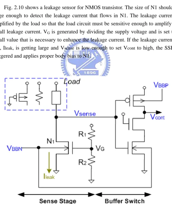
Fig. 2.10 shows a leakage sensor for NMOS transistor. The size of N1 should be large enough to detect the leakage current that flows in N1. The leakage current is amplified by the load so that the load circuit must be sensitive enough to amplify the small leakage current. VG is generated by dividing the supply voltage and is set to a
small value that is necessary to enhance the leakage current. If the leakage current of N1, Ileak, is getting large and Vsense is low enough to set Vcont to high, the SSB is triggered and applies proper body bias to N1.
2.3.1.2 Variable Threshold-Voltage Scheme
Fig. 2.11 illustrates the Variable Threshold-voltage (VT) scheme [2.12] and the threshold voltage of a transistor is controlled through a Variable Threshold-voltage circuit (VT circuit). The VT circuit controls VBB to compensate the Vt fluctuation in
the active mode. In the standby mode, the VT circuit applies deeper RBB to increase Vt and thus reduce leakage current.
Fig. 2.11 Variable threshold-voltage (VT) scheme.
As depicted in Fig. 2.12, the VT circuit consists of four leakage current monitors (LCM’s), a self-substrate bias circuit (SSB), and a substrate charge injector (SCI). The SSB is used to lower the voltage of VBB, while the SCI injects charges into the
substrate to raise VBB. The monitors that detect the level of VBB control the operations
of both the SSB and SCI.
Fig. 2.13 shows the schematic of LCM and the connections between SSB and DCT core. The LCM detects the leakage current of DCT core, Ileak, DCT, through the
transistor M4 that shares the same substrate with the DCT. If Ileak, LCM is larger than a
predetermined level, the node N1 goes low and force Nout to go high to activate SSB.
Consequently, the VBB becomes deeper and Ileak, LCM and Ileak, DCT become smaller. It’s
undoubtedly that the SSB is disabled when Ileak, LCM is still under the predetermined
Fig. 2.12 Block diagram of VT circuit.
Fig. 2.13 Schematic of leakage current monitor.
2.3.1.3 Speed-Adaptive Threshold-Voltage Scheme
A speed adaptive threshold-voltage (SA-Vt) scheme is illustrated in Fig. 2.14 [2.13]. It consists of a delay line, a delay comparator, a decoder, and VBB generators.
The propagation delay of delay line is controlled by varying the substrate voltage of delay line. If the speed of the delay line changes, the comparator detects and recognizes whether the speed is slower or faster. Then, the comparator sends signals to the decoder, and the decoder controls the VBB generators so that proper VBN and
VBP are produced.
The delay line is simply an inverter chain, and the comparator can be implemented with a phase detector. Basically, the concept of SA-Vt scheme is like phase-locked loop (PLL) or delay-locked loop (DLL), but the difference is that SA-Vt scheme dynamically varies the substrate bias of delay line.
Fig. 2.14 Concept of speed adaptive Vt scheme.
2.3.1.4 Software-Controlled Vt-Hopping Scheme
Fig. 2.15 shows the Vt-hopping scheme that the substrate bias is dynamically controlled by software [2.14]. The power control block generates select signals, Vt_low_enable, and Vt_high_enable, according to the control signal, CONT. Note that CONT comes from the processor. The threshold voltage of the processor is higher if Vt_high_enable is asserted, while the threshold voltage is lower if Vt_low_enable is asserted.
Signal CONT is also used to control the operating frequency of the processor. When Vt_low_enable is high, the frequency controller feeds fclk to the processor. On
the other hand, when Vt_high_enable is asserted, the frequency controller generates fclk /2 to the processor. Besides, more than two sets of frequency and threshold voltage
can be extended if necessary.
The required maximum operating frequency determines the value of the lower threshold voltage. The processor must achieve fclk with the lower threshold voltage,
while fclk /2 must be achieved with the higher threshold voltage.
2.3.1.5 Automatic Supply Voltage and Body Bias Scheme
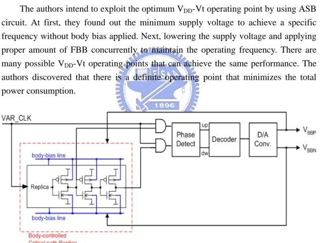
An adaptive supply voltage and body bias (ASB) scheme has been developed to exploit the optimum operating condition that least active power is consumed [2.15]. Fig. 2.16 illustrates the schematic diagram of ASB, which is based on DLL and critical path replica. The ASB scheme uses a DLL to adjust the body bias values until the speed of the critical path replica equals the target frequency exactly. The critical path replica must closely track the performance of the actual critical path of a design as supply and body voltages vary.
The authors intend to exploit the optimum VDD-Vt operating point by using ASB
circuit. At first, they found out the minimum supply voltage to achieve a specific frequency without body bias applied. Next, lowering the supply voltage and applying proper amount of FBB concurrently to maintain the operating frequency. There are many possible VDD-Vt operating points that can achieve the same performance. The
authors discovered that there is a definite operating point that minimizes the total power consumption.
Fig. 2.16 Auto body bias generator based on DLL and critical path replica.
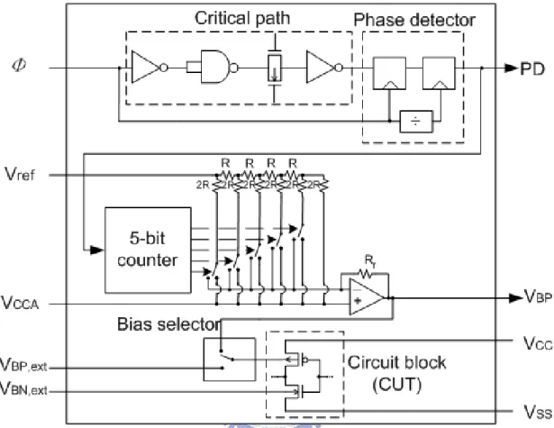
2.3.1.6 Digital Control in Adaptive Body Bias
A bidirectional adaptive body bias (ABB) generator has been developed to apply RBB for low leakage and FBB for high performance, as in Fig. 2.17 [2.16]. The authors used ABB to reduce the impacts of die-to-die and within-die parameter
variations. That is, proper FBB is applied to the dies that are below the frequency constraint, and proper RBB is applied to the dies that consume too much leakage power.
Fig. 2.17 Schematic diagram of adaptive body bias generator and the target design.
ABB circuit comprises a critical path replica, a phase detector, a 5-bit counter, and a resistor network with an amplifier. The critical path replica can be constructed by a ring-oscillator structure for measuring the operating frequency. The phase detector compares the critical path delay with the target clock period and sends control signals to the counter. The counter receives signals from the phase detector and controls the resistor network. The resistor network and the amplifier can be seen as a D/A converter that produces body bias to the substrate of PMOS. Therefore, the body bias voltage can be configured digitally through the counter.
2.3.2 Dynamic Threshold Voltage Techniques
In contrast to the adaptive variable threshold-voltage techniques described previously, dynamic threshold-voltage techniques here without sensors and adjust threshold voltage dynamically according to mode control signals. In addition, their
FBB or RBB values are fixed and one bias level is for one operating mode.
2.3.2.1 Standby Power Reduction Circuit
Fig. 2.18 depicts a standby power reduction (SPR) scheme that switches the voltages of n-well and p-well in different operating modes [2.17]. The SPR circuit consists of a level shifter and a voltage switch.
Fig. 2.18 Schematic diagram of SPR circuit.
In the active mode CE is asserted, and VPWELL and VNWELL are switched to 0V
and 2V, respectively. In the active mode zero body bias (ZBB) is applied and high performance is maintained. When CE is pulled low in standby mode, VPWELL and
VNWELL are switched to -2V and 4V, respectively. In the standby mode RBB is applied
and standby leakage is significantly reduced.
It’s remarkable that four external power sources are needed, VNBB, VDD, VSS, and
VPBB. However, the operations of this scheme are questionable if VNBB and VPBB are
generated by charge pump circuits. Assume that VNBB and VPBB come from charge
pump circuits and VSS and VDD are external power sources, the voltage levels of VNBB
and VPBB will be influenced during the switching activities. This is because of the
2.3.2.2 Self-Adjusted Forward Body Bias
Fig. 2.19 shows a technique called self-adjusted forward body bias (SAFBB) that adopts current sources to bias the substrate nodes [2.11]. The purpose of this scheme is to achieve high performance with a low supply voltage and thus low active power.
The signals Cbn and Cbp control the body bias depending on the condition of the
target design. Cbn is pulled low and Cbp is pulled high in the standby mode, thus ZBB
is applied. When in the active mode, Cbn is pulled high and Cbp is pulled low and FBB
is applied to the substrate nodes. The amount of applied FBB can be varied by carefully designing the current sources.
Fig. 2.19 Schematic diagram of self-adjusted FBB scheme.
2.3.2.3 Central and Local Body Bias Generators
A design that uses central and local body bias generators is depicted in Fig. 2.20 [2.18], which applies FBB to the PMOS transistors of the target core circuit. Note that only one central bias generator (CBG) is constructed, but many local bias generators (LBG) are necessary to drive many macros.
The CBG uses a scaled bandgap circuit to generate a process, voltage, and temperature-invariant reference voltage, and then this voltage is routed to all of the LBGs. The reference voltage is about 450mV below the bandgap supply VCCA, and
this means that the amount of FBB applied is about 450mV. The LBG is used to translate the reference voltage to a body bias voltage that is referenced to the local supply VCC.
Fig. 2.20 The design that using central and local body bias generators to apply FBB.
Fig. 2.21 shows the schematic of CBG and LBG. The usage of separate CBG and LBG ensures that any variations in the local supply voltage VCC will be tracked by the
body voltage and thus a constant FBB of 450mV is maintained. Translation of the reference voltage is realized through a current mirror followed by a voltage driver, which is to drive the final n-well load. FBB is applied to the target design in the active mode, while ZBB is applied in the standby mode by switching on the zero-bias switch.
2.3.3 Threshold Voltage Matching Scheme
For low-power and low-voltage system, the fluctuation of performance is becoming a critical issue. The variations of process, supply voltage, and temperature are major sources of fluctuations of performance. As the technologies scale down, the supply voltage and threshold voltage are lower so that the variations of supply voltage and threshold voltage are becoming more serious. Moreover, the Vt difference between PMOS and NMOS degrades the performance and operating margin of chips. Since Vt is getting smaller in advanced technologies, a small variation of Vt can significantly impact the performance and reliability.
Fig. 2.22 PMOS/NMOS Vt matching scheme.
Fig. 2.22 shows a Vt matching scheme that consists of a logical threshold detector, a comparator, a shift register, a NMOS bias generator, and a reference supply [2.19]. The logical threshold detector is composed of a CMOS inverter chain that the input and the output is connected. The logical threshold detector is used to detect Vt unbalance. The comparator detects whether the Vlog level is between Vrefa and Vrefb
and outputs the diff signal to control the NMOS bias generator. The NMOS bias generator varies the bias voltage Vbnlog if the Vlog level is above or below the region
determined by Vrefa and Vrefb.
Fig. 2.23 shows the operating waveforms of Vt matching scheme. As first, the Vlog is beyond the predetermined region due to Vt unbalance. The comparator detects
the unbalance and shift register forces the NMOS bias generator to supply larger Vbnlog. The NMOS bias generator is stopped until the Vlog is within the predetermined
region.
Fig. 2.23 Operating waveforms of Vt matching scheme.
2.4 System-Level Power Control
The previous sections described many circuit-level threshold-voltage control techniques. However, with the progress of semiconductor technology and the trend of System-on-Chip (SoC), a system-level power and performance control methodology is more efficient. In this section, a power management unit (PMU) and its functionalities are introduced. Besides, the concept of Voltage Islands and a power control technique using status table is described.
2.4.1 Overview of PMU
Power management is a real-time technique to dynamically monitor and control power distribution and performance of a chip. Fig. 2.24 shows the block diagram of a possible PMU solution. It’s mainly consists of supply and body-bias voltage generators, device performance and thermal monitors, control logics, clock generators, and state machines. The voltage generators internally supply various voltages to serve as supply voltage or body bias; the monitors observe and detect the device performance and the temperature to keep the functionality and performance. Control logics are used to control the operation modes of functional blocks, and the power management state machine keeps tract of the mode transitions of functional blocks.
Fig. 2.24 A possible solution of PMU.
PMU monitors the power and performance conditions of all functional blocks, and executes operating mode transitions according to the activities. That is, if a functional block is in its high power and performance state but without any task to do, PMU sends control signals to change the power state. In addition, if the thermal detector observes that the temperature of a functional block goes too high, PMU enforces the IP to slow down the operating speed.
2.4.2 Concept of Voltage Islands
Voltage Islands are areas (logic and/or memory) on the same chip that are supplied by different voltage sources [2.20]. As discussed before, the various voltages may come from DC/DC converters. Voltage Islands restore the concept of individual voltage optimization of functional blocks to SoC design. Individual functional blocks of the SoC design can have different power characteristics from the rest of the design, and can be optimized accordingly. For example, the most performance-critical element of the design, such as a processor core, requires the highest voltage to maintain the required high performance. On the other hand, such as memory cells or control logics may not require this level of voltage. Therefore, significant power can be saved if they can run at lower voltages.
Fig. 2.25 Multiple on-chip Voltage Islands.
Fig. 2.25 shows the multiple on-chip Voltage Islands, which are operated under different supply voltages. In general, the circuits in the same Voltage Island have similar operation characteristics. As in Fig. 2.25, for instance, the Voltage Island 2 is a DSP (digital signal processing) processor and it can be fully shut down if we know that there are no DSP operations needed. An effective way is to add gating devices between the processor and the supply voltage or the ground.
Power domains are areas within an Island supplied by the same power supply but have distinct gating devices. According to the operating characteristics, part of an Island can be power gated but others are still power on.
2.4.3 Managing Threshold-Voltage Through a Status Table
A Vt management scheme using programmable status table is illustrated in Fig. 2.26 [2.21]. It consists of an instruction decoder, status monitor, programmable registers, and some logics. The decoder decodes an instructions and the requirement table identifies the function units that are required to execute this instruction. The status table stores the present power status of each function units. The logic observes whether the power requirement and power status are in agreement. If an instruction requires one function unit that is in lower power state, the execute logic sends control signals to change the power state to a higher level. A higher power state means both larger supply voltage and higher operating frequency. On the other hand, if another one function unit that is in higher power state is not required, the execute logic lowers
the supply voltage and frequency or even shuts down the function unit.
The existence of override register allows direct control of power and speed by application software. In other words, the override register can be programmed to directly control the power and speed of function units regardless of the internal managing scheme. For example, a reset signal from software can initialize the tables and put all the function units to the lowest power state.
The power latency table, as the broken-lined square in Fig. 2.26, is included but it does not appear in [2.21]. The power latency table contains the information of time periods required for power state transitions. The time latency of power state transitions must be taken into account since input data should be stalled until the required power state is ready. A false operation results from the execution under incorrect power state.
Fig. 2.26 A Vt management scheme using programmable status table.
2.4.4 Execution Circuit for Power and Performance Transition
Fig. 2.27 shows an execution circuit to adjust the voltage and frequency. Assume that each function unit has dedicated DC/DC converter and body bias generator, which can be independently controlled by PMU. The voltage generators can be shut down if the function unit is inactive. Moreover, the supply voltage and body bias can be dynamically adjusted if the DC/DC converter and body-bias generator are configurable.
Each function unit has a dedicated frequency divider to vary the operating frequency. According to the control signals from PMU, the frequency of function unit can be adjusted through a frequency divider. Undoubtedly, the clock signal fed into function unit can be gated for further power saving.
Fig. 2.27 Execution circuit to control power and frequency.
2.5 Conclusion
The most important leakage sources in deep-submicron and nano-scale CMOS devices are described in Sec. 2.1. Among them, the subthreshold leakage is the most critical portion and can be significantly reduced by raising threshold voltage, Vt. A popular technique for adjusting threshold voltage is to apply body bias. The influences on leakage and performance of applying body bias are also discussed. In Sec. 2.2, the influence of die-to-die and within-die parameter variations are discussed.
Some techniques and circuits for controlling threshold voltage are introduced in Sec. 2.3. Some of them detect and control threshold voltage in real time, and others switch body voltage depending on operating mode. Finally, the concept of PMU and Voltage Islands are described in Sec. 2.4, and a threshold-voltage managing scheme using a status table is introduced.
By applying RBB a significant amount of leakage current can be reduced, while applying FBB can achieve higher performance. However, the extra power and area induced by body-bias generators cannot be ignored. Generally speaking, the power overhead must be less than saved leakage power. In addition, the time latency of charging and discharging substrate nodes is another issue that influences the performance.
Voltage Islands is a system architecture and chip implementation methodology that can dynamically manage power and performance for SoC designs. An Island means the area that is fed by the same supply voltage. The process of functional partitioning identifies the optimal supply voltage of each functional component that minimized active power at the required performance.
Chapter 3
On-Chip Voltage Generators and Configurable
Body-Bias Generator Design
In the past decades, on-chip voltage generators have been widely used in commercial memory chips such as DRAMs and Flash memory [3.1], [3.2], [3.3]. As shown in Fig. 3.1 [3.4], For example, DRAM chips need various kinds of power-supply voltages, which have been generated internally by using single external power supply. This feature is getting more emergent in recent low-power and SoC (System-on-Chip) systems.
Not only the advantages in memory designs, voltage generators are beneficial in other digital ICs as well. In the future low-voltage CMOS IC designs, internally generated voltages will be indispensable to reduce subthreshold current, which exponentially increases with decreasing threshold voltage. Many logic-oriented circuits have adopted this technique to control their threshold voltages [3.5], [3.6], [3.7]. It’s commonly used to dynamically adjust threshold voltage by utilizing body bias in a triple-well technology, as illustrated in Fig. 3.2[3.8]. Obviously, various voltages must be generated internally to meet the requirements, and therefore some on-chip voltage generators are necessary.
As for body bias generators (VBB generators), charge pump based structure is
quite popular, and they can generate voltages that higher than supply voltage (VDD) or
lower than ground (GND). The basic principles of positive-pumping and negative-pumping are described in Sec. 3.1 and Sec. 3.2, respectively. A digital-controlled configurable scheme is discussed in Sec. 3.3 and Sec. 3.4 shows the simulation results. Finally, some conclusions are made in Sec. 3.5.
Fig. 3.2 Cross-section view of triple-well technology.
3.1 Positive-Pumping Circuits
Positive charge pumps are circuits that can pump charges upward to produce voltages higher than the common supply voltage. Those circuits are widely used in non-volatile memories such as EEPROM and Flash memories [3.9]. This section introduces the basic operations of positive-pumping circuits and some advanced positive charge pumps.
3.1.1 Dickson Charge Pump
Most charge pumps are based on the circuit proposed by Dickson [3.10], and the circuit is called “Dickson charge pump”.
3.1.1.1 Overview of Dickson Charge Pump
Fig. 3.3 shows the Dickson charge pump and the MOS transistors act as diodes, so the charges can only be pushed in one way. The circuit is composed of diode-connected MOS transistors and pumping capacitors, Cp. Generally the pumping
capacitors can be replaced with MOS capacitors. The two pumping signals, clk and clk are out of phase and their peak-to-peak swings are both VDD.
3.1.1.2 Operation of Dickson Charge Pump
With the pumping capacitors, the two clocks push the charged nodes upward through the transistors. Each time when the clock signal goes from low to high, the voltage difference (denoted as ΔV) at internal node can be expressed as [3.11]
0 ( ) p DD p s p s C I V V C C f C C ∆ = ⋅ − + ⋅ + (3.1)
where Cs is the parasitic capacitance at each node, f is the pumping frequency, and
I0 is the output current loading. When clk goes from low to high andclkgoes from high to low, the voltage at node 1 is pumped to V1 +ΔV, and the voltage at node 2 is
settled to V2, where V1 and V2 are defined as the steady-state lower voltage at node 1
and node 2, respectively. The voltage pumping gain for second pumping stage is defined as the difference between V2 and V1,
2 1 tn
V −V = ∆ −V V 2 (3.2)
where Vtn2 is the threshold voltage of the second transistor. Therefore, the necessary condition for the circuit to function is thatΔV must greater than the threshold voltage. For an ideal charge pump, the output voltage goes toward [3.12]
( )
out DD t DD
V = V −V ⋅ N +V (3.3)
where N is the number of stages.
3.1.1.3 Limitation of Dickson Charge Pump
From (3.3), it’s obvious that the voltage gain per stage of Dickson charge pump suffers from the threshold voltage losses. Unfortunately, the threshold voltage increases due to body effect, especially at the high-voltage nodes near the output. Therefore, the output voltage of Dickson charge pump cannot be a linear function of the number of stages. Moreover, the pumping efficiency degrades as the number of stages increases. Fig. 3.4 depicts the operation behavior abstractly.
Fig. 3.4 Abstract behavior of Dickson charge pump.
3.1.2 Improvement of Voltage Gain
Due to the threshold voltage loss and the influence of body effect, a large number of researches attempt to alleviate this problem. In order to diminish the threshold voltage loss of conventional charge pump, one replaces most of the NMOSFET’s with PMOSFET’s [3.13]. This circuit achieves high efficiency and pumping speed, but some bootstrapped clock generators are needed. Moreover, it requires four pumping signals so that increases the complexity. On the other hand, using floating-well to eliminate the body effect is proposed [3.14]. However, the substrate currents generated may still reduce the efficiency.
3.1.3 Charge Pump Without Body Effect
From the discussions in the sections above, the main obstacles of charge pumps are the influence of body effect, and the operations under low supply voltage. One proposed a scheme that uses two auxiliary MOSFET’s to control the body bias [3.12]. As in Fig. 3.5, each charge transfer block is composed of three PMOS transistors, where MT is the charge-transfer transistor, and MS and MD are the two auxiliary
transistors. When MT is ON, the charges are transferred through it. Meanwhile, MS is
ON and MD is OFF, the body and source of MT are connected through MS. on the
other hand, when MT is OFF, thus MS is OFF and MD is ON. In this condition the
source and the body of MT are still connected through MD.
In summary, the two auxiliary transistors supply two paths to join the source and the body of MD, one for clk is high and the other for clk is low. In this scheme since
the charge-transfer transistor has zero source-body voltage, therefore it suffers no body effect and achieves higher voltage gain.
Fig. 3.5 The charge pump without body effect.
3.1.4 Charge Pump for Low-Voltage Operation
As discussed before, one major limitation of charge pump is the functional ability under low supply voltage. Fig. 3.6 shows a charge pump using dynamic charge transfer switch and backward control [3.11]. This circuit is suitable for operating under low supply voltages.
In this scheme the single-stage voltage pumping gain is
2 2 1
V V
G = G = V −V = ∆ (3.4) V
When ψ1 is high andψ2 is low, both the voltages at node 1 and node 2 are V2,
and the voltage at node 3 is 2 . In order to function well, the following expression must be satisfied
V ∆
2∆V > Vtp and 2∆V > V Vtn( 2) (3.5)
On the other hand, whenψ1 is low andψ2 is high, the voltage at node 1 is V1,
both the voltages at node 2 and node 3 are 2∆V. It must satisfies
2∆V > V Vtn( 1) (3.6)
In comparison with expressions (3.2), this circuit can achieve the required conditions more easily under low supply voltage.
Fig. 3.6 A four-stage charge pump.
3.1.5 Voltage Doubler
A large amount of voltage multipliers are based on Dickson charge pump, as discussed in the sections above. However, a high voltage can also be achieved by cascading several voltage doublers [3.15]. A voltage doubler can generate twice the magnitude of input voltage. Fig. 3.7 shows the popular cross-coupled structure voltage doubler proposed in [3.16]. This circuit needs a series switch to output the doubled DC voltage.
A scheme uses two charge pump blocks, one for the supply and the other to bias the body of the switch, as shown in Fig. 3.8 [3.17]. Since there are no junction bias between the body and the output, thus no substrate current exists. The disadvantages of Fig. 3.8 are that it requires two equivalent blocks and the body of P2 is still unbiased.
To solve these problems, another design uses a dual series switch and the principle of bulk switching, as depicted in Fig. 3.9 [3.18]. M3 and M4 are series switches, and M5 and M6 switch to the highest voltage. For M3 and M4, their body and the output node and the chip substrate compose of vertical PnP bipolar transistor. Since M5 and M6 switch the bodies of M3 and M4 to the highest voltage, the circuit is latch-up immune.
Fig. 3.7 Cross-coupled voltage doubler.
Fig. 3.8 Charge pump with PMOS bias.
3.2 Negative-pumping circuits
In contrast to positive-pumping circuits, negative-pumping circuits generate voltages lower than ground (potential = 0). The most common usage of negative-pumping circuits is to reversely bias the pn junction between source and body of NMOS transistors and suppress subthreshold leakage current. The body-bias voltage generators have been adopted in memory for a long time. They can stabilize the operations of memory cells and peripheral circuits [3.4]. Not only in memories, they are getting more important in logic designs, especially in nano-scale and SoC eras. In this section, the principles of negative-pumping circuits will be addressed.
3.2.1 Basic Principles of Negative-Pumping Circuits
Fig. 3.10 (a) shows the conventional negative-pumping circuit [3.19]. The circuit comprises two diode-connected NMOS transistors and one capacitor. We can call it NMOS system here. When clk is high, the internal node n1 is pushed upward to Vtn,
the threshold voltage of NMOS. When clk goes low, node n1 is pulled to (–VDD + Vtn1)
and the output node VBB is
1
BB DD tn tn
V = −V + V +V 2 (3.7)
It’s easily understood that the NMOS system suffers from body effect seriously, since VBB becomes shallower with the increases of Vtn1 and Vtn2 due to body effect.
Besides, the minority carrier injection occurs when node n1 goes low, because the n+ regions of Q1 and Q2 are forward biased against the p-well.
Fig. 3.10 (a) NMOS system and (b) PMOS system.
A charge pump that is composed of PMOS transistors called PMOS system is shown in Fig. 3.10 (b). Since node n2 can achieve –VDD, thus output node VBB
reaches
BB DD tp
V = −V + V (3.8) where the Vtp is due to Q1. In comparison with equation (3.8) and (3.7), the PMOS
system generates deeper voltage than NMOS system but still slightly suffers from threshold voltage loss.
3.2.2 No Vt-Loss Pumping Circuits
In contrast to the previous two circuits, in the following two high-performance circuits without Vt-loss are described.
3.2.2.1 Hybrid Pumping Circuit
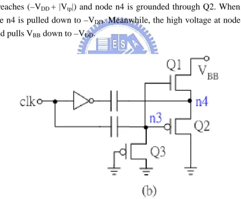
The hybrid pumping circuit (HPC) uses both NMOS and PMOS, as in Fig. 3.11 [3.20]. The most important feature of HPC is the replacement of Q1. When clk is low, node n3 reaches (–VDD + |Vtp|) and node n4 is grounded through Q2. When clk goes
high, node n4 is pulled down to –VDD. Meanwhile, the high voltage at node n3 turns
on Q1, and pulls VBB down to –VDD.
Fig. 3.11 Hybrid pumping circuit (HPC).
3.2.2.2 Cross-Coupled Hybrid Pumping Circuit
Another high performance pumping circuit uses cross-coupled structure to achieve high-speed [3.21], as shown in Fig. 3.12. Because nodes n5 and n6 are cross-coupled, their low voltages are enough to fully turn on MP1 and MP2, respectively.
Fig. 3.12 Cross-coupled hybrid pumping circuit.
3.2.2.3 Simulated Output Waveforms
Fig. 3.13 shows the simulated output waveforms for the previous charge pumps. As described above, NMOS system suffers from two Vt losses and PMOS system suffers from one. On thee other hand, both HPC and cross-coupled HPC are free from body effect so that they can closely reach –VDD.
Time (us) 0 1 2 3 4 V BB (v o lt. ) -1 0 NMOS system PMOS_system HPC Cross-coupled HPC VDD=1.2V -0.5V -0.8V -1.13V -1.17V
![Fig. 2.18 depicts a standby power reduction (SPR) scheme that switches the voltages of n-well and p-well in different operating modes [2.17]](https://thumb-ap.123doks.com/thumbv2/9libinfo/8240315.171306/32.892.142.754.333.746/depicts-standby-reduction-scheme-switches-voltages-different-operating.webp)
![Fig. 4.7 shows a dynamic Vt SRAM to reduce subthreshold leakage current [4.4]. The two NMOS transistors serve as voltage switches to dynamically adjust the voltage of substrate in different operating modes](https://thumb-ap.123doks.com/thumbv2/9libinfo/8240315.171306/66.892.153.741.543.841/dynamic-subthreshold-transistors-switches-dynamically-substrate-different-operating.webp)