Broadband semiconductor optical amplifiers and tunable
semiconductor lasers
a,b,c
Ching-Fuh
Lin, aYi-Shin
Su, aFei-Hung
Chu, and
d Chia-Wei Tsai
a
with
Graduate Institute of Electro-Optical Engineering
b with
Department of Electrical Engineering
C
with
Graduate Institute of Electronics Engineering
d with
Department of Physics
National Taiwan University, Taipei, Taiwan
ABSTRACT
Nonidentical multiple quantum wells (MQWs) had been widely used for broadening the emission or gain bandwidth of semiconductor optical amplifiers (SOAs). However, the carrier distribution among the MQWs is not uniform, leading to
nonuniform gain contributed from different QWs. Thus using nonidentical MQWs for broadband purpose is not
intuitively straightforward. Several factors need to be carefully considered. Those factors include the QW sequence, electron/hole transport time across the separate confinement hetero-structure, as well as carrier capture time. In this work, we will discuss the design of MQWs for broadband SOAs. With properly designed nonidentical MQWs, the emission bandwidth could be nearly 400 nm. Also, the tuning range of semiconductor lasers could be extended to be over 200 nm.
Keywords: semiconductor optical amplifiers, carrier distribution, broadband, nonidentical multiple quantum wells, quantum-well sequence, separate confinement hetero-structure, emission bandwidth
1. INTRODUCTION
Broadband characteristics of semiconductor optical amplifiers (SOAs) and tunable semiconductor lasers are useful for
applications in areas such as optical communication, spectroscopy, and interferemetric tomography. For optical
communication, the optical fiber exhibits very broad bandwidth, almost covering the range from 1 .2 ji m to 1 .6 ji m with
a loss of less than 1dB/km. Optical-fiber communication therefore requires components and systems to have similar
broadband characteristics. However, Er-doped fiber amplifiers and lasers provide a bandwidth much less than the
available range of optical fibers. Semiconductor lasers/amplifiers using multiple-quantum-well (MQW) engineering thus provide another possibility for the broadband purpose. In addition, they are of compact size and can be directly integrated with electronic components, making them more attractive than other types of devices for the same purpose.
Conventional SOAs usually have a bandwidth of less than 5Onm. To cover the entire usable bandwidth of an optical fiber, many conventional SOAs having different spectral ranges are required. If the bandwidth of SOAs could be broadened, they will be even more attractive. Many methods can be used to broaden the bandwidth of SOAs. One is using simultaneous transitions of several quantized levels in a quantum 2However,simultaneous transitions of different quantized levels can occur only when band-filling effect is obvious at high injection current. In addition, the resulting bandwidth highly depends on the device length, which influences the required population for a certain gain or
lasing condition. The other method is to use multiple quantum wells (MQW) of different types. Unfortunately,
carriers mainly populate in certain quantum wells only. The nonuniform carrier distribution leads to the gain bandwidth not contributed from every quantum well '' andso makes the design of multiple quantum wells for broadband purpose not straightforward.
In this paper, we report the influential factors on the emission characteristics of SOAs. With proper design of nonidentical multiple quantum wells (MQW), the emission spectrum could be very broad. The spectral width is nearly 400nm, covering almost from 1250nm to 1650nm. Very broadly tunable semiconductor lasers can also be achieved with the broadband SOAs as the gain media. The tuning range can be easily more than 200 nm. The detailed physics to achieve the broadband characteristics will be discussed.
2. CARRIER DISTRIBUTION IN MULTIPLE QUANTUM WELLS
The carrier distribution had been theoretically analyzed. Coupled velocity equations were used to predict the carrier dynamics. 12 Electrons and holes are injected from the n-cladding layer and the p-cladding layer, respectively. Therefore,
electrons tend to be first captured by the QWs near the n-cladding layer, while holes have the opposite tendency.
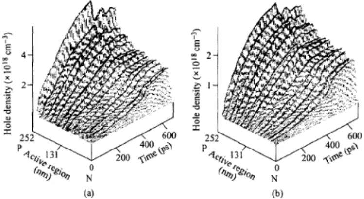
However, the charge neutrality requires that both electrons and holes have similar distribution in the multiple quantum wells. The theory expected that carriers did not distribute uniformly in the multiple quantum wells and their distribution favored the p-side. The calculated results are shown in Fig. 1 .8
Many studies had obtained the similar results. 13-15
Fig. 1 Calculation ofelectrons' and holes' distribution in the 14 layers ofquantum wells. It shows highly uneven-distribution properties. 8
The reason for carrier distribution favoring the QWs near the p-cladding is explained as follows. Because holes have much smaller mobility than electrons, they move much slower than electrons. When they are near the quantum-well region, a strong electric field is built between electrons and holes. The electric field then tends to pull electrons toward holes because of the high mobility of electrons. Therefore, electrons are forced to move from the n-cladding to the QWs near the p-cladding layer to satisfy charge neutrality. Moreover, because the electrons have longer capture time and shorter diffusion time, it is easier for electrons to reach the positions of holes. However, the above concept could not
explain our experiment that showed more carriers in QWs near n-side than near p-side. It will be described in the
following.
3. SEQUENCE INFLUENCE ON CARRIER DISTRIBUTION AMONG MQWS
The sequence of MQWs had been found to strongly influence the bandwidth of SOAs. 16 Mirror-imaged MQWs of
different types were used for the experiment. We used two MQW structures with the same MQWs, but opposite
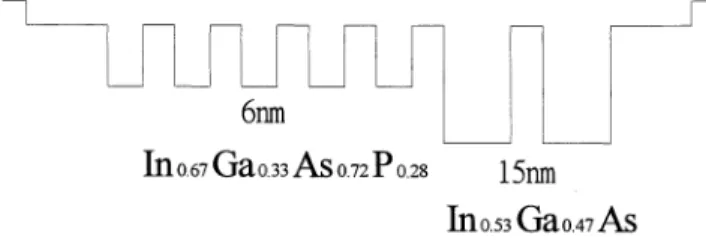
sequence of QW layout. The quantum-well structures have two In053Ga47As QWs and three In067Ga33As072P028 QWs.
The QWs are separated by wide In086Ga14As03P07 barriers. The In053Ga47As QWs are 8.7 nm wide, while the In067Ga33As072P028 QWs are 6 nm wide. The first sequence has the two In053Ga47As QWs near the n-cladding layer and the three In067Ga33As072P028 QWs near the p-cladding layer, as shown in Fig. 2. The second sequence has the
opposite layout, i.e., the two In053Ga47As QWs near the p-cladding layer and the three In067Ga33As072P028 QWs near
the n-cladding layer. The QW structure was grown using MOCVD. Bent-stripe ridge-waveguide SOAs were fabricated on those substrates. 17 The device length is about 5OOtm. Typical processing techniques were used for the device fabrication. The ridge waveguide was created by ME. No facet coatings were applied to the devices.
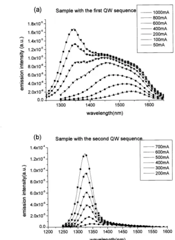
Figs. 3 (a) and (b) show the measured emission spectra ofthe three samples for different injection-current levels. Very distinct features ofthe emission spectra from the two samples of opposite QW sequence are clearly shown in Figs. 3(a) and (b). For the sample of the first QW sequence shown in Fig. 2, the emission at the low injection current occurs at the wavelength corresponding to the n=1 transition in the 8.7 nm In053Ga47As QWs. As the injection current slightly increases, the emission spectrum is then contributed from the simultaneous transitions of n1 and n2 states in the same QWs. The emission due to the 6 nm 1n067Ga033As072P028 QWs is not obvious until the injection current increased to above 400 mA. For the sample of the second QW sequence, the emission at the low injection current occurs at the
wavelength corresponding to the n=1 transition in the 6nm In067Ga033As072P028 QWs. Further increase of the injection
current does not obviously change the emission wavelength. The slight blue-shift of the peak wavelength is a result of
the band-filling effect in the 1n067Ga033As072P028 QWs. As we compare the emission spectra from the two samples, it is
clear that the first QW sequence has much broader spectral width than the second QW sequence.
In0 53Ga0 47As
Barrier: 1 5nm, Illo 86Ga0 14As0 3P0 SCH region: l2Onm, In0 86Ga0 14As0 3P07
Fig. 2 Schematic of QW structure nonidentical MQWs for the study of QW sequence influence on SOA bandwidth. U) C U) C C 0 U) U) E a) Ca U) C a) C C 0 U) U) E a)
Fig. 3 The emission spectra at different injection currents: (a) the first QW sequence shown in Fig. 1; (b) the second QW sequence opposite to the first QW sequence.
For the first QW sequence, the 8.7 nm In0 53Ga047As QWs are near the n-cladding layer. For the second QW sequence, the 6 nm 1n067Ga033As072P028 QWs are near the n-cladding layer. The measured spectra from the above samples show that the wells near the n-cladding layer accumulate more carriers than those near the p-cladding layer,
P In067Ga033As072P028
8.7nm
N
wavelength(nm) 1300 1350 1400 1450 1500 1550 1600 wavelength(nm)which is different from past observations. , In the past, the slow mobility of holes is deemed to be the reason for the nonuniform carrier distribution and leads to the carriers favoring QWs near the p-cladding layer. However, our new discovery shows that other factors could be influential as well and may be more important than the slow movement of holes. Therefore, we obtained the behaviors opposite to the past observation.
4. INFLUENTIAL FACTORS ON CARRIER DISTRIBUTION AMONG MQWS
Many factors have been studied to show their influences on the carrier distribution. Here we would like to address a new point of view. We assert that the type of carriers first arriving at the QWs will determine the carrier distribution. The reason is as follows. In the carrier injection, electrons and holes move from the n-cladding layer and the p-cladding layer, respectively. If electrons arrive at the QWs much earlier than holes, they will be captured in QWs nearest to n-cladding. At this time, holes are still far away from QW region, so electrons and holes are far apart. This leads to two effects. First, the band tilt across the separate confinement hetero-structure (SCH) layer and the QW region is small. Second, the electric field between the electrons and the holes is still small, so electrons are not significantly influenced by holes. As time goes on, holes continue to move toward QWs. When holes are close to QWs, the distance between the hole cluster and the electron cluster is very short. Thus theband tilt is large. It means that the electric field is strong and
holes tend to be pulled toward electrons instead of being captured into QWs near the p-cladding. This mechanism
causes holes to follow the electron distribution to achieve the condition of quasi-charge neutrality. Therefore, carrier distribution favors QWs near the n-cladding layer. On the other hand, if holes arrive at the QWs first, carrier distribution favors Qws near the p-cladding layer.
The overall effect depends on the summation of the diffusion time across the SCH layer and the capture time.
The diffusion time is given by d2 I4D,whered is the thickness of SCH layer and D is the diffusion constant. The capture time for electrons and holes is about 1 ps (r) and 0.2 ps (r,), respectively. 18,19 Becauseour layer structures
have a very thick SCH layer, the hole diffusion time is about 1 1 ps, which is much longer than the sum of the electron
diffusion time and the electron capture time. Thus electrons reside in the QWs before holes, leading to carrier
distribution favoring QWs near the n-cladding layer.
The influence of SCH layer thickness on the carrier distribution has also been experimented. We designed
samples with the same nonidentical MQWs, but the QW structures have different SCH layer thickness. SOAs/SLDs
were fabricated on the substrates with those QW structures. The measurements of emission spectra show that the
thinner SCH layer has broader emission spectra. This further confirms that the transport time of carriers across the SCH
layer has very strong influence on the carrier distribution. Our discovery suggests that carrier distribution can be
engineered to favor carriers in QW near the n-cladding layer, the p-cladding layer, or equally among QWs.
5. MQW STRUCTURE FOR BROADBAND EMISSION SPECTRA
With the above knowledge, we are able to design MQW structure that exhibits extremely broadband characteristics. The
layer structure is shown in Fig. 4. Compared to the previous structure, the two In053Ga47As quantum wells are designed to be 1 50 A, so the emission could extend to wavelength longer than 1 .55 tm. They are grown near the n-cladding layer. For short-wavelength side, we used five 60A In067Ga033As072P028 quantum wells in order to
compensate the possible absorption by the two In053Ga47As quantum wells. They are grown near the p-cladding layer. 1n086Ga014As03P07 barriers of 150A width are used to separate those QWs. The sequence of QW layout is the same as
the previous design 16forbetter uniformity of carrier distribution among MQWs.
1110.67 Gao.33 AS 0.72
P
0.2815i
1110.53 GaO.47.A.sFig. 4 Quantum-well structure of designed MQWs for broadband emission.
and tilted-stripe SLDs 20hadbeen fabricated using typical processing techniques. With those structures, the Fabry-Perot
resonance could be minimized, so the emission spectrum can be directly realized. The ridge waveguide was created by ME and etching was stopped at —100nmabove the separate confinement hetero-structure (SCH) layer. The fabrication is completed by n-contact metallization and then the devices were cleaved apart. No facet coatings were applied to the devices.
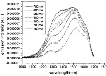
The emission spectra ofthe fabricated devices in different current levels were measured and shown in Fig. 5.Both
the bent-waveguide SLDs and the tilted-stripe SLDs behave similarly. The emission at the low injection current first occurs at the wavelength corresponding to the n=1 transition in the 150A 1n053Ga047As double QWs. However, the emission from the five 60A In067Ga33As072P028 QWs already appears even at the low injection current of 100 mA. As
injection current increases, emission contributed from the 60A In067Ga33As072P028 QW grows faster than that
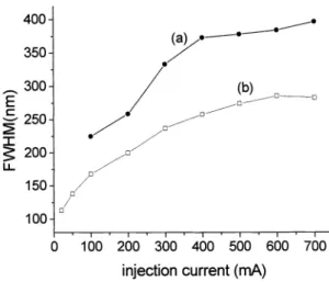
contributed from the In053Ga47As QWs, so the spectrum is very broad. The emission spectrum continues to broaden as the injection current increases. The spectral width is plotted against the injection current in Fig. 6. The FWHM of the
spectrum is already more than 200 nm for the injection current below 100 mA and increases fast for current up to 400mA. After this current level, the In053Ga47As QWs are filled with carriers. As a result, the emission from the In067Ga33As072P028 QWs is not absorbed by the In053Ga47As QWs. Further injection of carriers then stay in
In067Ga33As072P028 QWs, causing the corresponding emission of light to increase fast with the injection current. Therefore, the spectrum is very broad. The maximum FWHM spectral width is near 400 nm, covering from 1 252nm to
1643nm. 0.000011 0.000010 —: 0.000009 : 0.000008 ;: 0.000007
:
0.000006 C - 0.000005.
0.000004 C .2 0.000003 U) . 0.000002 0.000001 0.000000 -0.000001 1000 1100 1200 1300 1400 1500 1600 1700 1800Fig.5Theemission spectra at different injection current levels.
The FWHM ofthe emission spectrum from the previous MQW structure 16 also plotted in Fig. 6 for comparison. The previous MQW structure has gradual increase of spectral width. Its maximum spectral width is only around 300 nm at the injection current of 600 mA (curve (b) of Fig. 6). In comparison, Curve (a) in Fig. 6 shows that the spectral width has rapid increase for current below 400 mA. At current of -250 mA,the spectral width already reaches 300 nm. The maximum spectral width is about 400 nm, 30% more than the previous MQW structure. The fast increase of spectral
width at low injection indicates that the QW structure shown in Fig. 4 could have carriers reside in In067Ga33As072P028
QWs at low injection carriers. Thus the uniformity of carrier distribution is improved. The less measured emission at the
short-wavelength side is because its corresponding energy is large and the emission can be absorbed by the
In053Ga47As QWs.
If the number of In067Ga33As072P028 QWs is further increased, the broad spectrum should be achieved at even lower operation current. However, the sequence of QW layout still needs to be carefully considered, so carriers will
reside in the 150A In0 53Ga0 47As QWs, which contribute to the long-wavelength emission.
6. BROADLY TUNABLE SEMICONDUCTOR LASERS
In this section, we will report and discuss the possibility of using the above broadband SOAs as the gain media to
achieve the broadband tuning of semiconductor lasers.
400 350• -.' 300 E
-
250 200 U-I 50 I 00 0 '10 200
' 300 400 ' 500 600 700injection current (mA)
Fig.6 Spectra! width vs. injection current: (a) MQW structure shown in Fig. 4; (b) MQW structure shown in Fig. 1 16
6.1Influence of QW sequence on the tuning range
The influence of QW sequence on the carrier distribution among the MQW5 had been reported in Sec. 3 .Forthe well
sequence shown in Fig. 2, we can have carriers distributing among the two types of QWs, which have their n1
transition corresponding to wavelengths of 1 .3 im and 1 .55tim, respectively. The total gain spectrum can then cover
the range from below 1 .3 im to above 1 .55tim,depending on the injection current according to the calculation using
Luttinger-Koim method. 21,22 Incontrast, for the QW sequence opposite to the one shown in Fig. 2,carriersdistribute
mostly in the 6nm In067Ga33As072P028 QWs. Therefore, its gain spectrum covers the range mainly around 1 .3 .tm. The
SOAs with the two different QW sequences are used in the external-cavity configuration for tuning experiment. The cavity configuration is shown in Fig. 7. The bending side of the waveguide in the SOA faces the grating. Light emitted
from the facet is collimated and delivered to the grating. The output light is taken from the straight side of the
waveguide and collimated. Tuning is achieved by rotating the grating.
SOA
Fig. 7 Tunable semiconductor laser with an external-cavity configuration.
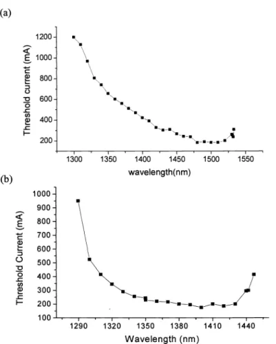
When the SOA with the QW sequence shown in Fig.2 is used in the cavity, the tuning range is very broad. Fig. 8(a) shows the threshold current vs. the tuning wavelength. The wavelength is tunable from 1300 nm to 1540nmwith a range of 240 nm. The experiment confirms that the SOA could provide gain for the same broad spectral range. On the other hand, if the SOA with the opposite QW sequence is used in the cavity, the tuning range is much narrower. It is now tunable from 1290 nm to 1450 nm with a range of 160 nm. The tuning range extends slightly further toward the
short wavelength side because carriers now more concentrate on the 6nm 1n067Ga033As072P028 QWs. However, tuning
toward the long wavelength side is severely limited due to the negligible carriers in the 1n053Ga047As QWs. This indicates that the SOAs with the opposite QW sequence only provide gain for the short wavelength.
Gratin
output
(a) 1200 E 1000 C 2 800 • D 600 0 _C 400 _C
•_.
F-2 00 100 1350 1400 1450 1500 • I 550 (b) wavelength(nm) 1000I !\
I 2 \NN.
}— 200 I 00 1290 1320 1350 1380 1410 1440 Wavelength(nm)Fig.8 Threshold current vs. tuning wavelength for using SOA with (a) QW sequence shown in Fig. 2 and (b) QW
sequence opposite to Fig. 2.
6.2 Broadly tunable semiconductor lasers with reduced operation
Fig. 8(a) shows that very broadband tuning can be achieved using SOAs with properly designed nonidentical QW
structure. The tuning range is 240 nm. However, the operation current is quite large. The reason is due to the bending waveguide structure, which induces two effects. First, the bending waveguide has more loss than the usual straight waveguide. Second, the light field may not be properly guided in the waveguide, leading to extra loss for coupling to
the external cavity. 23Toconfirm the possible reduction of operation current, we use the Fabry-Perot laser diode (LD) in the external cavity for tuning experiment. Again, the external cavity has a grating for the control oftuning wavelength.
The Fabry-Perot LD has the same QW structure shown in Fig. 2. Ridge-waveguide LDs were fabricated on the
substrate. The ridge width is about 3 im and the device length is 300 pm. No AR-coating is applied, so the device
oscillates at the current of 120 mA. The lasing wavelength is about 1360 nm. The short wavelength indicates that the current level is already large enough to shift the gain peak from the n1 transition of the Inos3Gao.47As QWs to the n=2 transition. In addition, carriers probably also distribute in the In067Ga33As072P028 QWs, so the gain at the short wavelength is increased to above the loss. When the LD is set up in the external cavity, additional feedback of light is delivered to the LD, so the loss level is reduced. This will cause the lasing threshold to reduce. Furthermore, the gain peak changes with the injection current, so the threshold varies with the lasing wavelength. In this way, we are able to use the uncoated Fabry-Perot LD in the external cavity to achieve broadband tuning. The threshold current vs. the tuning wavelength is shown in Fig. 9. The wavelength is tunable from 1344 nm to 1561 nm. The threshold current is below 116 mA for the tuning range of 217 nm. The minimum threshold current is 28.5mA at the wavelength of 1530
I 20
1oo
8O
-
60\.
40\\.
/
___,_. U-20• c:: I • I • 1350 1400 1450 1500 1550 1600 wavelength(nm)Fig.9 Threshold current vs. tuning wavelength using the Fabry-Perot LD in the external cavity.
7. CONCLUSION
In conclusion, the physics of carrier distribution among the MQWs are studied in detail. We discovered that carriers can distribute more in the QWs near the n-cladding layer than near the p-cladding layer. The reason is because the carrier is
not determined solely by holes. Electrons can be dominant in the carrier distribution, too. The situation can be
controlled by the layer structure of MQWs. Thus carrier distribution is possibly engineered. With properly design of MQWs, we are able to achieve broadband emission using two properly designed 1 50A 1n053Ga 047As QWs and five
60A 1n067Ga 033As 072P 0.28QWs.A spectral width covering a range from 1 .25 jim to 1 .65 jimhas been achieved. The
spectral width could be near 400nm. When the SOAs with broadband characteristics are used in the external cavity, the semiconductor laser is broadly tunable. The tuning range is from 1300 nm to 1540 nm using bending-waveguide SOAs in the cavity. However, the operation current is high due to the loss induced by the bending waveguide. If a Fabry-Perot LD with the same QW structure is used in the external cavity, the operation current is greatly reduced to below 1 16 mA.
The tuning range is still over 200 nm. The minimum threshold current can be as low as 28.5 mA.
8. REFERENCES
1 . T.R. Chen, L. Eng., Y. H. Zhuang, and A. Yariv, "Quantum well superluminescent diode with very wide emission
spectrum," App!. Phys. Lett. vol. 56, pp. 1345-1346, 1990.
2. T. Semenov, V. R. Shidlovski, and S. A. Safin, "Wide spectrum single quantum well superluminescent diodes at 0.8tm with bent optical waveguide," E!ectron. Lett., vol. 29, pp. 854-857, 1993.
3 .Ching-FuhLin, Bor-Lin Lee, and Bor-Jian Lin, "Broad-band superluminescent diodes fabricated on a substrate with
asymmetric dual quantum wells," iEEE Photon. TechnoL Lett., vol. 8, pp. 1456-1458, 1996.
4. X. Zhu, D. Cassidy, M. Hamp, D. Thompson, B. Robinson, Q. Zhao, and M. Davies, "1.4-tm InGaAsP-InP strained multiple-quantum-well laser for broad-wavelength tenability," IEEE Photon. TechnoL Lett., vol. 9, pp. 1202-1204,
1997.
5. H. S. Gingrich, D. R. Chumney, S.-Z. Sun, S. D. Hersee, L. F. Lester, and S. R. Brueck, "Broadly tunable external cavity laser diodes with staggered thickness multiple quantum wells," IEEE Photon. Techno!. Lett. ,vol. 9, pp.
155-157, 1997.
6. Ching-Fuh Lin and Bor-Lin Lee, "Extremely broadband AlGaAs/GaAs superluminescent diodes," App!. Phys. Lett., vol. 71, pp. 1598-1600, 1997.
7. Bing-Ruey Wu, Ching-Fuh Lin, Lih-Wen Laih and Tien-Tsorng Shih, 'Extremely Broadband InGaAsP/InP
Superluminescent Diodes, "lEE Electron. Lett. 36, pp. 2093-2095, 2000.
8. N. Tessler and G. Eisenstein, "On carrier injection and gain dynamics in quantum well lasers", IEEE J. Quantum Electron., vol. 29, pp.1586-1595, 1993.
9. H. Yamazaki, A. Tomita, M. Yamaguchi, and Y. Sasaki, "Evidence of nonuniform carrier distribution in multiple quantum well lasers," Appi. Phys. Lett. 71, pp. 767-769, 1997.
1 0. J. Piprek, P. Abraham, and J. E. Bowers, "Carrier nonuniformity effects on the internal efficiency of
multipquantum-well lasers," App!. Phys. Lett. 74, pp. 489-491, 1999.
1 1 . B. L. Lee, C. F. Lin, J. W. Lai, and W. Lin, "Experimental evidence of nonuniform carrier distribution in
multiple-quantum-well laser diodes," Electron. Left., vol. 34, pp. 1230-123 1, 1998.
12. D. Tauber and J. E. Bowers, "Dynamics of wide bandwidth semiconductor lasers," from "High Speed Diode
Lasers," Editor: S. A. Gurevich, pp. 1-40, World Scientific, Singapore, 1998.
13. H. Hilimer and S. Marcinkeviius, "Optically detected carrier transport in 111/VsemiconductorQW structures: experiments, model calculations and applications in fast 1.55im laser devices", Appl. Phys. B, vol. 66, pp. 1-16,
1998.
14. J. Piprek, P. Abraham, and J. E. Bowers, "Carrier nonuniformity effects on the internal efficiency of
multiquantum-well lasers", Appl. Phys. Left., vol. 74, pp. 489-491, 1999.
15. T. C. Newell, M. W. Wright, H. Hou, and L. F. Lester, "Carrier distribution, spontaneous emission and gain
engineering in lasers with nonidentical quantum wells", IEEE J. of Selected Topics in Quantum Electron., vol. 5, pp. 620-626, 1999.
16. Ching-Fuh Lin, Bing-Ruey Wu, Lih-Wen Laih, and Tien-Tsorng Shih, "Sequence influence ofnonidentical InGaAsP quantum wells on broadband characteristics of semiconductor optical amplifiers/superluminescent diodes," Opt. Left.
26,pp. 1099-1101, 2001.
17.Ching-Fuh Lin and Chaur-Shiuann Juang, "Superluminescent diodes with bent waveguide", IEEE Photon. Technol.
Left.8, pp.206-208, 1996.
1 8. M. Alam and M. Lundstrom, "Simple analysis of carrier transport and buildup in separate confinement
heterostructure quantum well lasers," IEEE Photon. Technol. Left. 6, pp. 1418-1420, 1994.
19. S. C. Kan, D. Vassilovski, T. C. Wu, and K. Y. Lau, "On the effects ofcarrier diffusion and quantum capture in high speed modulation ofquantum well lasers," Appi. Phys. Left., 61, pp. 752-754, 1992.
20. G. A. Alphonse, D. B. Gilbert, M. G. Harvey, and M. Eftenberg: "High-power superluminescent diodes," IEEE J. Quantum Electron., 24, pp. 2454-2457, 1988.
21. D. Ahn and S. L. Chuang 'Optical gain and gain suppression of quantum well lasers with valence band mixing', IEEE J. of Quantum Electron., vol. 26, pp. 13-24, 1990.
22.S. L. Chuang 'Physics of Optoelectronic Devices', Chap. 9, John Wiley & Sons, New York, 1995.
23. Gagik Sh. Shmavonyan, Yi-Shin Su, and Ching-Fuh Lin, "Peculiarities of emission characteristics of semiconductor optical amplifier with multiple quantum wells, "Photonics West 2003, Paper 4986-52, San Jose, USA, 2003.