國 立 交 通 大 學
電子工程學系 電子研究所碩士班
碩 士 論 文
應用多層次結構製作之矽鍺奈米線於生物感測元
件上之靈敏度研究
The Study of the Sensitivity of SiGe Nanowire
Bio-sensor Device Fabricated with Multi-layer
(oxide/SiGe/Si-on-insulator) Structure
研 究 生:謝政廷
指導教授:張國明 教授
應用多層次結構製作之矽鍺奈米線於生物感測元件上
之靈敏度研究
學生:謝政廷 指導教授:張國明 教授 國立交通大學電子研究所碩士班 摘 要 在近幾年來的研究上,奈米線被廣泛的研究與探討,尤其是在生物 感測元件的應用上,被視為最具有潛力的元件之一。本實驗室的研究團 隊已成功的製作出矽鍺奈米線,並經由實驗量測後,證實矽鍺奈米線有 感測元件的特性。本論文中,我們利用半導體製程技術,製作出P型的 矽鍺奈米線,再使用電漿輔助型化學氣相沉積堆疊出氧化層,最後經由 氧化處理,使得矽鍺奈米線的鍺析出,成功的製作出非均質矽鍺奈米 線。我們使用不同濃度的矽鍺比例、不同氧化層的堆疊厚度以及不同的 氧化時間和不同的氮氣比例去做比較,最後找出具有最佳靈敏度的非均 質矽鍺奈米線。因此本論文所研究出的矽鍺奈米線,能有效的應用在生 物感測元件上。The study of the sensitivity of SiGe nanowire bio-sensor device fabricated with multi-layer (oxide/SiGe/Si-on-insulator) structure
Student : Cheng-Ting Hsieh Advisor : Dr. Kow-Ming Chang
Department of Electronics Engineering & Institute of Electronics National Chiao Tung University
ABSTRACT
Science on research in recent years, the nanowire was extensively studied and discussed, particularly in the application of bio-sensor devices, and is considered one of the most promising components for sensing devices. In our previous research, we successfully demonstrated the SiGe nanowire and by experimental measurement, we confirmed that is presented bio-sensor characteristic. In this thesis, p-type SiGe nanowires were fabricated, which is compatible to VLSI technology. Then we exploited plasma enhanced chemical vapor deposition (PECVD) to stack oxide layer. Next step, we oxidized SiGe nanowires to precipitate Ge, successfully fabricated non-homogeneous SiGe nonowires. We use the proportion of different concentrations of silicon germanium, stack of different thickness of oxide layer, different oxidation time and ratio of different nitrogen to compare. Finally, we found non-homogeneous SiGe nanowires, which had the best sensitivity. In ours results, SiGe nanowires presented the better application in bio-sensor device.
誌 謝 首先要感謝 張國明教授在這兩年中的指導,老師認真的教學精神 和開明的態度讓我不但在學術研究上學習到更謹慎的思考,也在日常生 活上獲益良多。更重要的是得以一窺半導體領域的深奧。 再來是要感謝實驗室的學長、同學、學弟們與指導和協助我完成論 文以及實驗的陳巨峰學長、劉重顯學長以及吳金濘同學,很感謝你們在 實驗上的指導、建議和協助,讓我在研究論文時可以學到很多專業知識 並且順利完成。另外也要特別感謝同屆的同學,並恭喜我們順利走過這 帶有汗水以及淚水交織的兩年。實驗室的致瑋、柏文學弟們當然也不能 忘記,你們的幫忙以及搞笑我銘感在心。 本論文的完成另外亦得感謝國家奈米元件實驗室(NDL)與交通大學 奈米中心(NCTU-NFC)的大力協助,因為有你們提供良好的實驗環境和 設備使我順利完成研究,並感謝所有的工程師、技術員和客服人員們。 最後,更感謝我的父母,謝春明先生與陳芬碧女士,感謝他們對我 從小到大的養育和栽培,在生活上給我無微不至的關心,在我情緒低落 時帶給我溫暖及鼓勵,讓我得以全心完成學業。我相信他們會以我為榮。
Contents
Abstract (Chinese)………..I Abstract (English)………..II Acknowledgement……….III Contents……… IV Figure Captions………VII Chapter 1 Introduction ... 11.1 Overview of nanowire sensors ... 1
1.2 Silicon nanowire fabrication ... 2
1.2.1 Bottom-up approaches of SiNW fabrication ... 2
1.2.2 Top-down approaches of SiNW fabrication ... 4
1.3 Applications of SiNW sensors ... 5
1.3.1 pH sensor ... 6
1.3.2 DNA sensor ... 7
1.3.3 Gas detection ... 7
1.3.4 Protein detection ... 8
1.3.5 Virus detection ... 8
1.4 Other materials of nanowire sensors ... 9
1.4.1 Metal oxide nanowire sensor ... 9
1.4.2 Conducting polymer nanowire sensor ...11
1.4.3 Metal nanowire sensor ...11
1.5 Sensitivity ... 12
1.6 Ge condensation technology ... 13
1.7 The oxidation mechanism of SiGe ... 14
Chapter 2 Experiment ... 16
2.1 Process flow ... 16
2.2 Functionalization... 18
2.3 Measurement of electric characteristics ... 19
2.4 Define the sensitivity ... 19
Chapter 3 Results and Discussions ... 20
3.1 Motive of the experiment ... 20
3.2 Nanowires cross-section view ... 21
3.2.1 Nanowires cross-section view of SEM ... 21
3.2.2 Nanowires cross-section view of TEM ... 22
3.3 Electrical response after dripping APTMS and BS3... 22
3.4 The sensitivity of SiGe nanowire with different stacked structures and Ge concentrations ... 23
3.4.1 Comparing with sensitivity of different stacked structures ... 23
3.4.2 Comparing with sensitivity of different Ge concentrations ... 25
3.4.3 Comparing with sensitivity of different stacked structures and Ge concentrations ... 26
3.5 The sensitivity of SiGe nanowire after the different of oxygen/nitrogen ratio of oxidation ... 27
3.5.1 Comparing N2 0%, N2 13% and N2 100% at 3 minutes ... 27
3.5.2 The comparison between N2 0% and N2 13% at different minutes .. 29
3.5.3 The raise of sensitivity after the better oxygen/nitrogen ratio of oxidation 29 3.6 The sensitivity of SiGe nanowire with different oxidation time ... 30
3.6.1 Comparing different oxidation time without PECVD oxide ... 30
3.6.2 Comparing different oxidation time with/without PECVD oxide .... 31
3.6.3 The raise of sensitivity after better oxidation time and structure ... 32
Chapter 4 ... 34
Chapter 5
Future Works ... 36 Reference………..81
Figure Captions
Chapter 1
Fig. 1-1 Numerical simulation result of the relationship between the response time (ts) and the detectable concentration (ρ0) of a DNA sensor ... 37
Fig. 1-2 Nanowire growth process ... 37 Fig. 1-3 The SEM images of SiNWs ... 38 Fig. 1-4 (a) Schematic illustration of vapor-liquid-solid nanowire gowth mechanism including three stages. (b) To show the compositional and phase evolution during the nanowire growth process. ... 38 Fig. 1-5 The process of nanoimprint lithography ... 39 Fig. 1-6 Schematic view of the NW transfer steps by trilayer NIL on The imprinted SU8/SiO2 IPMMA structure ... 39
Fig. 1-7 (a)–(d) Key fabrication flow, (f) top view of the device structure, and(e) cross-sectional view along the dashed line A to B in (f) ... 40 Fig. 1-8 (A) Schematic illusrating the conversion of a NWFET into N W nanosensors for pH sensing. (B) Real-time detection of the conductance for an APTES modified SiNW for pHs from 2 to 9 (C) Plot of th e conductance versus pH (D) The conductance of unmodified SiNW (red ) versus pH. The dashed green curve is a plot of the surface charge density for silica as a function of pH ... 40 Fig. 1-9 Schematic representation of the fabrication process of SiNW arrays with fluidic channels ... 41 Fig. 1-10 Schematic representation of the principle of the SiNW array biosensor for DNA ... 41 Fig. 1-11 Tilted view image of Pd nanowires on Si substrate ... 42 Fig. 1-12 Schematic diagram of Pd nanowire hrdrogen sensor fabricated ... 42 Fig. 1-13 Nanowire-based detection of single viruses. (Left) Schematic shows two nanowire devices specific binding of a single virus to the receptors o n nanowire 2 produces a conductance change (Right) characteristic of th e surface charge of the virus only in nanowire 2 ... 43
Fig. 1-14 Selective detection of single viruses. Conductance (Upper) and optica l (Lower) data recorded simultaneously vs. time for a single silico n nanowire device after introduction of influenza A solution ... 43 Fig. 1-15 (A) I-Vd curves of In2O3 nanowire sensors before and after exposure to 1%
NH3.(Inset) Energy band diagrams of heavily doped In2O3 and NH3
molecules. (B) I-Vd curves of In2O3 nanowire sensors before and after
exposure to 1% NH3. (Inset) Energy band diagrams of lightly doped In2O3
and NH3 molecules ... 44
Fig.1- 16 Electrical responses of an unmodified polymer nanowire (A) to 100 nM biotin-DNA (single stranded) and avidin-embedded polypyrrole (200 nm) nanowires to 1 nM (B) and 100 nM (C) biotin-DNA. The responses were recorded on two separate polypyrrole-avidin nanowires ... 44 Fig. 1-17 Two methods for preparing metal nanowires based on electrochemica l step-edge decoration. a) Electrodeposition of an electronically conductive metal oxide nanowires followed by reduction in hydrogen. b) Direc t electrodeposition of metal nanowires. ... 45 Fig. 1-18 Current response of a palladium nanowire-based H2 sensor under exposure
to hydrogen/nitrogen mixtures ... 45 Fig. 1-19 Simulated conductance values as a function of the surface potential for the 200-nm-wide and 50-nm-wide wires ... 46 Fig. 1-20 Ternary phase diagram for the Si-Ge-O system at 1000 K and1 bar, calculated based on the thermochemical data ... 46
Chapter 2
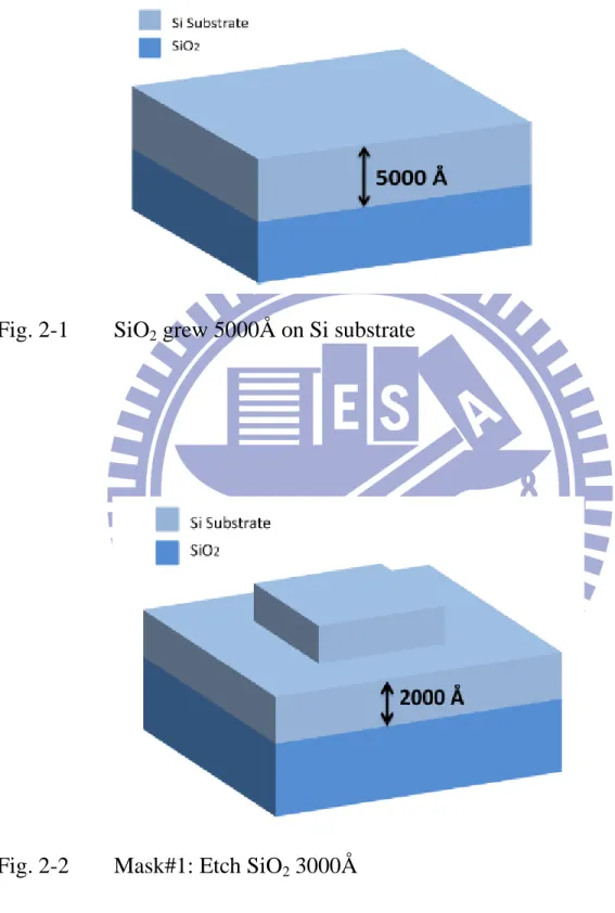
Fig. 2-1 SiO2 grew 5000Å on Si substrate... 47
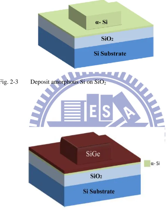
Fig. 2-2 Mask#1: Etch SiO2 3000Å ... 47
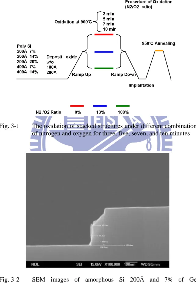
Fig. 2-3 Deposit amorphous Si on SiO2 ... 48
Fig. 2-4 Deposit amorphous SiGe on amorphous Si ... 48
Fig. 2-5 Mask#2: Define nanowire on the sidewall... 49
Fig. 2-6 Mask#3: Etch unwanted sidewall nanowire ... 49
Fig. 2-7 Deposit SiO2 by PECVD ... 50
Fig. 2-8 Implant Boron-fluoride (BF249+) into SiGe nanowires after oxidation and DHF treatment ... 50
Fig. 2-9 Deposit Al 5000Å on the devices... 51
Fig. 2-10 Mask#4: Define the Al contact position... 51
Fig. 2-11 The device view from top position ... 52
Chapter 3
Fig. 3-1 The oxidation of stacked structures under different combination o f
nitrogen and oxygen for three, five, seven, and ten minutes ... 53
Fig. 3-2 SEM images of amorphous Si 200Å and 7% of Ge concentration ... 53
Fig. 3-3 SEM images of amorphous Si 200Å and 14% of Ge concentration ... 54
Fig. 3-4 SEM images of amorphous Si 200Å and 20% of Ge concentration ... 54
Fig. 3-5 SEM images of amorphous Si 400Å and 7% of Ge concentration ... 55
Fig. 3-6 SEM images of amorphous Si 400Å and 14% of Ge concentration ... 55
Fig. 3-7 TEM images of amorphous Si 200Å and 7% of Ge concentration ... 56
Fig. 3-8 TEM images of amorphous Si 200Å and 14% of Ge concentration... 56
Fig. 3-9 TEM images of amorphous Si 200Å and 20% of Ge concentration... 57
Fig. 3-10 TEM images of amorphous Si 400Å and 7% of Ge concentration ... 57
Fig. 3-11 TEM images of amorphous Si 400Å and 14% of Ge concentration... 58
Fig. 3-12 The conductance of the PE oxide 100Å on 200Å 14% ... 58
Fig. 3-13 The sensitivity of the PE oxide 100Å on 200Å 14% ... 59
Fig. 3-14 The comparison current between amorphous 200Å and 400Å on N2 0% and PE oxide 100Å ... 59
Fig. 3-15 The comparison current between amorphous 200Å and 400Å on N2 0% and PE oxide 200Å ... 60
Fig. 3-16 The comparison sensitivity between amorphous 200Å and 400Å on N2 0% ... 60
Fig. 3-17 The comparison sensitivity between amorphous 200Å and 400Å on N2 13% ... 61
Fig. 3-18 The comparison current between PE oxide 100Å , 200Å and without P E oxide on 200Å 14% N20% ... 61
Fig. 3-19 The comparison sensitivity between PE oxide 100Å , 200Å and without PE oxide on 200Å 14% N20% ... 62
Fig. 3-20 I-V curve with different Ge concentration on PE oxide 100Å and α-Si 200Å ... 62
Fig. 3-21 I-V curve with different Ge concentration on PE oxide 200Å and α-Si
200Å ... 63
Fig. 3-22 I-V curve with different Ge concentration on PE oxide 100Å and α-Si 400Å ... 63
Fig. 3-23 I-V curve with different Ge concentration on PE oxide 200Å and α-Si 400Å ... 64
Fig. 3-24 Sensitivity with different Ge concentration on PE oxide 100Å and α-Si 200Å ... 64
Fig. 3-25 Sensitivity with different Ge concentration on PE oxide 200Å and α-Si 200Å ... 65
Fig. 3-26 The sensitivity with different concentration of Ge and different structures ... 65
Fig. 3-27 The sensitivity with different concentration of Ge and different ... 66
Fig. 3-28 The sensitivity with different concentration of Ge and different ... 66
Fig. 3-29 The percentage change of different structure on N2 0% ... 67
Fig. 3-30 The percentage change of different structure on N2 0% ... 67
Fig. 3-31 The sensitivity of different N2/O2 ratio on 200Å 7% ... 68
Fig. 3-32 The sensitivity of different N2/O2 ratio on 200Å 14% ... 68
Fig. 3-33 The sensitivity of different N2/O2 ratio on 200Å 20% ... 69
Fig. 3-34 The sensitivity of different ratio of nitrogen at 3 min ... 69
Fig. 3-35 The sensitivity of different ratio of nitrogen at 5 min ... 70
Fig. 3-36 The sensitivity of different ratio of nitrogen at 7 min ... 70
Fig. 3-37 The sensitivity of different ratio of nitrogen at 10 min ... 71
Fig. 3-38 The percentage change of different ratio of nitrogen on 200Å 7% at 3min ... 71
Fig. 3-39 The percentage change of different ratio of nitrogen on 200Å 14% at 3min ... 72
Fig. 3-40 The percentage change of different ratio of nitrogen on 200Å 20% at 3min ... 72
Fig. 3-41 The sensitivity on N2 13% and 200Å 7% under different minutes ... 73
Fig. 3-43 The sensitivity on N2 13% and 200Å 20% under different minutes ... 74
Fig. 3-44 The sensitivity on N2 13% and 400Å 7% under different minutes ... 74
Fig. 3-45 The sensitivity on N2 13% and 400Å 14% under different minutes ... 75
Fig. 3-46 The sensitivity with different thickness of oxide on N2 13% and 200Å 7%
under different minutes ... 75 Fig. 3-47 The sensitivity with different thickness of oxide on N2 13% and 200Å 14%
under different minutes ... 76 Fig. 3-48 The sensitivity with different thickness of oxide on N2 13% and 200Å 20%
under different minutes ... 76 Fig. 3-49 The sensitivity with different thickness of oxide on N2 13% and poly
silicon under different minutes ... 77 Fig. 3-50 The sensitivity with different thickness of oxide on N2 13% and 400Å 7%
under different minutes ... 77 Fig. 3-51 The sensitivity with different thickness of oxide on N2 13% and 400Å 7%
under different minutes ... 78 Fig. 3-52 The sensitivity with different PE oxide on N2 13% and 200Å 7% under
different oxidation time ... 78 Fig. 3-53 The sensitivity with different PE oxide on N2 13% and 200Å 14% under
different oxidation time ... 79 Fig. 3-54 The sensitivity with different PE oxide on N2 13% and 200Å 20% under
different oxidation time ... 79 Fig. 3-55 The variation of percentage on different Ge concentration under different oxidation time ... 80
Chapter 1
Introduction
1.1 Overview of nanowire sensors
In recent years, many of researches have been focused on the development of ultrasensitivity nanowire sensors. These sensors have a wide variety of potential applications [1]. Due to the large surface-to-volume ratio, silicon nanowire sensor provides a high sensitivity in the chemical or biological detection. In view of above unique feature, physical properties of nanowire were greatly influenced by surface adsorption of chemical species or biomolecules, such as electrical or optical signal.
For nanowire sensors operated as FETs, the sensing mechanism is the field-gating effect of charged molecules on the carrier conduction inside the nanowire. The advantages of nanowire FET sensor were lable-free, selective real-time detection, direct electrical readout and high density of device, which were also the advantage in nanowire bio-sensors. According to other researches, we found the nanowire-based sensors that exhibited faster response and the higher detection limit than other planar sensors, like chemical field-effect transistor (CHEMFET) and ion-sensitive field-effect
(ISFET). In Fig.1-1 [2], we clearly found out that the detection limit of nanowire-based sensors was three to four orders higher than planar sensors.
Semiconductor nanowires composed of silicon or other materials also can function as FET devices. There were lots of nanowire-based chemical sensors, including silicon nanowires, polymer nanowires, metal-oxide nanowires, metal nanowires and nanotubes. Silicon nanowires (SiNWs), one of the best characterized for bio-sensing applications [3].
Many of researches demonstrate that nanoscale device such as nanowires, carbon nanotubes, and nanoparticles are ultrasensitive sensors due to their one-dimensional (1D) structure. The 1D structure, such as nanowires, are particularly compelling due to their potential for biosensing applications and suitability for large-scale high-density integration [4].
1.2 Silicon nanowire fabrication
Silicon nanowire fabrication methods can be divided roughly into two groups: bottom-up and top-down methods.
1.2.1 Bottom-up approaches of SiNW fabrication
We briefly introduce here the bottom-up methods for nanostructure. The bottom-up method means that nanostructures are certainly formed on substrate under certain conditions. We know that a lot of nanowire synthesis methods are developed for bottom-up technology. And we introduce the following three methods for bottom-up formation which include laser
ablation, thermal evaporation and vapor-liquid-solid (VLS).
First, we introduce the method of laser ablation. Maroles, Lieber and their groups [5] used the Fe-Si target and the content of Fe in the target was 10%. The nanowire growth model of laser ablation was shown in Fig. 1-2. In this model, laser ablation of the Si1-xFex target produces a vapor of Si and Fe
that rapidly condenses into Si-rich liquid nanoclusters, and when the nanoclusters become supersaturated, the coexisting Si phase precipitates and crystallizes as nanowires. Ultimately, the growth terminates when the gas flow carries the nanowires out of the hot zone of the furnace.
Second, we introduce the method of thermal evaporation. Pan and co-workers successfully used thermal evaporation to make SiNWs [6]. Si substrate was oxidized in air at high temperature to produce a layer of silicon oxide on Si surfaces to study the effect of the oxide layer on the growth of SiNWs. To investigate the effects of pressure and temperature, the growth conditions were changed in a pressure range from 50 Pa to one bar and a temperature range from 800 to 1100 ℃ . The SEM images of SiNWs produced by thermal evaporation based on Si substrate in Fig. 1-3. It is noted that the method is convenient for the bulk quality growth of SiNWs.
Finally, we introduce the method of vapor-liquid-solid (VLS). Wu and co-workers successfully used vapor-liquid-solid (VLS) to make SiNWs [7] in following process, alloying, nucleation and axial growth. They used Au for metal catalyst. When increasing amount of Ge vapor condensation and dissolution, Ge and Au form an alloy and liquefy. The volume of the alloy droplets increases, and the elemental contrast decreases while the alloy composition crosses sequentially. Thus, with the concentration of Ge saturated in Au, the Ge would precipitate to form Ge nanowire. The process and phase diagram were shown in Fig. 1-4 (a) and (b). Advantages accruing
from VLS crystal growth are many. For example, highly perfect crystals can be prepared at a lower temperature than is possible in direct deposition from vapor onto a solid.
1.2.2 Top-down approaches of SiNW fabrication
We briefly introduce here the top-down methods for nanostructure. Top-down methods start with patterns made on a large scale and reduce its lateral dimensions before forming nanostructures. It approaches include lithography and etching process. Most of the VLSI technology is using this method to process because it can be easily to control pattern.
Traditional lithography is using the mask for patterning. A beam of light passes through the mask and a lens, which focuses an image on photoresist placed on a surface of a silicon wafer. The resolution of the
photolithographic process determines the critical dimension.
Previous studies have mentioned the Top-down fabrication processes of the SiNWs sensor with electron beam lithography (EBL) [8, 9] technology was easier scaling down than traditional lithography. The EBL technology enabled scale patterning with critical dimension under 30nm, even 10nm was achieved but the disadvantage of EBL technology was very expensive and longer process time.
Due to the EBL has some disadvantage, so it maybe replace with nanoimprint lithography. The advantage of nanoimprint lithography was low cost, high throughput, high resolution, and different linewidths with the same template. Nanoimprint lithography has two basic steps [10] as shown in Fig. 1-5. First, imprinting use a mold to create a thickness contrast pattern in a resist and move the mold. Second, pattern transfer use anisotropic
etching (RIE) to remove residue resist in the compressed areas. Next, we discuss more advanced method of nanoimprint lithography which can make 75nm wide nanowires. Wan and co-workers [11] have successfully used nanoimprint technology to create the nanowires to detect gas. The Fig. 1-6 was the nanowires fabrication by nanoimprint technology.
In the other way, the nanowires formation by sidewall spacer is also actively developing. The conformal deposition and anisotropic dry etching on pre-patterned surface were the significant factor to form the side spacer nanowires. The height and width of spacer nanowires were dominated by the thickness of thin film deposition and anisotropic etching time. Generally, the technique of sidewall spacer was prospective, possible, versatile and flexible. Lin and co-workers [12] have successfully used this method to fabricate the poly-Si spacer to be the channel for thin film transistor. Their steps flow and structure diagrams were shown in Fig. 1-7. In the other research, Kim and co-workers [13] have successfully demonstrated silicon single-electron transistors with sidewall depletion gates. In above studies, showed excellent reproducibility and controllability of spacer formation technology. In this study, we successfully used advantage of sidewall spacer formation to fabricate SiGe nanowires.
1.3 Applications of SiNW sensors
Due to the Si nanowires have lot of advantages, such as real-time, highly sensitivity, label free and large surface to volume ratio, the application of Si nanowire sensors were developed widely in chemistry and
biological, even based diagnostic tools. In this section, we would introduce some nanowire sensors, which were located importance on general researches, such as pH sensors, DNA sensors, gas sensors, protein sensors, and virus detection.
1.3.1 pH sensor
The first nanowire field effect devices had used to detect analytes in solution occurred in 2001 with the sensing of pH by Leiber’s group [14]. The device structure and chemical response were shown in Fig. 1-8. The SiNW device was transformed into a pH sensor by modifying the silicon oxide surface with and without 3-aminopropyltriethoxysilane (APTES). We could obviously found out that the p-SiNWs devices modified by 3-aminopropyltriethoxysilane exhibited stepwise increases in conductance as the solution pH was increased stepwise from 2 to 9. However, unmodified SiNWs device showed nonlinear response at low pH (2-6) and the same linear response with modified at high pH (6-9). At low pH, the –NH2 group
was protonated to –NH3 +
, which dominated reaction and formed positive charge on the surface. In contrast, at high pH, the –SiOH group was deprotonated to –SiO-, which dominated reaction and formed negative charge on the surface. Without modified 3-aminopropyltriethoxysilane, so it didn’t have the –NH2 group was protonated to –NH3
+
. Applying the positive charge depletes carriers and reduces the conductance in the p-type nanowire. In the same way, applying the negative charge accumulates carriers and increase the conductance in the p-type nanowire. This comparison clearly demonstrated that the sening mechanism was successful.
1.3.2 DNA sensor
Gao and co-workers [15] fabricated silicon nanowire arrays for label-free detection of DNA by top-down approach. The nanowire arrays fabrication process shown as Fig. 1-9. The electrical DNA assay described there is ultrasensitive, rapid and label-free, and is able to monitor directly DNA hybridization process in situ and in real time. The high sensitivity of nanowire sensors are prospective because the diameters of these sensors are similar to the size of the DNA molecules being sensed and because important signal changes will be caused by the binding of a small number of DNA molecules on the surface of a single nanowire. The analysis of working principle of the SiNW array biosensor is shown as Fig. 1-10. Simply, they used to determine the amount of conductance change in the binding of DNA with or without on the nanowire surface.
1.3.3 Gas detection
Kim and co-workers [16] used the electro-deposited into anodized alumina template approach of Pd nanowire fabrication to process the nanowire sensor for hydrogen gas sensor. The hydrogen sensor has been widely studied for a long time due to safety reasons. In their study, the hydrogen sensor utilizing a bundle of Pd nanowires is fabricated, which is shown in Fig. 1-11. The bottom gate was on Ti layer and the apparatus of sensor was shown in Fig. 1-12. They used a metal needle as the top contact because there was no other ways to make the excellent contact on the top of the Pd nanowires and to guarantee the hydrogen gas of reaching the nanowire surface. When the hydrogen gas flow presence in apparatus, Pd
metal is subject to swell because the Pd hydride has a larger lattice constant than pure Pd metal. Their groups utilized the characteristic, different sizes of metal have different conductance by measurement. As soon as the hydrogen gas was flowed to the sensing chamber, the electrical resistance of the Pd nanowire sensor stated to decrease suddenly. Overall, the sensor of hydrogen gas would be applied in the feature.
1.3.4 Protein detection
Wang and co-workers [17] demonstrate the sensor of protein molecules by using silicon nanowires fabricated by top-down approach. The Ab1 tyrosine kinase was covalently linked to the p-type SiNWs, which was set as surface modification. The sensing mechanism is similar previous studies. The observed increases in conductance are consistent with the binding of negatively charged ATP to Abl of nanowire surface. On the other hand, when SiNW is n-type, the conductance decreases as the ATP link to Ab1. The simple diagram of nanowire with or without ATP was shown in Fig. 1-12. If used the characteristic, there will be greater help on medical or drug analysis in the feature.
1.3.5 Virus detection
Lieber and co-workers [18] report rapid, label free, direct and real-time electrical detection of single virus particles with high selectivity by using nanowire field effect transistors. The different antibody receptors were covalently linked to the p-type SiNWs, which were set as surface modification, the diagram was shown in Fig. 1-13. We could find out that
modification of different nanowires within the array with receptors specific for different viruses provided a means for simultaneous detection of multiple viruses. And the Fig. 1-14 showed the conductance (upper) and optical (lower) data that was recored simultaneously. Overall, single viral particle sensitive, and capability of selective multiplexed detection of their approach suggest that this work could lead to useful viral sensing devices. This could provide an indication of mutations in samples as required for robust medical and bioterrorism detection, even drug discovery.
1.4 Other materials of nanowire sensors
There are many researches used Si nanowire as sensor, but other materials step by step respected in nanowire sensors. Not only the silicon are used as the material of sensor, there are other kinds of materials have been used as a nanowire sensor, such as metal oxide semiconductor nanowire sensor, polymer nanowire sensor, and metal nanowire sensor.
1.4.1 Metal oxide nanowire sensor
Metal oxide nanowire sensor had been determinate good potential to be used as chemical sensors in many recent researches. Many groups successfully demonstrated metal oxide 1-D nanostructure, which used as chemical sensors, involving nanowire [19], nanoribbon [20], nanobelt [21] nanorod [22], nanotube [23], and nanoparticle [24]. There are many kinds of metal oxide have been used as oxide of nanowire structure, involving ZnO, SnO2, In2O3, Co3O4, Fe2O3, TiO2, MoO3, and V2O5. The above mentioned
materials, especially, ZnO2, SnO2, and In2O3 were most attention on recent
researches.
Liu and co-workers [25] successfully demonstrated a field effect chemical sensor, which was based on ZnO nanowire. Their sensor were used to detect NO2 and NH3. They likely controlled the gate potential to affect the
sensitivity, and we clearly found out that when we want to desorb gas molecules on the surface we could apply a large negative voltage to reach. In other studies, ZnO nanostructures were developed in nanotube, nanocube, nanorod, and nanowire. Common feature of these nanostructures is large surface-to-volume ratio.
Nguyen and co-workers [26] successfully fabricated metal oxide nanowire in vertical field-effect transistor by buttom-up process that the materials including In2O3. Likewise, Zhang and co-workers [27] fabricated
and tested an In2O3 nanowire sensor, which could detect CO. Especially, the
sensor could detect in various atmospheres comprised of mixtures of N2/O2/CO, which is advantage in their research. It also obviously explained the detection of a wide range of sensor with the metal oxide nanowire. In other research, Zhang and co-workers [28] also fabricated the In2O3
nanowires as chemical sensor. Here, they used In2O3 nanowire sensor to
detect NO2 and NH3 at room temperature. The mechanism of gas sensor had
been introduced in section 1.3.3. Their nanowire sensor showed sensitivities as high as 106 for diluted NO2 and 10
5
for diluted NH3 and the diagram was
shown in Fig. 1-15, which showed the energy band diagrams and I-VD
curves. The response time was 10 sec for 1% NH3 and 5 sec for 100ppm
NO2. Thus, In2O3 nanowire sensor of gas detection will maybe apply in the
1.4.2 Conducting polymer nanowire sensor
Ramanathan and co-workers [29] successfully fabricated conducting polymer nanowire sensor, which had revolutionized to provide label-free, real time, high sensitivity, and selective detection of a wide range of chemical and biological. In Fig. 1-16 showed that the electrical response of an unmodified nanowire. Briefly, they have already demonstrated that the conductivities of Ppy or polyaniline can be modulated by simply controlling the oxidation state of these polymers. In other studies, several methods of polymer nanowire fabrication were electrochemical dip-pen lithography [30], mechanical stretching [31], electro-spinning [32], and template-directed electrochemical synthesis [33]. Summary, conducting polymer nanowire (CPNW) was fabricated by electrochemical polymerization.
However, CPNW was used as chemical or biological detection has several advantages, but we could find out that CPNW may not be biocompatible and postsynthesis assembly remained a problem, because CPNW was mechanically weak and not very reliable.
1.4.3 Metal nanowire sensor
Many of studies had successfully fabricated metal nanowire that used as chemical or biological detection, and the metal nanowires smaller than 100nm in diameter. In research of Walter and co-workers [34], they fabricated the metal nanowire by electrodeposition. Their studies suggest that metal nanowires might form the basis for chemical sensors. The formation of the structure was electrochemical step-edge decoration (ESED), which can be implemented in two different ways to obtain metal nanowire
arrays. The details of two methods are shown schematically in Fig. 1-17. This electrochemical step-edge decoration (ESED) supplies a new and very general method for preparing metal nanowires that possess important attributes involving adjustability of the diameter, great dimensional uniformity, strength, and lengths of more than 500μm. Generally, metal oxides such as copper, nickel, gold, and palladium can be selectively electrodeposited at the step edges present on the basal plane of highly oriented pyrolytic graphite (HOPG). In their other study [35], they successfully used the metal nanowire as efficient chemical sensors. The detection of hydrogen gas was shown in Fig. 1-18. We could obviously found out the resistance was decrease when H2/N2 flow in the apparatus at
room temperature. Therefore, it is used as the sensor of hydrogen gas is no doubt.
1.5 Sensitivity
The sensitivity for nanowire sensor was defined to the ratio of conductance, which was the value of shift. The nanowire sensor reveals higher sensitivity than other traditional planar sensor chiefly because of two arguments. First, the surface-to-volume ratio of the nanowire sensor is larger than other planar sensors. Second, it has the contribution of surface charges from sidewall. The argument was demonstrated [36] in Fig. 1-19, which shown the simulated conductance values as function of the surface potential for the 200-nm-wide and 50-nm-wide Si wires that the 50-nm-wide nanowire was more sensitive to 200-nm-wide nanowire, due to the surface-to-volume ratio of 50-nm larger than 200-nm.
We considered semiconductor nanowiers, such as Si and SiGe nanowires. According to the discussion of the paper [37], we could simply define the expression of conductance, conductance variation, and sensitivity respectively as follows: NW D L d N q G 4 2 0 (1.1) NW L d G (1.2) D qdN G G S 4 (1.3)
,where d : diameter, length of nanowire : LNW, uniform doping density : ND,
and q : 1.6 × 10⁻¹⁹ C.
1.6 Ge condensation technology
The process of oxidation of SiGe was also called Ge condensation because only Si during oxidation process was oxidized, and Ge was declined from pure SiO2 layer that caused increasing Ge concentration under oxide
layer. This phenomenon was first published in 1980s [38] and acquired a lot of attention because of at that time the importance of silicon germanium and germanium for electronic and optoelectronic devices [39]. Traditionally, in order to acquire SiGe film, the Ge has high concentration and great quality, it was essential to gradually increase Ge concentration during deposition,
caused by very thick SiGe film which was not practical. Many of groups had actively researched and demonstrated that ultrathin SiGe film with very high Ge concentration and great quality was achievable by process of Ge condensation.
In our research group, we would depend on the Ge condensation technology to implement size reduction and achieved increase of the Ge concentration at interface, which was used as material of nanowire and was great sensitive.
1.7 The oxidation mechanism of SiGe
The SiGe alloys exhibited higher carrier mobility than Si and could be thermal oxidized at relatively low temperature, so it was one of the most important materials for semiconductor device fabrication. In research of SiGe alloys [39, 40], they had efficiently demonstrated the oxidation mechanism of SiGe, which were explained by the diffusion kinetics and combination of oxidation kinetics in the following expression:
Si + O2 → SiO2 (1.4)
With Gibbs free energy change of ΔG1= -732 KJ/mol O2.
Ge + O2 → GeO2 (1.5)
With Gibbs free energy change of ΔG2= -376 KJ/mol O2. Combining above
two equations, it would obtain the third equation:
GeO2 + Si → Ge + SiO2 (1.6)
With Gibbs free energy change of ΔG3= -356 KJ/mol O2. According to
oxidized simultaneously when we oxidized the SiGe. Incidentally, Si was more active than Ge that had been demonstrated in many of researches. Moreover, from the energy change of ΔG3, we could find out that any Ge
oxidized would terminally be reduced by Si, resulting in pure SiO2 and Ge
accumulated at interface. According to the Fig. 1-20, we clearly realized while the Si existed, no GeO2 was formed under equilibrium. In other
researches [41, 42], they mentioned that the oxide layer on top of SiGe layer was not very thick and then Ge enhanced the oxidation rate of Si by a factor about 2~3 in wet oxidation and 1.5~2 in dry oxidation. Due to their studies, we could obviously know Ge concentration was higher when oxidation rate was increase. This interesting phenomenon was explained by both single crystalline SiGe and polycrystalline SiGe in both wet surrounding and dry surrounding.
Brief summary of SiGe and Si oxidation was raised in the following. Si interstitials injection was a factor that not only reduced oxidation rate but also greatly alleviated with the presence of Ge. Additionally, the vacancy flux from oxide to SiGe bulk was notify, which mean more Si atoms diffuse to the interface through vacancy and reacted with oxygen atoms.
Chapter 2
Experiment
In this study, we utilized the top-down fabrication method to fabricate SiGe/Si stack nanowires. In plain terms, we demonstrated SiGe/Si nanowires, which were nanometer scale on the spacer, instead of e-beam lithography and other complex buttom-up fabrication.
2.1 Process flow
A p-type Si substrate (100) was used in this study. The resistivity of silicon substrate was about 1~10Ω-cm.
1. Standard RCA clean and wet oxidation to grow 5000Å thick bottom oxide by SVCS Furnace system. The structure is shown in Fig. 2-1.
2. Mask#1: Define active area. TEL CLEAN TRACK MK-8 and Canon
FPA-3000I 5+stepper lithography system were employed to transfer
pattern onto oxide layer. Then, dry etching 3000Å was carried out with
TEL5000R.I.E system to form oxide step. It is ready for sidewall spacer
formation. The structure is shown in Fig. 2-2.
Vertical furnace system. This α-Si layer deposited 200A、400A and
separately for the stack structure. Then, α-Si served as seed layer for SiGe film deposition. The structure is shown in Fig. 2-3.
4. Standard RCA clean, and then SiGe was deposited by ANELAVA SiGe
UHV-CME. The structure is shown in Fig. 2-4.
5. Mask#2: Define S/D region and form spacer sidewall. Dry etching was carried out with TCP9400 SE poly etcher to define S/D region on the active layer and the SiGe/Si nanowires were defined on the spacer. The structure is shown in Fig. 2-5.
6. Mask#3: Remove unwanted sidewall spacer. TCP 9400 SE poly etcher was employed to remove unwanted spacer, which would have resulted in short circuit between two nanowire devices if not removed. The structure is shown in Fig. 2-6.
7. 100Å and 200Å of silicon dioxide were deposited on the SiGe/Si nanowires by PECVD PD-220N respectively. The structure is shown in Fig. 2-7.
8. Using the furnace tube to do surface treatment and etch the oxide by DHF.
9. Boron-fluoride (BF249+) was implanted into SiGe nanowires by E500HP
implanter. The implantation dose is focused on 1×10¹⁵ ions/cm2 and
10. Annealing in Furnace at 950℃ for 30min to activate dopants.
11. 4000Å ~5000Å Aluminum deposited by AST Peva 600I. The structure is shown in Fig. 2-9.
12. Mask#4: Define aluminum contact pad. Al pads are formed by wet etching (HNO3:CH3COOH:H3PO4:H2O=2:9:50:10). The structure is
shown in Fig. 2-10.
13. Aluminim sintering at 400℃ in N2 ambient for 30 min.
14. The device view from top position. The structure is shown in Fig. 2-11.
2.2 Functionalization
First, we dripped the DI water on the surface of the nanowires, the native oxide was around nanowires that set as linker. Second, we used amino-propyl-trimethoxy-silane (APTMS) to modify the surface of nanowires, and then the APTMS to oxide surface resulted in a surface terminating in both –NH2 and –SiOH groups. The diagram of modification
was shown in Fig. 2-11. After dripped the APTMS, the surface of the terminal of nanowires was amine groups. In our experiment, amine group would be as positive charge. It was similar that nanowires had the positive gate bias, so the conductance of P-type nanowires would be decreased. Next step, we dripped the bis-sulfo-succinimidyl substrate (BS3) on the nanowires,
which was modified by APTMS. BS3 treatment resulted in negative charge, so the conductance of the P-type nanowires would be increased. In this study, we focused on sensitivity of different surface treatment and different stack structures.
2.3 Measurement of electric characteristics
The electric characteristics of nanowire sensors were measured by HP4156A in our study. We applied the drain voltage (VD) from -10V to 10V
and step was 100mV, and didn’t apply the back gate voltage (VG). The
measurement of electric characteristics was achieved at every stage of surface modification, and the data of average conductance was extracted from ID-VD characteristics.
2.4 Define the sensitivity
In the beginning, we measured the I-V curve of devices which had dripped the DI water to the surface of SiGe nanowires, and then we defined the current was I0. Next step, we similarly measured the I-V curve of devices,
which had dripped the APTMS to the surface of SiGe nanowires, and then we defined the current was I. In our study, we used the above information and defined the sensitivity was S=
0 0 I
I I
. Overall, we would focus on the sensitivity of different conditions in our study.
Chapter 3
Results and Discussions
3.1 Motive of the experiment
According to our group’s previous researches, we concerned about oxidation time, Ge concentration, annealing temperature, and different of thickness of amorphous Si. We used our group’s previous researches for our foundation, and then we applied new process on the device. The new process used Plasma Enhanced Chemical Vapor Deposition (PECVD) technique to stack thin oxide layer before entering furnace oxidation. This new approach was the main purpose of increasing sensitivity. When we stacked thin oxide layer of about a few hundreds angstrom before entering furnace, the thin oxide could reduce Ge oxidation after entering furnace. If we could obtain more pure germanium nanowires, the mobility could be higher and the current could be similar increasing. However, the sensitivity should be increased when we successfully fabricated the structure.
In our group’s previous researches, we focused on different of annealing temperature, Ge concentration, and thickness of amorphous Si. At the annealing temperature, we focused on 950℃ because Ge would diffuse over 1000℃ and would not have energy to repair defects under 900℃. Due to above two reasons, we would set the annealing temperature of 950℃ in
order to improve the sensitivity of SiGe/Si nanowires. On the structure, we used nanowires of Poly Si, Si0.93Ge0.07, Si0.86Ge0.14 and Si0.20Ge0.80 in
combination of amorphous Si 200Å , 400Å and 100Å , 200Å thin silicon dioxide layer that the thin oxide layer was by PECVD. We would exploit above structures to find out the best combination in our experiment. The experimental procedure was shown in Fig. 3-1.
The treatment of oxidation was N2 0%, N2 13% and N2 100% at 900℃
for 3min, 5min, 7min and 10min. And then we also discussed the characteristics of SiGe/Si stack structure that had the same conditions unless without deposited oxide layer by PECVD in this chapter. Combining these conditions, we would find out the best sensitivity, whether there nanowires after deposited oxide layer by PECVD.
3.2 Nanowires cross-section view
3.2.1 Nanowires cross-section view of SEM
We observed the cross-section view of different structure and concentration nanowire by Scanning Electron Microscopy (SEM). The structure of 200Å 7% imaged Fig. 3-2, which showed the width of nanowire was 72nm. The structure of 200Å 14% imaged Fig. 3-3, which showed the width of nanowire was 77nm. The structure of 200Å 20% imaged Fig. 3-4, which showed the width of nanowire was 65nm. The structure of 400Å 7% imaged Fig. 3-5, which showed the width of nanowire was 67nm. The structure of 400Å 14% imaged Fig. 3-6, which showed the width of nanowire was 73nm.
3.2.2 Nanowires cross-section view of TEM
We observed the cross-section view of different structure and concentration nanowire by Transmission Electron Microscopy (TEM). The structure of 200Å 7% imaged Fig. 3-7. The structure of 200Å 14% imaged Fig. 3-8. The structure of 200Å 20% imaged Fig. 3-9. The structure of 400Å 7% imaged Fig. 3-10. The structure of 400Å 14% imaged Fig. 3-11.
3.3 Electrical response after dripping APTMS and BS3
We fabricated the p-type nanowires, and then the APTMS and BS3’s bond structure contained positive and negative electricity respectively. Consequently, the conductance would decrease after drip APTMS on p-type SiGe nanowire. Similarly, the conductance would be increased when the BS3 bond with nanowires after the APTMS dripped. The following sections will have many of the figures to illustrate the response.
We would introduce the calculation of sensitivity and show the response of conductance and sensitivity figures in our thesis. First, we dripped the APTMS on SiGe nanowires, and then we defined the sensitivity
S1= 100 0 0 1 I I I
. Second, we dripped BS3 on the SiGe nanowires, which were
after dripped APTMS, and then we defined the sensitivity S2= 100
1 1 2 I I I (I0:
dripped water current, I1: dripped APTMS current, I2: dripped BS3 current).
The example of conductance change was shown in Fig. 3-12 and the conditions were fixed on amorphous 200Å , Si0.86Ge0.14, 100Å oxide by
conductance decreased after dripped APTMS and the conductance increased after dripped BS3. According to the conclusions, we could confirm the nanowire had the characteristic of bio-sensor. The example of sensitivity variation was shown in Fig. 3-13. The sensitivity of dripped water was 1.082%. The sensitivity of dripped APTMS was -3.254%. The sensitivity of dripped BS3 was 2.663%. By the above results, we could obviously obtain the conclusion that we want. The conclusion was that the APTMS was positive charge, which could accumulate the p-type nanowire on the surface. And the BS3 was negative charge, which could deplete the p-type nanowire on the surface.
Then there must be note that we would focus the sensitivity S1 in the
following sections. For simplicity, we added absolute value, so the new
definition was S1=S= 100 0 0 1 I I I (3.1).
3.4 The sensitivity of SiGe nanowire with different stacked structures and Ge concentrations
3.4.1 Comparing with sensitivity of different stacked structures
In this section, we discussed whether the different structures have different sensitivity and focused the oxidation time at three minutes. We used and focused the multi-layer structure, which was oxide, SiGe and Si-on-insulator. Moreover, we also compared the similar structure, which was SiGe and Si-on-insulator. This structure was made prior to the study of our team. The following discussion we would frequently use this structure to
compare with our multi-layer structure. The main difference between these two structures was that the top of oxide layer. The top of oxide layer was deposition by PECVD and the thick was 100Å and 200Å . This oxide layer could control the rate of oxidation that possibly made lots of Ge precipitations on the surface. The stacked structure of bottom part was different thick of amorphous Si, which was 200Å and 400Å . The purpose was the amorphous Si with high resist, so the current flowed into the path of SiGe. When the amorphous Si was thick, the current of SiGe nanowire was enhanced.
First, we discussed the current and sensitivity of amorphous Si thickness on whether it would affect. We compared the thickness of amorphous Si on 200Å and 400Å and the I-V curve was shown in Fig. 3-14. We obviously observed the current of amorphous Si 400Å higher than 200Å . We used above instructions to explain this result. The Fig. 3-15, proved once again that the current of amorphous Si 400Å higher than 200Å on other different condition.
We also compared the sensitivity of 200Å amorphous Si and 400Å on different oxide layer thickness by PECVD that was shown in Fig. 3-16. We clearly observed the sensitivity of amorphous Si 400Å higher than 200Å on different oxide thickness or without oxide by PECVD. The results were that we glad to find. A large current would increase sensitivity. The Fig. 3-17, proved once again that the sensitivity of amorphous Si 400Å higher than 200Å on other different condition.
Second, we discussed the current and sensitivity of the top of oxide layer thickness by PECVD on whether it would affect. We compared the thickness of 100Å , 200Å and without oxide layer, and then the I-V curve was shown in Fig. 3-18. From the figure, we clearly found the thickness of
200Å had the higher current than 100Å and without oxide. Similarly, the 200Å of sensitivity also had higher than 100Å and without oxide that was shown in Fig. 3-19. The purpose of deposited oxide layer before entering furnace would reduce the oxidation rate, upgrade the quality of Ge by condensation, and reduce surface defects. Furthermore, we could get more pure germanium on the surface of nanowire. In the following sections, we would compare these structures in other different conditions, for example, on different nitrogen/oxygen ratio and different oxidation time. Overall, if there are no special conditions, then the sensitivity of treatment of oxide would be better than without oxide layer by PECVD.
3.4.2 Comparing with sensitivity of different Ge concentrations
In this section, we focused on the different Ge concentrations. The Ge concentrations were divided into 7%, 14% and 20%. We fixed the thickness of amorphous Si on 200Å and oxidation time at three minutes. The result of I-V curve was shown in Fig. 3-20 and Fig. 3-21, which fixed on thickness of 100Å and 200Å oxide layer by PECVD respectively. On the other hand, we also fixed the thickness of amorphous Si on 400Å and oxidation time at three minutes. The result of I-V curve was shown in Fig. 3-22 and Fig. 3-23, which fixed on thickness of 100Å and 200Å oxide layer by PECVD respectively. In this conclusion, we clearly found that whatever thickness of amorphous Si or both of thickness of oxide, as long as Ge concentration on the rise along with increased current. We know that the germanium has higher mobility than silicon, so the high concentration of Ge could make current enhance. The results of sensitivity were shown in Fig. 3-24 and Fig. 3-25. Similarly, we also could find as long as Ge concentration on the rise
along with increased sensitivity.
3.4.3 Comparing with sensitivity of different stacked structures and Ge concentration.
In this section, we would combine the different structures and different concentration of Ge to comparison and analysis. The sensitivity with different concentration of Ge and different structures were shown in Fig. 3-26. From the Fig. 3-26, we could find several trends and would discuss. First, we obviously observed that sensitivity increased as the concentration of Ge increased. But without top of oxide layer had not this trend. The current should increase as the concentration of Ge increase. However, if Ge concentration is too high that will cause many defects, then the current would be decreased. So, we could find that before entering the furnace if the nanowires didn’t deposit oxide, the sensitivity would not increase when the Ge concentration increased. But when we deposited thin oxide layer before enter the furnace, the sensitivity of 20% Ge concentration was higher than 14%. In the conclusion, when we deposited thin oxide layer before oxidize, it would improve sensitivity of higher Ge concentration. It was by slower oxidation rate to improve the quality of germanium, the quality of oxide and reduce defects. The Fig. 3-27 and Fig. 3-28, proved once again that the sensitivity of amorphous Si 400Å higher than 200Å on identical concentration of Ge and the higher concentration of Ge had a good sensitivity. However, the higher concentration of Ge had a good sensitivity that must have been deposited thin oxide layer before oxidize under the premise. And then the sensitivity of amorphous Si 400Å was higher than 200Å on identical concentration of Ge that whether have been deposited thin
oxide layer before oxidize.
In order to more clearly express, we defined the raise percentage of sensitivity as the next equation.
The raise percentage of sensitivity (%) = 100%
i i f S S S (3.2)
Si was the sensitivity of no oxide layer by PECVD. Sf was the sensitivity
of 100Å or 200Å oxide layer by PECVD. The value showed the percentage change of sensitivity. The results were shown in Fig. 3-29 and Fig. 3-30. The 20% concentration of Ge had the higher upgraded, this result had been explained by above some description.
3.5 The sensitivity of SiGe nanowire after the different of oxygen/nitrogen ratio of oxidation
3.5.1 Comparing N2 0%, N2 13% and N2 100% at 3 minutes
In this section, we would compare 0% of nitrogen, 13% of nitrogen and 100% of nitrogen at three minutes. The purpose of oxidation was that the process with nitrogen could repair the vacancies of surface and improved the quality of oxide in order to increase sensitivity and oxygen could oxidize SiGe in order to obtain more pure Ge condensation on the surface of nanowire.
In previous research, our group added content of nitrogen of 13%, 40% and 66.6%, and we testified 13% of nitrogen could be best. So, in this thesis, we would focus on 13% of nitrogen. In other hand, we would also discuss 0% of nitrogen, which was pure oxygen and 100% of nitrogen, which was
pure nitrogen. From different previous experiments, we continue to add different structure to compare that was the top of oxide layer by deposition. Overall, we would compare different ratio of nitrogen and oxygen on different structures in the following.
First, we focused on amorphous Si of 200Å and Ge concentration of 7%. The result was shown in Fig. 3-31. In Fig. 3-31, we could obviously find that N213% had the best sensitivity in any structures, especially 200Å oxide layer
by PECVD. We obviously knew that the nitrogen could repair surface defects and oxidation could obtain more pure germanium of condensation. So, N2 13% had the best sensitivity, which was not surprise. And then N2
100% was pure nitrogen that only could repair surface defects but didn’t have oxidation. N2 0% was pure oxygen that only oxidation could obtain
more pure germanium of condensation but could not repair surface defects by nitrogen. By trade off, N2 0% had the higher sensitivity than N2 100%.
Under N2 0% condition, it could obtain more germanium on the surface
although didn’t repair by nitrogen. In other words, the condensation of germanium increased sensitivity, which was good efficiency. Perhaps, we should focus on how to obtain more pure germanium. We also could obviously observe the different top of oxide layer on N2 100% treatment, the
sensitivity almost had not variation. So, we only discussed N2 0% and N2
13% at five, seven and ten minutes oxidation time in following sections. Similarly, the Fig. 3-32 and Fig. 3-33, proved once again above conclusion. The sensitivity also had not variation on N2 100% treatment, and N2 13%
3.5.2 The comparison between N2 0% and N2 13% at different
minutes
In this section, we would compare 13% of nitrogen to 0% of nitrogen at different oxidation time. The result of three minutes was shown in Fig. 3-34, which was fixed on amorphous 200Å and 14% Ge concentration. In above section, we already knew the sensitivity of N2 13% was higher than N2 0% at
three minutes. Next, we would discuss other different oxidation time. The result of five minutes was shown in Fig. 3-35, which was fixed on amorphous 200Å and 14% Ge concentration. We once again obviously observed the sensitivity of N2 13% was higher than N2 0%. In order to more
clearly identify, we also compared 13% of nitrogen to 0% of nitrogen at seven and ten minutes. The result of seven minutes was shown in Fig. 3-36 and the result of ten minutes was shown in Fig. 3-37. No accident, the sensitivity of N2 13% was higher than N2 0%. In conclusions, we could
confirm when we flew in nitrogen in the oxidation process, the sensitivity would be better than pure oxygen in the oxidation process at any oxidation time we set. The most likely cause was through the nitrogen to repair interface defects.
3.5.3 The raise of sensitivity after the better oxygen/nitrogen ratio of oxidation
In this section, we would combine the different structures under different ratio of nitrogen. More clearly, we would focus on whether the top of oxide layer under different ratio of nitrogen, and then we exploited the raise percentage of sensitivity to illustrate.
First, we fixed on three minutes oxidation time. The result was shown in Fig. 3-38, which was on Si0.93Ge0.07 and 200Å amorphous Si. The definition
of raise percentage was the same of above sections.
The raise percentage of sensitivity (%) = 100%
i i f S S S (3.3)
From the Fig. 3-38, we obviously observed N2 13% had the higher raise
than other ratio of nitrogen. Especially, the thickness of 200Å by deposition had the highest raise. Simply, the reason of the highest raise percentage was not only nitrogen could repair defects but also the top of oxide layer could reduce oxidation rate that could obtain good oxide interface and the accumulation of Ge atoms at the interface. Identically, N2 100% almost no
change in percentage variation, the reason was explained in front section. The Fig. 3-39 and Fig. 3-40 had also similarly trend, which were on Si0.86Ge0.14 and 200Å amorphous Si and Si0.80Ge0.20 and 200Å amorphous Si,
respectively.
3.6 The sensitivity of SiGe nanowire with different oxidation time
3.6.1 Comparing different oxidation time without PECVD oxide
In this section, we combined all structure and treatment to discuss the raise of sensitivity under different oxidation time. And then, we were temporarily not discussed with the structure of the top oxide layer by PECVD in this section. In other word, we would first discuss the previous studies of our team in the following.
because it was the best ratio of nitrogen in previous studies. The Fig. 3-41, Fig. 3-42 and Fig. 3-43 were fixed on 7%, 14% and 20% concentration of Ge and amorphous Si 200Å under different minutes. The Fig. 3-44 and Fig. 3-45 were fixed on 7% and 14% concentration of Ge and amorphous Si 400Å under different minutes. Particularly, the condition of no treatment was the first time in this thesis. It means that without any oxidation treatment. From above figures, we could obviously observe some trends. First, the condition of no treatment was the worst sensitivity in any structures. The reason was very easy to explain, because the condition of no treatment couldn’t repair interface defects and couldn’t increase concentration of Ge on surface by oxidation. Second, the sensitivity at three minutes was the best and then the sensitivity decreased with longer oxidation time in any structures. One of the reasons may be with the longer oxidation time induced that the Ge diffusion overcame the accumulation of Ge atoms at the interface. In other words, a large number of germanium accumulated on surface but more large number of germanium diffused from surface. That caused that the concentration of germanium was reduced on the surface.
3.6.2 Comparing different oxidation time with/without PECVD oxide
We had discussed without the top of oxide layer by PECVD. In this section, we would compare under the different oxidation time, whether or not the top of oxide layer thickness would affect the sensitivity. In previous conclusions, we already knew that N2 13% had the better sensitivity, so we
possibly focused on the condition of N2 13%.
First, we focused on amorphous Si 200Å and 13% of nitrogen. The Fig. 3-46, Fig. 3-47 and Fig. 3-48 were fixed on 7%, 14% and 20% concentration
of Ge under different minutes. From these figures, we could observe some trends. The longer the oxidation time would lead to lower sensitivity in the absence of the top of oxide layer by deposition. If it exist top of oxide layer before oxidation, the sensitivity would not lower with longer oxidation time. The best sensitivity was in the oxidation time of five minutes. In the previous discussion, we knew that when the oxidation time was long, the large of Ge by condensation would be diffusion to buried oxide, and then the surface of nanowire would not have higher Ge concentration. The fabrication of top of oxide layer would reduce oxidation rate and increase concentration of Ge on the nanowire surface. For the condition of reduce oxidation rate, we already had example of success. The Fig. 3-49 showed the poly silicon nanowire with or without top of oxide layer under different oxidation time. The best sensitivity was at ten minutes and without oxide, because its oxidation rate was faster to lead more thin nanowire, so sensitivity was better than other. Similarly, 200Å of the oxide layer had the worst sensitivity because the oxide layer suppressed oxidation rate to lead the nanowire couldn’t thinner. The top of oxide layer although could suppress oxidation rate but under longer oxidation time, the sensitivity would eventually reduce. So, 200Å of the oxide layer by deposition had the best sensitivity at five minutes in our experiment. The Fig. 3-50 and Fig. 3-51 were fixed on 7% and 14% concentration of Ge and amorphous Si 400Å under different minutes. Once again, they had the same conclusion.
3.6.3 The raise of sensitivity after better oxidation time and structure
According to the previous conclusions, we would find some good conditions to compare. We already knew that N2 13% better than other ratio,
so we possibly focused on the condition of N2 13%. From the Fig. 3-52, Fig.
3-53 and Fig. 3-54, we could obviously observe the best sensitivity under oxidation time of five minutes, also could clearly observe the better sensitivity on the condition of 200Å of the oxide layer by deposition. So, we would again focus on the condition of 200Å of the oxide layer by deposition. The variation of percentage was shown in Fig. 3-55. We already introduced the calculation of percentage in above sections, and then please refer the section of 3.4.3. The sensitivity of 20% concentration of Ge at five minutes oxidation time raised 150%. And as previously described and discussion, the sensitivity of 20% concentration of Ge by 200Å oxide layer had better than others, especially at five minutes.
Chapter 4
Conclusions
We could summarize the following result according to the research from previous experiment:
1. APTMS generated bond with BS3 and had the electrical response.
2. We successfully fabricated the SiGe nanowire by multi-layer structures, which were oxide, SiGe and Si-on-insulator, respectively. Furthermore, we exploited our previous stacked structure, which were 200Å 7%, 200Å 14%, 200Å 20%, 400Å 7% and 400Å 14%, and then combined the top of oxide layer by PECVD. The thickness of oxide layer by deposition was 100Å and 200Å . Above of all, they had the electrical response after APTMS modification.
3. In the case of oxidation time for three minutes, we found the multi-layer structure, which were oxide layer of 200Å , Ge content of 20% and amorphous Si 200Å that had the better sensitivity.
4. In the oxidation process flew in different proportion of nitrogen, which was 0% of nitrogen, 13% of nitrogen and 100% of nitrogen at oxidation time of three minutes, and the fabrication of nanowire was multi-layer structure. The previous study of our group had the same result on different proportion of nitrogen. The 13% of nitrogen had the better
sensitivity in any multi-layer structure.
5. Under different oxidation time, we successfully found the better sensitivity at five minutes. The conclusions of under different oxidation time were not corresponding on our previous experiments. The main reason was that we deposited oxide before oxidation. The oxide layer could reduce oxidation rate to lead more Ge accumulation on surface and suppress Ge diffuse to buried oxide.
6. In all of conditions, the structure of 200Å oxide layer, Ge content of 20% and amorphous Si 200Å on oxidation of 13% of nitrogen at five minutes had the best sensitivity.
Chapter 5
Future Works
Even though the sensitivity increased in my research, but there should be more methods to enhance the sensitivity. In the future works, we can focus on thicker top of oxide layer by deposition and more Ge content. Combination of new conditions, it maybe raised the sensitivity. Furthermore, the top of oxide layer was by PECVD and the chamber flew into N2O and
SiH4. We have a reasonable doubt that N2 plasma maybe could repair defect.
Perhaps, we could exploit the machine of PECVD to do N2 plasma
![Fig. 1-1 Numerical simulation result of the relationship between the response time (ts) and the detectable concentration (ρ 0 ) of a DNA sensor [2]](https://thumb-ap.123doks.com/thumbv2/9libinfo/8461114.183179/50.918.143.782.120.880/numerical-simulation-result-relationship-response-detectable-concentration-sensor.webp)
![Fig. 1-9 Schematic representation of the fabrication process of SiNW arrays with fluidic channels [15]](https://thumb-ap.123doks.com/thumbv2/9libinfo/8461114.183179/54.918.140.781.129.959/schematic-representation-fabrication-process-sinw-arrays-fluidic-channels.webp)
![Fig. 1-11 Tilted view image of Pd nanowires on Si substrate [16]](https://thumb-ap.123doks.com/thumbv2/9libinfo/8461114.183179/55.918.186.742.116.908/fig-tilted-view-image-pd-nanowires-si-substrate.webp)


![Fig. 1-19 Simulated conductance values as a function of the surface potential for the 200-nm-wide and 50-nm-wide wires [36]](https://thumb-ap.123doks.com/thumbv2/9libinfo/8461114.183179/59.918.141.795.149.963/fig-simulated-conductance-values-function-surface-potential-wires.webp)