應用於多媒體串流處理之可重組式運算單元硬體加速矽智產設計
79
0
0
全文
(2) 應用於多媒體串流處理之可重組式 運算單元硬體加速矽智產設計. Design and Implementation of an ALU Cluster Intellectual Property as a Reconfigurable Hardware Accelerator for Media Streaming Architecture. 研 究 生:張 紹 宣 指導教授:闕 河 鳴. Student:Shao-Hsuan Chang 博士. Advisor:Herming Chiueh. 國立交通大學 電信工程學系碩士班 碩士論文. A Thesis Submitted to Department of Communication Engineering College of Electrical and Computer Engineering National Chiao Tung University in Partial Fulfillment of the Requirements for the Degree of Master of Science in Communication Engineering July 2006 Hsinchu, Taiwan. 中華民國九十五年七月.
(3) 應用於多媒體串流處理之可重組式 運算單元硬體加速矽智產設計 研究生:張紹宣. 指導教授:闕河鳴 博士. 國立交通大學 電信工程學系碩士班. 摘要. 現在的生活裡,有著越來越多的行動式系統像是行動電話、MP3 播放器、 PDA、以及攜帶式電子遊樂器,其功能與複雜度都較過去上升。因此,對於行動 式系統來說大量的多媒體運算能力是必須的,而若是使用傳統的硬體架構來執行 這些運算,會因為架構上沒有很好的對應到多媒體檔案的特性,沒辦法很有效率 的對多媒體檔案作存取,會使得運算效能低落,最糟糕的是無法達到及時的需 求。本論文,為參考史丹佛大學所提出的串流處理器架構,設計了對應多媒體特 性的運算單元以提供所需運算能力,除此之外,在考量到了未來使用上的便利 性,以及能快速與真實的多媒體應用接軌,將此運算單元加上設計的介面電路後 使之成為能與 AMBA 相容的矽智產,如此便能在 ARM 的平台上,利用其他現成的 矽智產或是週邊,真實的將此設計變成多媒體運算所需要的硬體加速器。本論文 以軟式矽智產完成,並且經過 ARM 系列的基板驗證過所設計的介面電路,確定了 所設計的介面電路是符合 AMBA 規定的電路。. I.
(4) Design and Implementation of an ALU Cluster Intellectual Property as a Reconfigurable Hardware Accelerator for Media Streaming Architecture. Student: Shao-Hsuan Chang. Advisor: Dr. Herming Chiueh. Department of Communication Engineering National Chiao Tung University Hsinchu, Taiwan. Abstract There are more and more portable systems such as mobiles, MP3 player, PDA, and other entertainment systems in today’s life. The functionality and complexity of them thus increase much higher than old-time ones. Therefore, having a great deal ability of multimedia operation is important for portable systems. However, it is tough to have enough amounts of multimedia operations from conventional hardware architecture. This results from the poor match between conventional architecture and features of media applications. It hence leads to inefficient memory access that induces performance degression. The worst case is unable to meet the real time requirement. According, this thesis designs an operational unit, ALU cluster, that is referenced from Stanford’s stream processor architecture and thus matches to media applications to provide necessary processing requirements for media applications. Besides, considering the issues of convenient usage in the future and rapid integration of real multimedia applications, we wrap ALU cluster as an AMBA-compatible IP by adding designed interface. Then, it is possible to exploit other existing IP and peripherals in the AMBA platform and truly treats our design as hardware accelerator for real multimedia applications. This thesis is finished with a synthesizable soft IP. The designed interface is verified by ARM-series baseboard. This ensures that the interface conforms to AMBA specification.. II.
(5) ACKNOWLEDGMENTS. This thesis would not have been possible without the support of many exceptional people. First and foremost, thanks go to my research advisor, Professor Herming Chiueh. He has always been an inspiration to me and everyone else on this project through his vision and leadership. He also provided irreplaceable guidance for me when I needed for a fascinating problem, good advice, constructive criticism, support, and flexibility. I would also like to thank all team members of the SoC LAB group, especially my classmates over the years: We-Li Su and Joseph Tsai. They not only put up with me all of those years, but also made my days as an enjoyable graduate student. Finally, I can not say enough about the support provided by my family. My parents have been my biggest supporters and for that I am forever grateful. My girlfriend has always providing timely encouragement and advice. To all of my friends and family members who have helped me in one way or another over the years, I would like to say thanks.. III.
(6) CONTENTS. 摘要. I. Abstract. II. Acknowledgement. III. List of Table. VI. List of Figure. VII. Chapter 1 Introduction 1.1 Issues of Media Applications 1.2 Proposed design: An ALU Cluster Intellectual Property (IP) 1.3 Organization Chapter 2 Background 2.1 Reconfigurable Architectures for Media Applications 2.1.1 Stream Processor Architecture 2.1.2 Stream Processing Model 2.1.3 Implementations of Stanford’s Stream Processor Architecture 2.2 Design Methodology in the SoC Era 2.3 Overview of AMBA 2.3.1 Overview of AMBA AHB 2.3.2 Bus Connection 2.3.3 Signals of AHB Interface 2.3.4 Address Decoding 2.3.5 Basic Transfer 2.3.6 Transfer Type 2.3.7 Burst Operation 2.4 Overview of Emulation Environment 2.5 Summary. IV. 1 1 3 5 6 6 7 8 9 11 13 15 16 17 18 19 20 21 23 25.
(7) Chapter 3 Design and Implementation of an ALU Cluster Intellectual Property 3.1 An ALU Cluster 3.1.1 Architecture of an ALU cluster 3.1.2 Implementation Results 3.1.3 Chip Testing 3.1.3.1 Testing Environment 3.1.3.2 Testing flow and result 3.2 Design and Emulation for the AHB Slave Wrapper of Intellectual Property 3.2.1 Architecture of AHB Slave Wrapper 3.2.1.1 Finite State Machine of AHB Slave Wrapper 3.2.2 Modifications for Baseboard and Data Preparing 3.2.3 Emulation Result. 26 27 27 28 31 32 33 35. 3.3 An ALU Cluster Intellectual Property 3.3.1 Architecture of an ALU Cluster Intellectual Property 3.3.2 Functional Verification 3.3.2.1 Testbench: 16-tap FIR filter System 3.3.2.2 Simulation Results 3.3.3 Improvements from ALU Cluster to ALU Cluster IP 3.3.4 Extension of ALU cluster IP at magnetic RAM (MRAM) 3.3.4.1 Overview of MRAM 3.3.4.2 Modifications for MRAN 3.3.4.3 Implementation Result 3.4 Implementation Comparisons 3.5 Summary. 35 36 38 40 42 42 43 44 45 49 51 51 51 52 54 56. Chapter 4 Conclusion and Future Work. 57. Bibliography. 59. Appendix A: Assembly Code for Chip Testing A.1: Assembly Code for FIR A.2: Access Method for Memory Testing. 62 63 66. Appendix B: Memory Map. 69. V.
(8) LIST OF TABLES Table 2.1. SPECIFICATION OF STREAM PROCESSOR ARCHITECTURE. 10. Table 2.2. BURST SIGNAL ENCODING. 22. Table 2.3. ACTICE BYTE LANES FOR A 32-BIT LITTLE ENDIAN DATA BUS. 23. Table 2.4. ACTICE BYTE LANES FOR A 32-BIT BIG ENDIAN DATA BUS. 23. Table 3.1. SUMMARY OF AN ALU CLUSTER. 29. Table 3.2. TESTING RESULTS. 34. Table 3.3. MODIFICATIONS FROM ALU CLUSTER TO ALU CLUSTER IP. 49. Table 3.4. SUMMARY OF IMPLEMENTATION RESULTS. 53. Table 3.5. TABLE OF IMPLEMENTATED COMPARSIONS. 55. Table A.1. THE OPERATIONS CORRESPONG TO THE ALU UNIT. 62. Table A.2. THE OPERATIONS CORRESPONG TO THE MUL UNIT. 62. Table A.3. THE OPERATIONS CORRESPONG TO THE DIV UNIT. 62. Table A.4. ASSEMBLE CODE FOR FIR. 63, 64, 65. Table A.5. ACCESS TABLE FOR ODD BANK MEMORY. 66, 67. Table A.6. ACCESS TABLE FOR EVEN BANK MEMORY. 67, 68. VI.
(9) LIST OF FIGURES FIGURE 1.1.1. PROCESSOR-MEMORY GAP. FIGURE 1.2.1. PROPOSED ALU CLUSTER IP. FIGURE 2.1.1. STREAM PROCESSOR ARCHITECTURE. FIGURE 2.1.2. STREAM PROCESSING MODEL OF FIR FILTER SYSTEM. FIGURE 2.1.3. CHIP IMPLEMENTATION OF STREAM PROCESSOR. 2 4 8 9 10. ARCHITECTURE FIGURE 2.2.1. AN ASIC DESIGN. FIGURE 2.2.2. AN EXAMPLE OF PLATFORM DESIGN. FIGURE 2.3.1. A TYPICAL AMBA SYSTEM. FIGURE 2.3.2. DIAGRAM OF BUS CONNECTION. FIGURE 2.3.3. DIAGRAM OF AHB SLAVE. FIGURE 2.3.4. SIGNALS TO SELECT WHICH SLAVE. FIGURE 2.3.5. SIMPLE TRANSFER. FIGURE 2.3.6. TRANSFER WITH TWO WAIT. FIGURE 2.3.7. TWO KINDS OF BURST OPERATION. FIGURE 2.4.1. VERSATILE PLATFORM BASEBOARD FOR ARM926EJ-S. FIGURE 2.4.2. ARCHITECTURE OF VERSATILE PLATFORM BASEBOARD. FIGURE 3.1.1. ARCHITECTURE OF AN ALU CLUSTER. FIGURE 3.1.2. LAYOUT OF AN ALU CLUSTER. FIGURE 3.1.3. FLOORPLAN AND PAD ASSIGNMENT OF AN ALU CLUSTER. FIGURE 3.1.4. DIE MICRO PHOTO OF AN ALU CLUSTER. FIGURE 3.1.5. PACKAGE OF AN ALU CLUSTER. FIGURE 3.1.6. AN ALU CLUSTER ON THE PCB BOARD. FIGURE 3.1.7. LOGIC ANALYZER SYSTEM WITH LCD MONITOR DISPLAY. FIGURE 3.1.8. TESTING FLOW OF CHIP LEVEL TESTING. FIGURE 3.2.1. ARCHITECTURE OF AHB SLAVE WRAPPER. FIGURE 3.2.2. FINITE STATE MACHINE. FIGURE 3.2.3. PORTS MODIFICATIONS. FIGURE 3.2.4. MODIFICATIONS WITH ADDED REGISTER FILES. FIGURE 3.2.5. SOFTWARE CODES FOR ADS. FIGURE 3.2.6. ADDRESS DEFINITION. VII. 11 13 15 16 17 18 19 20 22 24 25 27 29 30 30 31 32 33 34 35 36 39 40 42 42.
(10) FIGURE 3.2.7. EMULATION RESULTS. FIGURE 3.3.1. ARCHITECTURE OF AN ALU CLUSTER IP. FIGURE 3.3.2. COEFFICIENTS OF THE FIR FILTER SYSTEM AND ITS INPUT. 43 43 44. FUNCTION FIGURE 3.3.3. EXPECTED OUTPUT RESULTS OF THE FIR FILTER SYSTEM. FIGURE 3.3.4. FULL WAVEFORM VIEW OF SIMULATION. FIGURE 3.3.5. DETAILED WAVEFORM IN EXECUTION STAGE A. FIGURE 3.3.6. DETAILED WAVEFORM IN EXECUTION STAGE B. FIGURE 3.3.7. DETAILED WAVEFORM IN READING STAGE A. FIGURE 3.3.8. DETAILED WAVEFORM IN READING STAGE B. FIGURE 3.3.9. MODIFICATIONS FOR MRAM WITH ADDED LOAD_STORE UNIT. FIGURE 3.3.10. LAYOUT OF AN ALU CLUSTER IP EXTENDED AT MRAM. FIGURE 3.3.11. FLOORPLAN OF AN ALU CLUSTER IP EXTENDED AT MRAM. VIII. 45 46 47 47 48 48 52 53 54.
(11) Chapter 1 Introduction. CHAPTER. 1. Introduction With the technology improving, there are many media applications related to our life such as mobiles, MP3 player, PDA, and other portable entertainment system. It is hard to avoid the usage of these products because it is convenient to use them for watching movies, listening to music, and even playing video games at anywhere and anytime. The functionality of them keeps growing day by day. Thus, the processing requirements of media applications are more and more important right now. However, the conventional architecture with only single processor is hard to handle all jobs by itself. Therefore, another solution according to the features of media applications must be brought up to overcome the growing processing requirements.. 1.1 Issues of Media Applications It is known that media applications have three main characteristics: large available parallelism, little data reuse, and a high computation to memory access ratio [1] [2]. The first one, large available parallelism, is due to each streaming is independent to others. Thus, each streaming is possible to be operated solely at the same time. Little data reuse results from the streaming element reading from the memory only accesses memory once and do not revisit again, causing poor performance to the cache in the conventional architecture. Large amount of data operations result in high computation to memory access ratio is needed is the third characteristic. All these characteristics are poorly matched to conventional architectures and the performance will be extremely awful while media applications running on conventional ones. It must have another dedicate design to solve these issues by multiple operational units and efficient bandwidth hierarchy.. -1-.
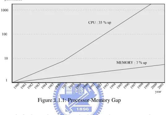
(12) Chapter 1 Introduction. From the media characteristics, we know memory access is the most serious problem for processing of media applications. In the mean time, the processor and memory performance gap that reveals the performance growing of memory is much slower than processor, as shown in Figure 1.1.1 [3]. This phenomenon will cause more latency for memory access. That means communication between processor and memory is more precious.. Figure 1.1.1: Processor-Memory Gap Fortunately, in the modern VLSI technology, as the process goes down to the deep submicron, it is possible to put lots of arithmetic logic unit (ALU) on a single chip in low cost [4] [5] [6]. It means that many operations are able to be executing at the same time by lots of functional units with little area cost. It is a great help for parallel processing. Summing up features of media applications and evolution of technology, there are many researches that are trying to improving the disability of conventional architecture by their own architectures such as Application Specific Integrated Circuit (ASIC), Platform-Based Architecture, and Reconfigurable Architecture. ASIC is specific to one application. It thus can have most balance to power, area, and performance. However, it lacks of flexibility to reuse design while the specification changes. Platform-Based Architecture consists of a processor core, memory, peripherals and other intellectual property (IP) with the same interface as hardware accelerator. By changing different IP, the same platform can be reused for distinct usages. The IP is mostly from ASIC by adding interface to solve different purposes. Although the flexibility of Platform-Based Architecture is better than ASIC, it still needs to change different IP for varied purposes. It is a characteristic, supporting application is limited, from ASIC. Therefore, Reconfigurable Architecture -2-.
(13) Chapter 1 Introduction. is another choice. It will use many general purpose operational units. As the demand is modified, the operational units are modified by reconfiguration, too. It therefore uses the same hardware to achieve different purposes. Details about architectures listed above and design methodology will be addressed in Chapter 2.. 1.2 Proposed design: An ALU cluster IP According to the issues of media applications and three associated architectures, we choose IP as a our target to process media applications, because we can get best trade-off from some physical issues, reuse other ready components to simplify developing efforts, and make our IP reusable for further possible development. In order to provide a more powerful ability for our IP, we reference from Stanford’s stream processor that is a reconfigurable architecture and thus develop our IP as a reconfigurable hardware accelerator for media applications [7]. The stream processor architecture is designed for media applications. Therefore, it matches the features of media ones and can handle them very well. However, it is a complete and huge system. Thus, it requires many human resources and much time to implement it. As a result, we select the processing part, ALU cluster, to be wrapped as an IP. Then, it can reduce efforts for developing a architecture to deal with media applications and be reused in the further. Details about stream processor architecture will be demonstrated in Chapter 2. The proposed design is shown in Figure 1.2.1. It is an ALU cluster IP that is compatible to AMBA-based platform. This platform may contain some available blocks such as processor, memory, other peripherals, and our intentional IP that is wrapped from an innovated ALU cluster from the stream processor architecture, as shown in the bottom part of the figure. Therefore, our proposed IP can be divided as hardware and software parts. The hardware part includes AMBA-AHB wrapper, ALU cluster, and memory. As for software, it must have architecture simulator to decide the number of internal operational units, depth of internal memory, and so on. The ALU cluster and architecture simulator are finished by our seniors last year [8] [9]. Taking these two previous designs as basement, some improvements are added to increase its performance that will be shown in Chapter 3.. -3-.
(14) Chapter 1 Introduction. Figure 1.2.1: Proposed ALU Cluster IP The advantages of the usage of the AMBA-based platform will be addressed in the Chapter 2. One major reason for choosing AMBA bus as a platform is because we take most care of connecting our design with real media applications. This can be benefited from the complete environment of AMBA bus. Except for the free specification of AMBA bus, there are already many baseboards and software that help to accelerate the design procedure. With these basebaords, there are mamy ready IPs, including processor core, memory, and peripherals, can be used directly. Besides, they are controlled by adequate software. Thererfore, these hardware and software are helpful to accelerate development. Details about the used platform and baseboard are in Chpater 2.. -4-.
(15) Chapter 1 Introduction. 1.3 Organization The motivation for the thesis is introduced in this Chapter. The remaining of organization about this thesis is as follow. In the Chapter 2, the first part will introduce architectures memtioned above for media applications, and the second part will discuss the design methodology. This section induces us to establish AMBA-base platform. Then, the overview of AMBA on-chip bus and AHB slave protocol will be presented. The last section is the introduction of emulation environment The Chapter 3 is the main chapter about the design and implementaion of the ALU cluster IP. The first section demonstrates the implementation results of ALU cluster, prototype I, and its testing outcomes. The second part is the hardware emulation of AHB wrapper by ARM baseboard. The following is the architecture, simulation results, and modifications of the ALU cluster IP. The last one is about IP that is extended to implement a real chip with magnetic RAM (MRAM) as data memory [10]. Then, the conclusion and future work will be addressed in the last chapter.. -5-.
(16) Chapter 2 Background. CHAPTER. 2. Background In this chapter, the related review of background about two architectures are used to deal with media applications, design methodology, AMBA specification of AHB protocol for the design, and used platform baseboard in this thesis is described. The first section will address reconfigurable architectures for media applications; they are DIVA and stream processor architecture [7] [11]. We will focus on stream processor architecture that is what we choose to further development. The second section is about the trend of design methodology, it reviews from ASIC to platform-based architecture. This section induces us to establish an AMBA-based platform that will advantage to further development. The third section is overview of the AMBA on-chip bus and the AHB slave protocol will be introduced most. As for the other details about AMBA bus, they could be found in the AMBA specification. The last section is about emulation environment that is our used platform baseboard in this thesis.. 2.1 Reconfigurable Architectures for Media Applications As we know from the introduction, media applications need an architecture that is different from conventional one to increase the processing requirements. Two kinds of architectures will be shown up. First, DIVA architecture will be introduced shortly. Then, the stream processor architecture is addressed. Brief speaking, DIVA is an architecture that integrates processor logic and memory in a processing-in-memory (PIM) chip. The advantages of its architecture is that internal PIM processors are directly connected to the memory banks, the memory bandwidth is dramatically increased (up to 2 orders of magnitude, tens or even hundreds of gigabits aggregate bandwidth on a chip). Latency to on-chip logic is also -6-.
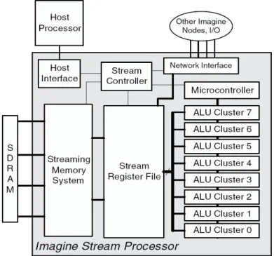
(17) Chapter 2 Background. reduced, down to as little as one-fourth that of a conventional memory system, because of the usages of internal memory access without the associated delays by communicating to off chip. It thus overcomes the large amount of memory demands and provides the ability to handle media applications. However, this architecture must have completely mechanism to communicate between each PIM. This will cause that extra efforts are needed to investigate the communications. Besides, the communicated protocol is not a general one that could not be portable to other hardware. Thus, it is not worthy to put much more efforts on it. We therefore choose stream processor as our reference architecture for further development. 2.1.1. Stream Processor Architecture. By trading off from features of media applications and growing technology, Stanford proposes the programmable stream processor architecture with three accents that are locality, concurrency and bandwidth hierarchy to better the processing performance of media applications. The stream processor architecture is shown in Figure 2.1.1 [12] [13]. It consists of ALU clusters, stream register file, streaming memory system, stream controller, micro controller, and host interface. The core of working part of that architecture is the eight ALU clusters. These eight ALU clusters achieve one of the features, the concurrency processing. They are controlled by microcontroller in single instruction multiple data (SIMD) manner. Therefore, all ALU clusters getting the same instructions from microcontroller and operate on different data streaming. Besides, these are very long instruction word (VLIW) instructions, performing compound stream operations on each streaming elements. There are many embedded local register files in the ALU clusters. The embedded local register files make the processing in local and accomplish the feature of locality. The streaming memory system is the interface to connect off chip SDRAM and is able to solve rare data bandwidth and provide ability to schedule dynamically. The stream register file is the novel organization of high performance memory pool and is used to store streaming of any length. Together with local register file, the stream register file can efficiently re-circulate streaming with different ALU clusters and perform the last characteristic of bandwidth hierarchy by storing the data from the streaming memory system to itself. By programming varied instructions, it is possible to execute different media applications. Stanford use stream processing model to map the media application into the stream architecture. The stream programming model allows simple control, makes explicit communication, and exposes the inherent parallelism of media applications. It will be discussed in next section. -7-.
(18) Chapter 2 Background. Figure 2.1.1: Stream Processor Architecture 2.1.2. Stream Processing Model. The processing flow of media applications is certainly like a sequence of computation kernels that operate on long data streaming. The kernel is a small program that repeats its operation for the continuous input streaming and produces the output streaming for the following subsequent kernels. The streaming is a variable length collection of records and these records are logical grouping of media data. An example of stream processing model is shown in Figure 2.1.2. It is one kind of media applications, the finite impulse response (FIR) filter system [14]. An FIR filter is a one dimensional convolution. It only has two kinds of kernel, MUL and ADD which are also the common operations in the media operations, over a long data streaming. Thus, the FIR filter system is a good demonstration for stream processing model. The equation 2.1 describes its operation: M −1. y[n] = ∑ bk * x[n − k ]. (2.1). k =0. The y[n] represents the output data streaming of the FIR filter system. It is the weighted average of the of input data streaming, x[n], from x[n] to x[n-M+1], with the weights given by the coefficients bk. The coefficient of n represents its instant time for both x[n] and y[n]. The coefficient of k stands for the number of taps in the filter, and bk is nth tap coefficient. -8-.
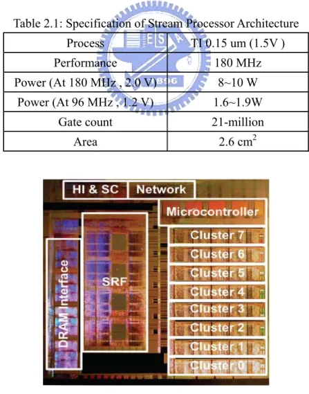
(19) Chapter 2 Background. Input Data. MUL. MUL. C0. C1. Filter Coefficients (C0 ~ Cn-1 ). MUL Cn-1. ADD. ADD. Output Data. Figure 2.1.2: Stream Processing Model of FIR Filter System The kernel in the stream processing model reveals the possibility to process media applications: parallel and pipeline execution. Multiple kernels can activate at the same time on independent streaming data. The front side kernel handles its input streaming and produces the output streaming and the streaming data is then passed to be processed by the next kernel. Therefore, the kernels are not only parallel but also pipeline to cope with the media data. Since all data are organized as streaming, only single memory access from off chip is required and the succeeding transfers are from register to register. It is helpful to optimize for bandwidth requirement. As a result, the memory bandwidth demands of the media applications can be solved by exploiting this stream processing model. Mapping the media applications to proper kernels and streams expose the characteristics that are enumerated in previous section, large available parallelism, little data reuse, and high computation to memory access ratio, so that the hardware can easily exploit them and achieve the needed performance requirements. 2.1.3. Implementations of Stanford’s Stream Processor Architecture We now take a look at Stanford’s work. The chip is shown in Figure 2.1.3. The. eight ALU clusters are in the right side, and the microcontroller is on top of them. The stream register file is at the center. The left side is the interface to off-ship DRAM. The other modules are in the top side. The chip is placed similar to the block diagram as shown Figure 2.1.1. The specification is shown in table 2.1. It is fabricated in the 1.5V 0.15 μm process with five layers of aluminum metal by Texas Instruments (TI). The peak -9-.
(20) Chapter 2 Background. performance is at 180M Hz. The power dissipation running at 180M Hz is around 8 to 10W, and the best power-efficient is at the operating point of 1.2v at 96M Hz. The total gate count is 21 million, and the chip area is 2.6 cm2. As shown in figure and table, it is obviously that the whole architecture of the stream processor architecture is complete and huge. The inventor, Stanford, spends eight graduate students to complete all the architecture including design and verification. As shown in the Figure 2.1.3, there are many different modules of different functionality. The module level test must be exercised completely to ensure the pre-defined functionality is correct. Then, it is necessary to verify the integration of these modules. However, the fully system simulation takes much time and needs high level cycle accurate simulation model to shorten it. This model will also require some human resources. Aside from these issues, how to map the stream processor architecture to operating system (OS) and perform a real application on the stream processor architecture are the other two subjects. As long as running real media applications on the design, it thus is convincible. Table 2.1: Specification of Stream Processor Architecture Process. TI 0.15 um (1.5V ). Performance. 180 MHz. Power (At 180 MHz , 2.0 V). 8~10 W. Power (At 96 MHz , 1.2 V). 1.6~1.9W. Gate count. 21-million. Area. 2.6 cm2. Figure 2.1.3: Chip Implementation of Stream Processor Architecture - 10 -.
(21) Chapter 2 Background. 2.2 Design Methodology in the SoC Era In today’s technology, although the development methodology is different for system designers and processor designers as well as between DSP developers and chipset developers, there are some common problems in designing chips [15]. ¾ ¾ ¾ ¾. Time-to-market pressures Difficulty in verification of increasing chip complexity Difficulty in timing closure while entering deep submicron sizes Difficulty in integrating different levels and areas expertise. Taking ASIC as example, it is the conventional design methodology. However, in the SoC era, more and more transistors are placed into the chip causing the complexity of chip increases dramatically higher than used to. This results in problems listed above get worsen and loss competitiveness if the ASIC design is not able to come out betimes. The basic principle of ASIC is shown in Figure 2.2.1. The chip implementation could be finished as quickly as soon as the well-defined specification. The physical area, operating frequency, and power consumption are able to be optimized as being defined in the specification. The advantage of ASIC is that it could design a specific architecture that fully matches the pre-defined specification and thus incurs the best trade off between performance, power, and area. This is why the ASIC is still popular now day. However, it has a serious drawback of lacking of flexibility for reusing the design. As long as the specification changes, the chip must also change.. Figure 2.2.1: An ASIC design Platform-based architecture aims the target of design reuse. It consists of a core and many pre-defined robust intellectual property (IP, sometimes called cores, block, or macro) as hardware accelerator that have already been designed and verified solidly with the same interface. There are some existing platforms are developed, such - 11 -.
(22) Chapter 2 Background. as AMBA on-chip bus from ARM, device control bus (DCR) from IBM [16], and automated bandwidth allocation bus system from Silicon Backplane of Sonics [17]. The topologies of them are similar to each other. They communicate through the share bus with the same interface of protocol, although the needed standard interface will extend the design cycle and have extra overhead of timing and area. With the same communicating protocol, it could be helpful to integrate many different modules tightly. By adding or deleting some IP could set up a different system as fast as possible. Therefore, if there is already plenty of reusable IP with the same interface, it can reduce much time to re-develop a new system depending on different requirements. One more attractive thing is that these platforms have been set up with a developing baseboard. There are many common IP such as processor, memory, and peripherals on the baseboard that benefits to fast prototyping. Forbye, they have OS in existence and can reduce the effort of connecting the real applications to intent design. Furthermore, it makes the physical design problems, interconnect issue, clock skew, power consumption, etc, be engaged in the early stage of design process. The pre-defined IP not only can solve the physical problems early but also is easy to verify in advance. It changes the global problems to local ones to be dealt with. Therefore, because of lots of advantages of this design methodology, it gradually becomes a trend in the SoC era. Not only it is able to ease off the common problems but also has possibility to low down overall cost by reusing ready IP. There is one more thing needed to be noticed in order to finish a platform design, only preparing robust IP for reuse is not enough. The designers have to provide other things that are complete documents and enough deliverables, such as functional, timing, synthesis, physical models and so on. Otherwise, the effort to integrate a pre-existing block into new designs will still be prohibitive high. Here is simple example to illustrate platform-based design, as shown in Figure 2.2.2. It is a simplified block diagram of cell phone system that consists of a processor, on-chip memory, DSP core, baseband codec, LCD controller, and USB controller and each block has the same protocol. The blocks communicate with others by bus through the same interface. It is obviously that there are many blocks in this platform are able to be reused in other system. For example, the USB controller can be reused directly in another design such as a MP3 player if they have the same interface.. - 12 -.
(23) Chapter 2 Background. Figure 2.2.2: An Example of Platform Design. 2.3 Overview of AMBA The AMBA specification defines an on-chip communications standard for designing high-performance embedded microcontrollers [18] [19]. There are four objectives of the AMBA on-chip bus system; right-first-time, technology-independent, modular system design, and minimization the silicon infrastructure. The AMBA system could be used to facilitate the right-first-time development of embedded microcontroller products with one or more CPUs or signal processors. Being technology-independent and ensuring that highly reusable peripheral and system macrocells can be migrated across a diverse range of IC processes and be appropriate for full-custom, standard cell and gate array technologies. Improving processor independence and providing a development road-map for advanced cached CPU cores and the results from the modular system design. Then, it minimizes the silicon infrastructure requirement and supports efficient on-chip and off-chip communication for both operation and manufacturing test. There are three distinct buses are defined with the AMBA system. ¾ The Advanced High-performance Bus (AHB) The AHB is for high performance, high clocking frequency system module. It acts as the high-performance system backbone bus and provides the efficient connection of processors, on-chip memories and off-chip external memory interfaces with low-power peripheral macrocell functions. It is also specified to ensure ease of use in an efficient design flow using synthesis and automated test techniques. - 13 -.
(24) Chapter 2 Background. ¾ The Advanced System Bus (ASB) The AMBA ASB is also for high-performance system modules. It is an alternative system bus suitable for use where the high-performance features of AHB are not required. ASB also supports the efficient connection of processors, on-chip memories and off-chip external memory interfaces with low-power peripheral macrocell functions as AHB does. ¾ The Advanced Peripheral Bus (APB). The AMBA APB is for low-power peripherals. It is optimized for minimal power consumption and reduces complexity of interface to peripheral functions. APB can be used in conjunction with either version of the system bus. An AMBA-based microcontroller typically consists of a high-performance system backbone bus (AMBA AHB or AMBA ASB), which is able to sustain the external memory bandwidth, on-chip memory and other Direct Memory Access (DMA) devices reside. This backbone bus is able to provide a high-bandwidth interface between the elements that are involved in the majority of transfers. APB is a lower bandwidth communication bus and is also located on the high performance bus by the bridge. Most of the peripheral devices in the system are located in APB and are accessed through the bridge, as shown in Figure 2.3.1: A Typical AMBA SystemFigure 2.3.1. The characteristics of AMBA AHB, ASB, and APB are listed in the bottom of the figure. Basically, AHB has many advanced features such as pipeline operation, multiple bus masters, burst transfer, and split transactions. ASB is the former protocol compared to AHB by lacking the burst transfers and split transactions. APB is defined according to the attribute of low power issue. It latched address and control signal to save power. The interface is simpler than the other two. It thus is suitable for many peripherals. There is one thing different between APB and ASB or AHB. ASB and AHB have ability to wait the transfer while it is not ready whether the wait situation is from on-chip bus or itself. APB must response the transaction immediately for avoiding the loss of utility for the on-chip bus.. - 14 -.
(25) Chapter 2 Background. Figure 2.3.1: A Typical AMBA System 2.3.1. Overview of AMBA AHB. AHB is one kind of AMBA bus which is intended to address the requirements of high-performance synthesizable designs. It sits above the APB and implements the features required for high-performance, high clock frequency systems including: burst transfers, split transactions, single cycle bus master handover, single clock edge operation, and non-tristate implementation. A typical AMBA AHB system design contains the following components: master, slave, arbiter, and decoder. ¾ AHB master A bus master is able to start the reading and writing operations by providing appropriate address and control information to slaves. Only one bus master is allowed to actively use the bus at any one time, otherwise, the data may crash in the common bus. ¾ AHB slave AHB slave responds the reading or writing operation according the information from master within a given address-space range. The bus slave signals back to the active master the success, failure or waiting of the data transfer.. - 15 -.
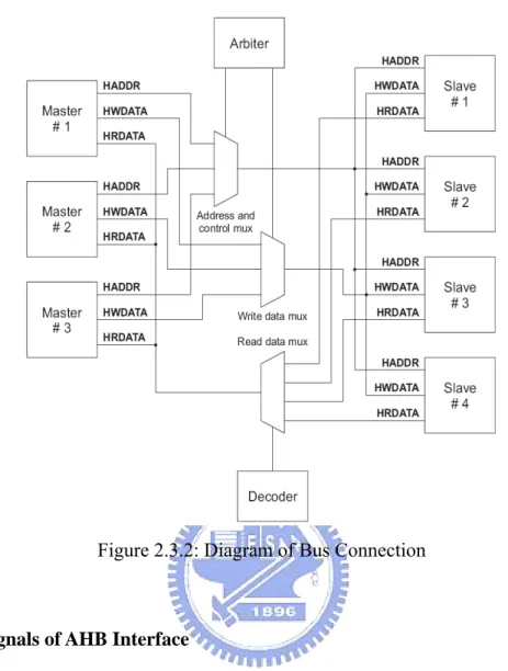
(26) Chapter 2 Background. ¾ AHB arbiter The existence of AHB arbiter means the multiple AHB masters and slaves are available in the AHB system. The AHB arbiter has the responsibility to ensure that only one bus master at a time is permitted to initiate data transfers. Even though the arbitration protocol is fixed, any arbitration algorithm, such as highest priority or fair access can be implemented depending on the application requirements. The AHB would include only one arbiter, although this would be trivial in single bus master systems. ¾ AHB decoder The AHB decoder is used to decode by address of each transfer and provide a signal to select which slaves that is involved in the transfer. A single centralized decoder is required in all AHB implementations. In the following subsection, the bus connection, signals of AHB interface, basic transfer, transfer type, and burst operation will be presented. The other details about arbitration will be in the AMBA specification. 2.3.2. Bus Connection. The AMBA AHB bus protocol is designed to be used with a central multiplexer interconnection scheme rather than the tri-state interconnection method, as shown in Figure 2.3.2. By using this scheme, all bus masters drive out the address and control signals indicating the transfer they wish to perform. Then, the arbiter receives the information from masters and determines which one has the ability to get the access privilege. Then, the master routes address and control signals to all of the slaves. However, only one slave will start to be accessed by the signal from arbiter. A central decoder is required to handle the necessary control of reading data and multiplexer to response correct signal, which selects the appropriate signals from the slave that is involved in the transfer.. - 16 -.
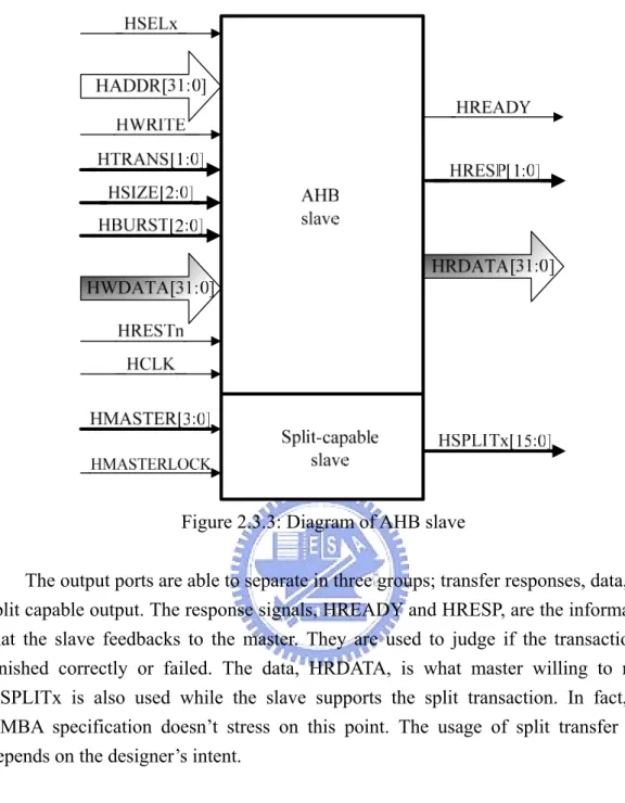
(27) Chapter 2 Background. Figure 2.3.2: Diagram of Bus Connection. 2.3.3. Signals of AHB Interface. The diagram of AHB slave is depicted in Figure 2.3.3. It shows total input and output ports. The bandwidth demonstrates here is 32 bits. Actually, the AMBA system is flexible to other bandwidth, such as 64, 128, or more bits are possible. The input ports could be divided into six groups according to its functionality; select, address and control, data, reset, clock, and split capable input. The select signal, HSELx, is from the arbiter to enable AHB slave to work. The address and control signals, HADDR, HTRANS, HSIZE, and HBURST, are together from AHB master. The master forwards the requirements to slave depending on these two kinds of information. Details will be presented in the following section. The data, HWDATA, clock, HCLK, and reset, HRESTn, are the common signals as we know. The last one group only exists in split capable slave. This group of signals is used to support the split transaction.. - 17 -.
(28) Chapter 2 Background. Figure 2.3.3: Diagram of AHB slave The output ports are able to separate in three groups; transfer responses, data, and split capable output. The response signals, HREADY and HRESP, are the information that the slave feedbacks to the master. They are used to judge if the transaction is finished correctly or failed. The data, HRDATA, is what master willing to read. HSPLITx is also used while the slave supports the split transaction. In fact, the AMBA specification doesn’t stress on this point. The usage of split transfer type depends on the designer’s intent. 2.3.4. Address Decoding. The signal HSELx is used to enable slave and is provided by the decoder, as shown in Figure 2.3.4. The decoder decodes the high-order address signals and then chooses one of the slaves to active. The minimum address space that can be allocated to a single slave is 1kB. All bus masters are designed such that they will not perform incrementing transfers over a 1kB boundary, thus ensuring that a burst never crosses an address decode boundary.. - 18 -.
(29) Chapter 2 Background. Figure 2.3.4: Signals to Select Which Slave 2.3.5. Basic Transfer. The transfer of AHB protocol is based on the pipeline operation. It separates the data and address phase into two stages, as shown in Figure 2.3.5. The necessary information including the HADDR and control, which are HADDR, HBURST, HSIZE, HTRANS, and HWRITE, will be broadcasted by master in the first stage. The second stage is data phase that passes or receives data in several cycles depending on the HRADY and HRESP.. Figure 2.3.5: Simple Transfer - 19 -.
(30) Chapter 2 Background. The HRADY indicates the transfer state. The logic high represents that it is ready to be finished and the logic low is contrast to be extended. Figure 2.3.6 is the example that the transfer is extended with two cycles. The first stage is address phase the same as shown in Figure 2.3.5. However, in the second stage, the logic low for HREADY means the transfer is not ready to be completed. This may result from both master and slave depends on the transfer type, HTRANS. It will be introduced in the later. Therefore, by using the HREADY, the transfer is lengthened to ensure the transaction could be terminated with expected results. 2.3.6. Transfer Type. Every transfer can be classified into one of four different types, as indicated by the HTRANS[1:0] signals. They are IDLE, BUSY, NONSEQ, and SEQ and controlled by 2’b00, 2’b01, 2’b10, and 2’b11 respectively. They are listed as below. ¾ IDLE It indicates that no data transfer is required and is used when a bus master is granted the bus, but does not wish to perform a data transfer. Slaves must always provide a zero wait state OKAY response to IDLE transfers and the transfer should be ignored by the slave.. Figure 2.3.6: Transfer with Two Wait. - 20 -.
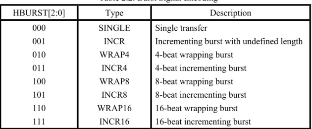
(31) Chapter 2 Background. ¾ BUSY The BUSY transfer type allows bus masters to insert idle cycles in the middle of bursts of transfers. This transfer type is used while the bus master is continuing with a burst of transfers, but the next transfer cannot take place immediately. When a master uses the BUSY transfer type the address and control signals must reflect the next transfer in the burst. The transfer should be ignored by the slave. Slaves must always provide a zero wait state OKAY response, in the same way that they respond to IDLE transfers. ¾ NONSEQ This transfer type represents the first transfer of a burst or a single transfer. The address and control signals are unrelated to the previous transfer. Because single transfers on the bus are treated as bursts of one, therefore the transfer type is also NONSEQUENTIAL. ¾ SEQ The remaining transfers in a burst are SEQUENTIAL and the address must be related to the previous transfer. The control information is identical to the previous transfer. The address is equal to the address of the previous transfer plus the size (in bytes) in the incrementing burst. In the case of a wrapping burst, the address of the transfer wraps at the address boundary equal to the size (in bytes) multiplied by the number of beats in the transfer (either 4, 8 or 16). 2.3.7. Burst Operation. Burst information is provided by the use of HBURST and the eight possible types are shown in Table 2.2. Incrementing burst is the sequential access of locations and the address of each transfer in the burst is just an increment of the previous address depends on the transfer size. For wrapping burst transfers, if the address of the first transfer is not aligned to the total number of bytes in the burst (size x beats), then the address of the transfers in the burst will wrap when the boundary is reached. For example, a four-beat wrapping burst of word (4-byte) accesses will wrap at 16-byte boundaries. Therefore, if the start address of the transfer is 0x34, then it consists of four transfers to addresses 0x34, - 21 -.
(32) Chapter 2 Background. 0x38, 0x3C and 0x30. The last transfer will wrap back to 0x30. As shown in Figure 2.3.7, the read rectangular is the incrementing burst and the blue rectangular is the wrapping burst which is depicted as the blue arrow. Table 2.2: Burst Signal Encoding HBURST[2:0]. Type. Description. 000 001 010 011 100 101 110 111. SINGLE INCR WRAP4 INCR4 WRAP8 INCR8 WRAP16 INCR16. Single transfer Incrementing burst with undefined length 4-beat wrapping burst 4-beat incrementing burst 8-beat wrapping burst 8-beat incrementing burst 16-beat wrapping burst 16-beat incrementing burst. The transfer size is controlled by HSIZE and supports eight dimensions; 8, 16, 32, 64, 128, 256, 512, and 1024 bits. It thus may suffer issues of alignment, as shown in table 2.3 and 2.4. The selection between big-endian and little-endian are defined in the specification directly and depend on the designer’s decision. As long as the designs all follow the same endian, it will not be a serous problem.. Figure 2.3.7: Two Kinds of Burst Operation. - 22 -.
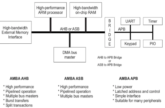
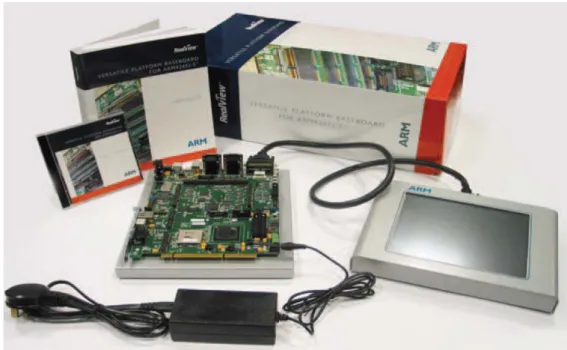
(33) Chapter 2 Background. Table 2.3: Active Byte Lanes for a 32-bit Little-Endian Data Bus Transfer size. Address offset. Data [31:24]. Data [23:16]. Data [15:8]. Data [7:0]. Word Halfword Halfword Byte Byte Byte Byte. 0 0 2 0 1 2 3. ˇ. ˇ. ˇ. ˇ. ˇ ˇ. ˇ ˇ. ˇ. ˇ. ˇ. ˇ. -. -. -. Table 2.4: Active Byte Lanes for a 32-bit Big-Endian Data Bus Transfer size. Address offset. Data [31:24]. Data [23:16]. Data [15:8]. Data [7:0]. Word Halfword Halfword Byte Byte Byte Byte. 0 0 2 0 1 2 3. ˇ ˇ ˇ. ˇ ˇ -. ˇ ˇ. ˇ -. ˇ. ˇ ˇ -. -. -. -. ˇ. 2.4 Overview of Emulation Environment In this thesis, the protocol verification is by the RealView Versatile Platform Basebord for ARM92EJ-S (VPB926EJ-S), as shown in Figure 2.4.1 [20]. It is the first basebord in the Versatile family and is designed for ASIC emulation and prototyping. By using the basebord, it takes great advantage of verifying validity of AMBA protocol, reducing the overall time about integrating our IP with others, and finally running real media applications on it.. - 23 -.
(34) Chapter 2 Background. Figure 2.4.1: Versatile Platform Baseboard for ARM926EJ-S This baseboard is designed specifically for ASIC emulation and prototyping, and supports advanced 3D graphics application development around ARM and PowerVR MBX cores. It also provides an AMBA Multi-layer AHB prototyping environment. Thus, we can prototype our design to verify the correctness of protocol. The architecture is shown in Figure 2.4.2. The upper part in the Figure is a powerful processing core; development chip. It can integrate high performance IP such as memory and DMA controllers and the ARM VFP9-S coprocessor around the ARM926EJ-S core. The vector processing capability of the ARM VFP9-S coprocessor offers increased performance for imaging applications such as scaling, 2D and 3D transforms, font generation, and digital filters. The development chip also includes an implementation of the ARM MOVE coprocessor which significantly improves the motion estimation capability required for applications like MPEG encode through hardware assistance for sum-of-absolute differences (SAD) calculations. The bottom part is the FPGA and it can be expended with logic tile. They are the programmable parts for HDL languages and share a common bus to communicate with other peripherals such as USB, I/O, Mse, Kbd, and etc. One different feature of the logic tile compared to FPGA is that it is able to communicate with on-chip memory as well as development chip. As a result, the logic tile, that we select is LT-XC2V8000 [21], is also needed for possible development in the future. It is a Virtex-II FPGA product of Xilinx and supports up to 8M gate counts. The detail information can be found in their individual document.. - 24 -.
(35) Chapter 2 Background. Figure 2.4.2: Architecture of Versatile Platform Baseboard. 2.5 Summary We have introduced four background references to finish this thesis. These references include the reasons, related knowledge, and verificated ways to design our IP for media applications. The first two are a reconfigurable architecture for media applications and design methodology. According this two references, we thus propose our designed IP. As a result, there is a overview about the protocol of our proposed IP in the following. Then, the last one is about the enmulation environment that is used to verify the correctness of protocol for our design.. - 25 -.
(36) Chapter 3 Design and Implementation of an ALU Cluster Intellectual Property. CHAPTER. 3. Design and Implementation of an ALU Cluster Intellectual Property According to the previous two chapters, the motivation and necessary background are viewed. Thus, the design and implementation of proposedd ALU cluster IP will be shown up in this chapter. Our IP consists of AHB slave wrapper, ALU cluster, and memory. Memory is the easiest component and can be instanced from memory compiler. Thus, it will not be mentioned frequently in this chpater. The design and implementation of the other two components are the key points in this chapter. The first section is the demonstration of the previous ALU cluster. It has been tapped out by UMC with 0.18 um process and Artisan design kit. Therefore, the die photo and summary of characteristics are listed in the beginning. The chip is then tested by Agilent’s tools. Through the testing of real silicon, it is convinced that the ALU cluster is practicable to handle media applications. The second section is about the design of the AHB slave wrapper which stands for interface between ALU cluster and AMBA bus. It will accept control signals from AMBA bus and manage the ALU cluster to execute its function. It is then programmed into the ARM series baseboard for hardware emulation. This will verify the correctness of protocol of the proposed AHB slave wrapper. The third section is about the ALU cluster IP that is a complete integration of improved ALU cluster and designed AHB slave wrapper together. The improved ALU cluster is referenced from first section and is designed and implemented to advance its performance. The results of simulation will be introduced then. After the successful - 26 -.
(37) Chapter 3 Design and Implementation of an ALU Cluster Intellectual Property. integration, a synthesizable IP is finished. Then, there is one extension of this IP. The main core of our IP is unchanged and the data memory is replaced by a novel storage, magnetic RAM (MRAM). The last two sections are the implementation comparisions and summary about the development. 3.1 An ALU Cluster The first part of this section is the brief report of the previous design, an ALU cluster, including the architecture, related layout, pad assignment and floorplan, die photo, and circuit summary. The testing is in the second part. It contains the testing environment, testing flow, and testing results. After the chip is tested, the ALU cluster is convincible that it is able to handle media applications as we expect. 3.1.1. Architecture of an ALU cluster. The architecture of an ALU cluster is shown in Figure 3.1.1. It consists of two ALU of two-stage pipeline, two multipliers of four-stage pipeline, one divider taking sixteen cycles to finish operation, a scratch pad register file (SPRF), ten banks of intra register file, a controller, and a decoder. The ALU can execute up to thirteen instructions; they are ADD, SUB, ABS, AND, OR, XOR, NOT, SLL, SRL, SRA, LT, GT, and EQ. The MUL can perform multiplication. The DIV can carry out three jobs: they are division that gets the quotient and remainder and find the square root. There are intra register files (IRF) embedded in the operation unit. The IRF are registers local to the operation unit. They can store streaming temporary. The SPRF is used to store coefficients using in common media applications and is used by ALU, MUL, and DIV to communicate with each other.. Figure 3.1.1: Architecture of an ALU Cluster - 27 -.
(38) Chapter 3 Design and Implementation of an ALU Cluster Intellectual Property. The decoder can parse the instructions and provides control signals to control the ALU cluster. When the ALU cluster in working state, the controller decides which input sources, IRF, SPRF, and data memory, to the functional unit. When it works in reading or writing state, the controller manages the data flowing to or from IRF, SPRF, and outer data memory. 3.1.2. Implementation Results. The summary of the circuit characteristics of the ALU cluster is listed in Table 3.1. The 0.18 um process of UMC and cell based design kit of Artisan are utilized for the implementation. The operating frequency of post-layout simulation is 100 MHz. The chip size and core size are about 3x3 mm2 and 2.2x2.2 mm2. The gate count of the core is 411491. It contains fifteen banks of memory for data and instruction. They are four 32 x 128 single port static RAM (SRAM), one 14 x 128 single port SRAM, and ten 32 x 32 single port SRAM. They are generated by memory compiler with Artisan library. The memory of 128 entries is used for instruction memory and they could support output bandwidth of 142 bits per cycle to the VLIW instructions. The data memory has ten banks and each bank has 32 entries. They can work together to provide up to the bandwidth of 320 bits per cycle. The power dissipation is 968.35 mW for the total chip when runs the media example of FIR filter that will have been introduced in the first chapter. The pure core size without these two kinds of memory is about 1.8 x 1.2 mm2. Its gate count is 255669 and the power is down to 312.38mW. The physical layout of the ALU cluster is shown in Figure 3.1.2. The core utilization is close to 88.8%. The data memory is the bottom rectangular and the instruction memory is the left rectangular. It can be seen clearly in Figure 3.1.3 about the floorplane and the pad assignment. There are total 127input/output (I/O) pads, where 47 input pads, 32 output pads, and 48 power pads. The die microphotograph is shown in Figure 3.1.4. It is packaged with CQFP128 and its photograph is shown in Figure 3.1.5. - 28 -.
(39) Chapter 3 Design and Implementation of an ALU Cluster Intellectual Property. Figure 3.1.2: Layout of an ALU cluster Table 3.1: Summary of an ALU Cluster Process. UMC 0.18 um. Library. Artisan SAGE-x Standard Cell Library. Post-layout Clock Rate. 100 MHz. Chip Size. 2.98 x 2.98 mm2. Core Size (without memory). 2.2 x 2.2 mm2(1.8 x 1.2 mm2). Gate Count (without memory). 411491 (255669). Power Dissipation (without memory). 968.35 mW (312.38 mW). On-chip memory. 10 32x32 single port SRMA 4 32x128 single port SRMA 14x128 single port SRAM. Pad. Input: 47 pins Output: 32 pins Power: 48 pins. - 29 -.
(40) d_24. d_23. d_22. d_21. d_20. d_19. core_vdd_07. io_vdd_3. core_gnd_07. io_gnd_3. core_vdd_06. d_18. core_gnd_06. d_17. d_16. d_15. d_14. d_13. d_12. core_vdd_05. io_vdd_2. core_gnd_05. io_gnd_2. core_vdd_04. d_11. core_gnd_04. d_9. d_10. d_8. d_7. d_6. CornerUL. d_5. Chapter 3 Design and Implementation of an ALU Cluster Intellectual Property. CornerUR. d_4. q_12. d_3. q_11. d_2. q_10. d_1. q_9. d_0. q_8. core_vdd_03. q_7. core_gnd_03. q_6. io_vdd_1. core_vdd_08. io_gnd_1. core_gnd_08. core_vdd_02. io_vdd_4. core_gnd_02. io_gnd_4. a_6. core_vdd_09. ALU cluster. a_5. core_gnd_09. q_5. a_3. q_4. a_2. q_3. Instruction Memory. a_4. a_1 a_0 core_vdd_01 core_gnd_01. io_vdd_0 io_gnd_0 core_vdd_00 core_gnd_00. mem_d_ctrl mem_d_wr. q_2 q_1 q_0 core_vdd_10 core_gnd_10. io_vdd_5 io_gnd_5 core_vdd_11 core_gnd_11. d_31. Data Memory. sel_3. d_30. q_13. q_14. q_15. q_16. q_17. q_18. q_19. core_vdd_12. core_gnd_12. io_vdd_6. io_gnd_6. core_vdd_13. core_gnd_13. q_20. q_21. q_22. q_23. q_24. q_25. core_vdd_14. core_gnd_14. io_vdd_7. io_gnd_7. core_vdd_15. q_26. CornerLL. core_gnd_15. d_25. q_27. d_26. clk. q_28. d_27. reset. q_29. d_28. sel_0. q_30. d_29. sel_1. q_31. sel_2. CornerLR. Figure 3.1.3: Floorplan and Pad Assignment of an ALU Cluster. Figure 3.1.4: Die Micro photo of an ALU Cluster. - 30 -.
(41) Chapter 3 Design and Implementation of an ALU Cluster Intellectual Property. Figure 3.1.5: Package of an ALU Cluster 3.1.3. Chip testing. There are two main testing targets for the chip of the ALU cluster; they are functionality and performance. The testing of functionality is divided into three parts which are memory, instruction, and real program testing. The performance testing is by the 16-tap FIR filter. The memory testing is divided into five stages as listed bellow. The purpose of using these five stages is to find out the possibility of stuck at one and stuck at zero failures. Isolating the memory testing is because memory is the most common failure part of the chip. ¾ ¾ ¾ ¾ ¾. Write all memory 32’hFFFF-FFFF, and then read them. Write all memory 32’h0000-0000, and then read them. Write all memory 32’hAAAA-AAAA, and then read them. Write all memory 32’h5555-5555, and then read them. Write all memory with interleaving 32’hAAAA-AAAA and 32’h5555-5555, and then read them.. All bits of memory are written by one and zero in the first two stages. In the third stage, one and zero in interleaving manner are written to the memory. The fourth stage is the opposite of the third stage which are zero and one instead of one and zero. Two continuous data with 32’hAAAA-AAAA and 32’h5555-5555 are written in the fifth stage. This stage cause the continuous data is interleaving with one and zero. - 31 -.
(42) Chapter 3 Design and Implementation of an ALU Cluster Intellectual Property. We then test functionality of instruction by feeding the random sources into all operational units. All instructions of different operation units must be gone through at least once to ensure the correctness. The last testing target is the real program by using 16-tap FIR filter as testbench that is the same benchmark of performance testing. The details will be in Appendix A. 3.1.3.1 Testing environment The environment for the chip testing is shown in Figure 3.1.6 and Figure 3.1.7. The chip is placed on the PCB board as shown in Figure 3.1.6. Most of the pins are placed in the order sequence that helps to chip testing. Figure 3.1.7 shows what environment we use. It is Agilent 16902A Logic Analysis System together with Agilent 16720A pattern generator and Agilent 16910A logic analyzer module [22]. This logic analyzer system can support up to 48 pins’ pattern input from the pattern generator module and catch up to 64 pins’ output results by logic analyzer module. The maximum frequency support to half pins’ usage of the pattern generator is 300MHz and 180MHz in full pins’ usage. It thus is adequate for the testing of our chip.. Figure 3.1.6: ALU Cluster on the PCB board. - 32 -.
(43) Chapter 3 Design and Implementation of an ALU Cluster Intellectual Property. Figure 3.1.7: Logic Analyzer System with LCD Monitor Display 3.1.3.2 Testing flow and results The testing flow is shown in Figure 3.1.8. It is divided into three stages. The first stage is in the upper rectangular for preparing test pattern. Because the visibility of chip testing is very low, it is not easy to judge the sources of the problems. We thus run the testing target at the software level simulation to avoid the possibility of invalid testing pattern. The simulation results are then record and prepared to be compared with the outcomes of chip testing. The necessary format of test pattern for the pattern generator is produced with the simulation at the same time. The second stage is in the middle rectangular that is chip testing in the Logic Analysis System. The pattern generator module produces the same stimulus as simulation for the chip and then the logic analyzer module receives the results after chip processes the incomes. Therefore, the fruits from the logic analyzer module are compared with the ones from simulation in the third stage. After the outcomes are compared between software simulation and hardware testing, the results are listed, as shown in Table 3.2. The clock rate of memory and instruction testing is lower down to 1MHz for simplifying the possible problems from chip. Through the testing flow, we make sure that all the memory banks including data and instruction memory are correct. Also, the instructions of different functional units are true. The outcomes of program of FIR filter system are correct, too. - 33 -.
(44) Chapter 3 Design and Implementation of an ALU Cluster Intellectual Property. Figure 3.1.8: Testing flow of chip level testing Table 3.2: Testing Results Memory. Instruction Functionality. FIR. Data. Correct. Instruction. Correct. ALU0. Correct. ALU1. Correct. MUL0. Correct. MUL1. Correct. DIV0. Correct. Correct around 16~18 MHz. However, the performance of the FIR filter system is down to around sixteen to eighteen MHz. It is more than five times slower than the post-layout simulation. The reason of this performance loss is because of the large loading through the probe lead set and the PCB board. It reminds us that it is necessary to connect the pod of Agilent to the chip directly in the future. Otherwise, it is hard to get the true performance of the chip from the huge loading.. - 34 -.
(45) Chapter 3 Design and Implementation of an ALU Cluster Intellectual Property. 3.2 Design and Emulation for the AHB Slave Wrapper of Intellectual Property In this section, there are three parts to demonstrate the design and hardware emulation. The architecture of the AHB slave wrapper is showed first. It shows up the functionality of the wrapper and how it controls the ALU cluster to execute media applications by finite state machine. Then, it will be programmed into ARM series baseboard to proceed hardware emulation for verifying its protocol. However, there are some necessary modifications for the baseboard, it will be displayed in the second pats. The last one is the emulation results. According to the hardware emulation, we can make sure that the correctness of protocol for proposed wrapper is verified. 3.2.1. Architecture of AHB Slave Wrapper. The architecture of the proposed wrapper consists of two components that are finite state machine (FSM) and address generation unit (AGU), as shown in Figure 3.2.1. The FSM is in charge of receiving the signals from the AMBA bus and administrating the IP to obey the protocol of AHB slave. It will tell the AGU to produce the necessary address weather the ALU cluster is accessed in bursting incrementing or wrapping mode. There is one signal, alu_work, from the ALU cluster to FSM. It will be used to identify if the ALU cluster finishes executing the media applications or not. With the necessary information from the AMBA bus and ALU cluster, the FSM just can control the ALU cluster including, write data, read data, and execute instruction.. Figure 3.2.1: Architecture of AHB Slave Wrapper - 35 -.
(46) Chapter 3 Design and Implementation of an ALU Cluster Intellectual Property. 3.2.1.1. Finite State Machine of AHB Slave Wrapper. The FSM of the wrapper is used to control the states of the IP and response the request of AMBA bus, which is used to dealing with issues such as reading and writing with on-chip bus and activating the ALU cluster. It has the responsibility to ensure that the IP is able to communicate with other modules from the AMBA bus. As a result, it must have some prescribed response back to AMBA bus. Also, it will identify the input signals from the AMBA bus and tell the ALU cluster if it has to execute the applications or still in its original state. Therefore, the FSM is designed with six states; they are Idle, Accessible, ALU_Work, Un-readable Wait, Un-writable Wait, and Error, as shown in Figure 3.2.2. ¾. Idle:. When the IP is not accessed and the ALU cluster finishes its executing, the FSM will be in the Idle state. It will go to other states while the bus is granted and the IP will be accessed or the ALU cluster is activated. Not only until IP has done the employment but also suffers some error, it will come back to the Idle state. In this state the wrapper will be ready to get the signals from AMBA bus and prepare next work. Basically, only while the HTRANS is equal to NONSEQ, it has the chances to move to other states. Otherwise, it will keep the Idle state. If the NONSEQ signal is encountered, it identifies which operation the IP is requested by HWRITE. Then, the FSM can move to its target state. ¾. Accessible. The FSM will directly move to Accessible state if the HTRANS is equal to NONSEQ and HERITE is high. In the Accessible state, the FSM continuously checks if the IP is accessed repeatedly. It will be two different kinds of accessing, but cause FSM still in the Accessible state. One of them is that HTRANS is still equal to NONSEQ. It means the the IP is accessed with different address. The other is that HTRANS is equal to SEQ. It represents that previous access is continuous with burst mode of wrapping or incrementing manner. There are three cases that the FSM will move away; the HTRANS changes to IDLE or BUSY and the reading data is not ready. These three cases mean that the access is finished, busy to write, and ready to read but data is not ready and will induce the state move to Idle, Un-readable Wait, and Un-writable Wait, respectively. - 36 -.
(47) Chapter 3 Design and Implementation of an ALU Cluster Intellectual Property. Figure 3.2.2: Finite State Machine ¾. Un-readable Wait. There are two possible paths that FSM will enter the Un-readable Wait state. One of the two paths is while the FSM is in the Idle state and the TRANS is NONSEQ and the HWRITE is low. It means the IP is being read. However, the first reading operation needs two cycles to prepare necessary data. Thus it must be in the Un-readable Wait state to wait the data. Until the data is ready, the FSM moves to Accessible state to carry out the following reading request. The other path is from Accessible state to Un-readable Wait state. The reason that the FSM must move to this state is the same as the first path, the necessary latencies. ¾. Un-writable Wait. There is only one reason that will enforce the FSM move to Un-writable Wait state. It is when the IP is being written data in burst mode of wrapping or incrementing way, but the TRANS is changed to BUSY. Pending the TRANS changes back to NONSEQ or SEQ, the FSM will return to Accessible state. ¾. Error. The FSM will go to the Error state while the IP is accessed in wrong ways. They are invalid address and invalid transaction. The invalid address is because the depth of - 37 -.
(48) Chapter 3 Design and Implementation of an ALU Cluster Intellectual Property. the data and instruction memory is limited. If the depth is over the real memory, it will be found by the FSM and go to the Error state. The invalid transaction is to avoiding the wrong combinations of HTRANS that violates the AHB protocol, although this might not be happened. The Error state will also occur if the IP is being accessed and is not granted unexpectedly, controlled by HSEL. This is designed to provide ability against accident. If the Error occurs, the Error state must obey the AHB protocol and thus have two cycles response, replying the AMBA BUS with proper HRESP and HREADY as defined in the specification. ¾. ALU_Work. The ALU_Work state manifests the IP is in the working service. The ALU cluster executes applications according to the instructions. There is only one path going to this state that is from Idle state to this one. The ALU cluster will be invoked by a strictly method that is to write the IP the end value of the program counter at predefined location. The details will be in Appendix B. In this state, if the wrapper is accessed weather it is a reading or writing operation, the FSM has the ability to reply the two cycles responses, RETRY, to the AMBA bus. At the same time, the ALU cluster keep working without being affected by the unexpected access until the end of the application. It will have internal check in the ALU cluster to judge if the execution is finished. Then, through signal, alu_work, the wrapper gets the status of ALU cluster. There is one thing needed to be emphasized. Because the execution must go through many stages to finish one instruction, it will take more cycles to write back the executed results. The extra cycles are depending on the different functional units. For example, the ALU is a two stages pipeline functional unit so that it takes six cycles that is two plus four to finish its operation. The four cycles is necessary course for every operation, such as instruction decoding, data source selecting, and result writing. Thus, the four stages functional unit, MUL, will take eight cycles and the sixteen cycles’ functional unit, DIV, will take twenty cycles to write back the result. 3.2.2. Modifications for Baseboard and Data Preparing. There are some modifications needed to program our wrapper into the baseboard. One of them is the interface of the wrapper to the outer bus because of the mismatch of the communication bus between the wrapper and baseboard. It can be found in the document of the baseboard that the data ports through the AHB bridges are shared by - 38 -.
(49) Chapter 3 Design and Implementation of an ALU Cluster Intellectual Property. writing and reading data signals. Thus, data signals of the wrapper to outer bus must be replaced with single tri-state bus, as shown in Figure 3.2.3. When the IP is accessed as writing transaction, it stands for input ports. As for reading state, the share bus then becomes output ports. It is needless of any revision for other ports because the baseboard is originally designed to be able compatible with AMBA system.. Figure 3.2.3: Ports modification Because programming ALU cluster into the baseboard is hardly to verify the performance due to huge system, the baseboard doesn’t contain enough memory, and the functionality of the ALU cluster is verified through silicon, it is not necessary to program total IP into the baseboard. Thus, we take off the ALU cluster, instruction memory, and data memory and replace them as register files, as shown in Figure 3.2.4. Notice that only the wrapper and register files are prepared to be programmed into the baseboard. The register files are used to store the accessed results and return them back by the wrapper with the on-chip bus. The connections to the register files have taken the place of the ones to original ALU cluster. As to the signal alu_work, it is tied to high that represents the ALU cluster is unused. Thus, this modification can simplify the effort of protocol verification by only access the register files through the wrapper. There are also many data needed to be programmed into the baseboard with our wrapper together. They are Arbiter, Decoder, and Multiplexer. These components are used to select control the AMBA bus. All of them are ready and can be got from ARM’s website. Thus, we put all these components including our wrapper and register files to software of Xinlinx ISE to do board level synthesis, placement, and routing [23]. After the software is finished, the programming bit file is then generated. With the bit file, we therefore can use the ARM Multi-ICE to program it into the baseboard [24].. - 39 -.
(50) Chapter 3 Design and Implementation of an ALU Cluster Intellectual Property. Figure 3.2.4: Modifications with Added Register Files 3.2.3. Emulation Result. After successfully programming our wrapper into the baseboard, the software of ARM Developer Suite (ADS) is then used to proceed the emulation [25]. By the ADS, the software codes are then assembled, compiled, and linked to be able to control the communications between ARM core and our wrapper. The software codes are demonstrated in Figure 3.2.5 and Figure 3.2.6. Figure 3.2.5 is the simple C code that has 32 entries of integer array that store 32 constants. These constants are then written to the specific address, ACT_ADD, which is the address of our wrapper and then read them out. The address is defined in Figure 3.2.6. WRAPPER_BASE is the base address of the wrapper and WORD_OFFSET is the offset to execute word access. Then, the read and written constants are compared to ensure that correctness of the transaction between ARM core and wrapper. The results are shown in Figure 3.2.7. It lists all the written and read results and comparison. After the successful emulation, we therefore can make sure our wrapper is verified through the baseboard and is able to be integrated with other existing IP. Besides, the flow of emulation is set up from FPGA synthesis to ADS emulation. This flow is reusable to further ARM series development in the future.. - 40 -.
(51) Chapter 3 Design and Implementation of an ALU Cluster Intellectual Property. Figure 3.2.5: Software codes for ADS. Figure 3.2.6: Address Definition. - 41 -.
(52) Chapter 3 Design and Implementation of an ALU Cluster Intellectual Property. Figure 3.2.7: Emulation Results. 3.3 An ALU Cluster Intellectual Property In this section, we combine the improved ALU cluster and designed wrapper together. The improvement of the ALU cluster is for control and internal storages. As for the operational units, they are the same with old ones. It will be showed in the first part in this section. The second part is about the functional simulation. The testbench is 16-tap FIR program that is one common media application. Then, the last part is the summary of the improvements. 3.3.1. Architecture of an ALU Cluster Intellectual Property. The architecture of IP consists of the wrapper, ALU cluster, instruction memory and data memory, as shown in Figure 3.3.1. The wrapper is introduced in previous section. The decoder in the ALU cluster is the main improvement. One of the improvements is to improving the ability of reading source and writing destination. It makes all memory, including data and instruction memory, expose to the AMBA bus. They can be accessed directly from AMBA bus. Besides, it betters the performance in shortening access cycles. The reading takes two cycle’s latencies in bursting reading. After the latencies, the reading data comes out every cycle. As for the orginal one, it must have four cycles to access one burst read. - 42 -.
(53) Chapter 3 Design and Implementation of an ALU Cluster Intellectual Property. 32 32 14 alu_work 32. 32. 32. 32. 14. 142. 142 7+3. 32 32*10 32*5 5+4. 32 32. 32 32. 32 32. 32 32. 32 32. Figure 3.3.1: Architecture of an ALU Cluster IP In order to let the ALU cluster is able to execute while AMBA bus is granted by other master, the ALU cluster needs a module that feeds instruction memory the address automatically. The new component, Pc_counter, is added to handle this job. It will increase the program counter by one every clock cycle. The decoder will have the end value of Pc_counter and compare it every cycle to check if the ALU cluster finishes the job. If the job is done, it actives the alu_work signal to let wrapper know the situation. If the alu_work is inactive, the IP can not be accessed simply and will return RETRY response back to AMBA bus. There is one special input combination can erase end value of Pc_counter in the decoder and thus coerce the IP to stop execution. This coercive mechanism is designed for avoiding possibility of deadlock occurring. 3.3.2. Functional Verification. The development of the IP including finite state machine in the wrapper and total architecture is shown as above. In this part, the simulation of the testbench of 16-tap FIR filter and its results will be demonstrated to verify the executing ability of the IP for media applications.. - 43 -.
數據
+7

![Table 2.4: Active Byte Lanes for a 32-bit Big-Endian Data Bus Transfer size Address offset Data [31:24] Data [23:16] Data [15:8] Data [7:0] Word 0 ˇ ˇ ˇ ˇ Halfword 0 ˇ ˇ - - Halfword 2 - - ˇ ˇ Byte 0 ˇ - - - Byte 1 - ˇ - - B](https://thumb-ap.123doks.com/thumbv2/9libinfo/8466163.183355/33.892.136.764.441.698/table-active-lanes-endian-transfer-address-halfword-halfword.webp)
相關文件
Instruction Set ...1-2 Ladder Diagram Instructions...1-2 ST Statement Instructions ...1-2 Sequence Input Instructions ...1-2 Sequence Output Instructions ...1-3 Sequence
[r]
Quality kindergarten education should be aligned with primary and secondary education in laying a firm foundation for the sustainable learning and growth of
[r]
[r]
[r]
In basic education, students acquire a foundation of knowledge, skills and values across Key Learning Areas. They also receive guidance and advice to help them make
• A sequence of numbers between 1 and d results in a walk on the graph if given the starting node.. – E.g., (1, 3, 2, 2, 1, 3) from
