行政院國家科學委員會專題研究計畫 成果報告
異質整合 Mixed-signal/MEMS CMOS 無線射頻收發機設計研
發--子計畫二:可重組式 Mixed-signal/MEMS .9G~10GHz
射頻接收端設計(2/2)
研究成果報告(完整版)
計 畫 類 別 : 整合型 計 畫 編 號 : NSC 99-2220-E-009-041- 執 行 期 間 : 99 年 08 月 01 日至 100 年 07 月 31 日 執 行 單 位 : 國立交通大學電子工程學系及電子研究所 計 畫 主 持 人 : 郭建男 計畫參與人員: 碩士班研究生-兼任助理人員:林翰柏 碩士班研究生-兼任助理人員:張家愷 博士班研究生-兼任助理人員:曾冠豪 報 告 附 件 : 出席國際會議研究心得報告及發表論文 公 開 資 訊 : 本計畫涉及專利或其他智慧財產權,2 年後可公開查詢中 華 民 國 100 年 10 月 31 日
中文摘要: 在這個報告中,我們將呈現適合用於寬頻系統中的關鍵電路。 包含一個操作於1.3-5.3 GHz 的低雜訊放大器、一個輸出頻率是 3-5.7GHz 的三倍頻器、一個 1-5 GHz 的頻率-直流電壓轉換器、 一個DC-4.38 GHz 的寬頻時間延遲電路、一個 3-4 GHz 的相移 器。以上電路都是使用0.18-μm CMOS 的製程來設計與實現。 在寬頻低雜訊放大器的設計中,我們使用了基極交互耦合與電 容交互耦合兩個電路技巧,這兩個技巧不只增加的電路的增益 與線性度,也抑制了雜訊指數。此電路的3 dB 頻寬為 1.27-5.31 GHz。最大的差動增益是 10.13 dB。當輸入信號是 3 GHz 時,電路的P1dB 與 IIP3 分別是-10 dBm 和 0 dBm。此電路在 供應電壓是1.8 伏時,直流功率消耗是 7.32 mW。 為了產生寬頻的本地信號,我們設計了一個低功率且使用次諧 波混頻的四相位三倍頻器。當供應電壓是1.8 V 時,此三倍頻 器消耗了11.5 mW 的直流功率。當輸出信號是 4.5 GHz 時,本 電路的基頻諧波抑制比為35 dB 且轉換增益為-4.2 dB。 我們設計一個頻率-直流電壓轉換器來直接轉換輸入射頻訊號成 為輸出直流電壓。我們所提出的電路由頻率-功率轉換器與功率 偵測器所組合而成。其中頻率-功率轉換器是由四級的限制放大 器所組成。本電路可以不需降頻就直接把1-5 GHz 的輸入信號 輸出成0.22-1.42 V 的直流電壓,本電路的輸入功率範圍是-7 到 +5 dBm 之間。當供應電壓是 1.8V 時,本電路的直流消耗功率 是16.5 到 17.8 mW。 為了達到頻寬的延展,我們使用二階形式的Pade 近似電路來設 計一個平坦的時間延遲電路。由量測結果可以知道,本電路可 以在操作GHz 頻段時達到 49 psec 的時間延遲。當供應電壓是 1.8V 時,本電路的直流消耗功率是 7.88 mW。 為了相位陣列發射機系統的應用,我們設計了一個具有高輸入 功率範圍的相移器。當使用我們所提出的可調增益放大器在 I/Q 相位結合的相移器中時,輸出信號的特性將會大幅被改 善。從量測結果得知,即使輸入功率改變,增益的變化小於 1.5 dB 而相位失真小於±2 °。當供應電壓是 1.8 V 時,本電路的 最小直流消耗功率為15.46 mW。
英文摘要: In this report, several key circuit blocks for wideband receiver will be presented, including a 1.3-5.3 GHz wideband balun low-noise amplifier (LNA), a 3-5.7GHz frequency tripler, a 1-5GHz frequency to DC voltage converter (FVC), a DC-4.38 GHz wideband delay circuit and a 3-4 GHz phase shifter. All circuits are designed and implemented in 0.18-μm CMOS process.
In wideband LNA design, the bulk cross-coupling (BCC) and capacitance cross-coupling (CCC) techniques are introduced, which not only increase gain and linearity but also decrease noise figure.
The 3 dB bandwidth extends from 1.27 GHz to 5.31 GHz. The maximum differential gain is 10.13 dB. Measured at 3 GHz, P1dB and IIP3 are -10 dBm and 0 dBm, respectively. The LNA core circuit dissipates 7.32 mW from 1.8 V power supply.
A low-power quadrature frequency tripler using sub-harmonic mixing is designed for wideband LO signal generation. The
frequency tripler consumes 11.5mW from 1.8V supply voltage. The fundamental harmonic rejection ratio (HRR1) achieves more than 35 dB, and the conversion gain achieves -4.2 dB at output frequency of 4.5 GHz.
A frequency-to-voltage converter (FVC) is designed for directly converting an RF input signal to a DC output voltage over a wide microwave frequency range. The proposed circuit consists of a 4-stage limiting amplifier (LA) for frequency-to-power converter (FPC) and a power detector for power-to-voltage conversion. Consequently, the circuit converts the signal frequency of 1-5 GHz to the measured DC voltage of 0.22-1.42 V without the influence of the input power level from -7 to +5 dBm. With 1.8 V supply
voltage, the dc power consumption varies from 16.5 to 17.8 mW, depending on the input frequency.
A flat wideband delay circuit is designed using the 2nd-order form of the Pade approximant for bandwidth extension. The measured result shows that the circuit achieves a delay time of 49 psec in the GHz frequency range. The power consumption of the core circuit is 7.88 mW from 1.8 V supply voltage.
A high input power range phase shifter is designed and fabricated for phase array transmitter application. With proposed variable gain amplifier in I/Q vector combination based phase shifter, the
performance of output signal has been improved. From measured results, the gain variation and phase distortion versus input power of output signal are smaller than 1.5 dB and ±2 °, respectively. The minimum DC consumption of core circuit is 15.46 mW from 1.8 V supply voltage.
計畫名稱
異質整合 Mixed-signal/MEMS CMOS 無線射頻收發機設計研發 ---
子計畫二:可重組式 Mixed-signal/MEMS 0.9G~10GHz 射頻接收端
設計(2/2) Reconfigurable mixed-signal/MEMS 0.9G~10GHz Receiver
Design (2/2)
計畫編號:NSC
99-2220-E-009-041
主持人:
郭建男教授
單位:國立交通大學電子工程學系
Contents
Contents………. ii
Chapter 1 Introduction……….
1
Chapter 2 Design for Direct Down-Conversion Receiver……….
2
2.1 Introduction………
2
2.2 Design and Implementation of Wideband LNA………..
3
2.3 LNA Implement and Measurement Result………...…...
5
2.4 Design of Frequency Tripler for Wideband LO Generation……..
7
2.5 Measurement Result of Frequency Tripler for Wideband LO
Generation………..……..
9
2.6 Conclusion………...
10
Chapter 3 Circuit Blocks for Direct FSK Demodulator using
RFVC……….
11
3.2 Circuit Design of Radio-Frequency to DC Voltage Converter…...
12
3.3 Measurement Results of RFVC………
14
3.4 Conclusion………...
15
Chapter 4 Wideband Delay Circuit for Time Array System……. 16
4.1 Introduction………...
16
4.2 Circuits Design………...
17
4.3 Measurement results of Wideband Time Delay Circuit…………
20
4.4
Conclusions………21
Chapter 5 High Input Power Range Phase Shifter for
Transmitter Array Application………
22
5.1
Introduction………...22
5.2
Circuit Design………24
5.4
Conclusion………..29
Chapter 6 Conclusions and Future Works……….
30
6.1 Conclusions……….
30
6.2 Future Work………...
31
Reference……… 32
Chapter 1 Introduction
The trend for communication circuits has been moved to reconfigurable design for multi-standard applications. For this purpose, the circuit designer will meet the challenges for wide frequency operating range, large dynamic power range, multi- modulation schemes and so on.
Otherwise, with the progress of wireless communication techniques, the single antenna transceiver could not satisfy the requirement of advanced protocols. The beam-forming technique should be introduced in the future transceiver design. In this report, the crucial circuit blocks for wideband operation and beam-forming system will be designed, implemented and verified in CMOS technology.
This report is organized as follows. In Chapter 2, the circuit blocks design for direct down-conversion receiver will be presented. The circuit blocks for direct FSK demodulator using RFVC will be given in Chapter 3. For wideband beam-forming system design requirement, the key circuit blocks such as time delay circuit and phase shifter is developed and described in Chapter 4 and Chapter 5, respectively. Finally, a conclusion will be given in Chapter 6.
Chapter 2 Circuit Blocks Design for Direct Down-Conversion
Receiver
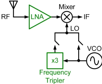
Fig. 2-1. Block diagram of direct down-conversion receiver
Fig. 2-2. Schematic of proposed wideband balun low noise amplifier
2.1 Introduction
Fig. 2-1 shows the block diagram of direct down-conversion receiver, which includes a wideband low-noise amplifier (LNA), a down-conversion mixer, a frequency tripler, and a voltage controlled oscillator (VCO). The design challenge in both signal path and signal source is the wide operating frequency range. In signal path, a wideband, high linearity balun LNA is proposed. Otherwise, the cascade of VCO and frequency tripler with switch control is proposed in signal source design. This solution will relax the frequency tuning range design of VCO. In this chapter, the design and measurement result of wideband LNA will be presented in Section 2.2 and Section 2.3, respectively. And the design and measurement result of frequency tripler will be given in Section 2.4 and Section 2.5, respectively. Finally, a conclusion is shown in Section 2.6.
2.2 Design and Implementation of Wideband LNA
The wideband balun LNA design needs to overcome several challenges. The first one is wideband input impedance matching. The second is gain enhancement to overcome signal loss under finite DC power consumption budget. The third is good linearity over the operating frequency band to avoid the effect of inter-modulation distortion on system performance.
The proposed schematic is shown in Fig. 2-2. The LNA circuit requires wideband input matching. In literature, the LC ladder matching network was implemented for the purpose [1]. We avoid this approach since the LC ladder topology occupies much chip area because of inductors.
Instead, we utilize the low input impedance feature of the common-gate stage of
M1, suitable for wideband input matching application. The input impedance is
dominated by M1 as 1/gm [5]. The input capacitance at node A gradually degrades the input return loss at high frequencies.
The device size shall be as small as possible. The size selection is really a trade-off between gain and input return loss. As compared to [2], the operating frequency in this design appears to be higher such that the effect by the input capacitance has more impact on the input impedance matching. The on-chip inductor L3 is therefore used to compensate for the parasitic capacitance so as to extend the bandwidth. Obviously the reactance cancellation occurs in a narrow band. This design makes 1/gm somewhat larger than 50 Ω, and the input impedance trace on the Smith chart circle around the center point of 50 Ω. Consequently, the impedance matched condition extends to a larger range in the sense of 10-dB return loss. L3 also provides a DC sink path to M1.
The balun function of wideband single-to-differential conversion is provided by the common-gate stage of M1 and the common-source stage of M2 [2]. The in-phase path is given by the common-gate stage, and the inverted phase path is provided by the common-source stage. The device size of M1 is limited to achieve 50 ohm input matching. For enlarging the total gain response of LNA, the device size of
M2 is larger than M1 in this work. For output gain balance consideration, the load
impedance of differential path in this work is not under symmetric design.
The cascode conFiguration is used for gain stage design in this LNA, which features better isolation between input and output ports. Two techniques are applied to boost the gain level of the balun LNA. The technique of bulk cross-coupling (BCC) is used, connecting the bulk node of M1 to the source of M2, and the bulk node of M2 to
the source of M1. This technique increases the equivalent transistor transconductanc
from gm to gm+gmb under the same DC dissipation condition, where gmb is the body
M3 M4
Vin
ZL1 ZL2
Vo
(a) (b)
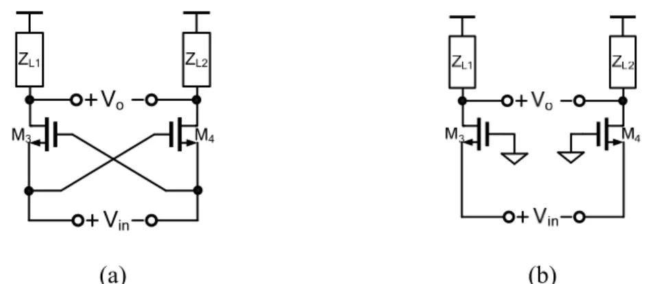
Fig. 2-3. Small signal model of (a) capacitance cross-coupling and (b) common- gate
The second technique for gain enhancement is capacitance cross-coupling (CCC) realized by M3, M4, C3, and C4. The small signal model is shown in Fig. 2-3(a). And
the common-gate (CG) conFiguration is also shown in Fig. 2-3(b) for comparison. Let the sizes of M3 and M4 be identical. The voltage gain of CCC and CG could be
derived as
(
1 2)
3 , m L L in o CCC v g Z Z V V A = = + (1)(
1 2)
3 , 2 1 L L m in o CG v g Z Z V V A = = + (2)From Eq. (1) and (2), the voltage gain ratio between CCC and CG are two. In other word, the CCC topology is more advantageous than the CG topology in gain/power efficiency. The performance of second-order distortion and noise are also improved by the CCC topology. More details can be found in [3].
2.3 LNA Implement and Measurement Result
The proposed wideband balun LNA was fabricated in 0.18-μm standard CMOS technology. Fig. 2-4 shows the die photo of the fabricated circuit. The total chip size, including core circuits and testing pads, is 1080 μm x 770 μm.
Fig. 2-4. Die photo
Fig. 2-5. Differential gain versus frequency
Fig. 2-6. Gain difference versus input frequency
Fig. 2-7. Phase balance versus input frequency
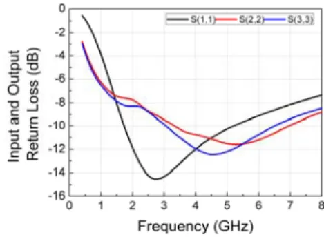
Fig. 2-8. Input and output matching
The differential gain is shown in Fig. 2-5. The maximum differential gain is 10.17 dB at 3.08 GHz, and the 3 dB bandwidth is from 1.27 GHz to 5.31 GHz. The gain and phase balance of proposed wideband balun LNA are shown in Fig. 2-6 and Fig. 2-7, respectively. The gain difference is smaller than ±1.5 dB from DC to 6 GHz. The phase balance is below ±12 degree at operation frequency band. Fig. 2-8 shows the input and output matching of proposed wideband balun LNA.
The input return loss is below -10 dB from 1.74 GHz to 5.2 GHz and the output return loss is below -10 dB from 3.34 GHz to 6.5 GHz. The wideband linearity test result includes P1dB and IIP3 are both shown in Fig. 2-9. The minimum P1dB is -10.67
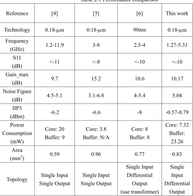
dBm at 4 GHz. The frequency offset for IIP3 setup is 1.0 MHz, and the minimum IIP3 is -0.57 dBm when input frequency is 2 GHz. Fig. 2-10 shows the measured noise Figure versus operating frequency. The noise Figure is below 5.5 dB from 2.1 GHz to 4.05 GHz, and the minimum value is 5.04 dB at 3.17 GHz. The performance summary and comparison is shown in Table 2-1.
Table 2-1 Performance comparison
Reference [4] [5] [6] This work
Technology 0.18-μm 0.18-μm 90nm 0.18-μm Frequency (GHz) 1.2-11.9 3-8 2.5-4 1.27-5.31 S11 (dB) <-11 <-8 <-10 <-10 Gain_max (dB) 9.7 15.2 10.6 10.17 Noise Figure (dB) 4.5-5.1 3.1-6.8 4-5.4 5.04 IIP3 (dBm) -6.2 -6.6 -8 -0.57-0.79 Power Consumption (mW) Core: 20 Buffer: 9 Core: 3.8 Buffer: N/A Core: 8 Buffer: 8 Core: 7.32 Buffer: 23.26 Area (mm2) 0.59 0.96 0.77 0.83
Topology Single Input Single Output Single Input Single Output Single Input Differential Output (use transformer) Single Input Differential Output
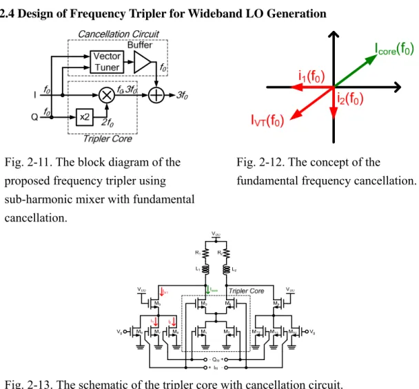
2.4 Design of Frequency Tripler for Wideband LO Generation
Fig. 2-11. The block diagram of the proposed frequency tripler using sub-harmonic mixer with fundamental cancellation.
Fig. 2-12. The concept of the
fundamental frequency cancellation.
Fig. 2-13. The schematic of the tripler core with cancellation circuit.
Fig. 2-11 shows the block diagram of the quadrature frequency tripler with fundamental cancellation. It consists of an I/Q-pair of the tripler cores and cancellation circuits.
The fundamental quadrature I/Q input signals at the frequency f0 are first used to
generate the second-order harmonics at 2f0 by frequency doublers. Then the doubler
outputs are mixed with the fundamentals to produce the quadrature third-order harmonic outputs at the frequency 3f0.
The output fundamental cancellation circuit is introduced to suppress the spur at the fundamental frequency to obtain a high HRR1value. The design concept is using vector tuner to generate an out of phase signal to null out the output fundamental frequency. The vector diagram cancellation mechanism is shown in Fig. 2-12.
The circuit schematic of the proposed frequency tripler using sub-harmonic mixing mechanism is shown in Fig. 2-13. The core circuit of the tripler is composed of frequency doubler and the mixer can be realized in a cascode conFiguration (M1-M4),
known as the sub-harmonic mixer. This current-reuse topology is advantageous in low power consumption. The bottom transistor pair (M1, M2) forms an efficient frequency
doubler. It generates the output current at to drive the top source-coupled differential pair (M3, M4), which works as the switching stage of the mixer. This mixer produces
the third-order harmonic by frequency up-conversion of current commutation.
Circuit operation relies on the second-order nonlinearity in both transistor pairs. To maximize the efficiency of frequency conversion, each transistor gate port is biased for the maximum voltage derivative of device transconductance.
The efficiency of frequency conversion also relies on the phase relationship of the two input signals to the upper and lower differential pairs. It is found the phase difference needs to be ±90 degrees out of phase, or a quadrature pair.
As shown in Fig. 2-13, the cancellation circuit is implemented in the differential form. It consists of a unit current gain buffer (M5 and M9) and a vector tuner (M7, 8
and M11, 12). Transistors (M6 and M10) work as current sources to provide appropriate
biasing current to the gain buffer. The gain buffer isolates the tripler and vector tuner to reduce the loading effect on the tripler core due to the parasitic capacitance from the vector tuners.
The output fundamental component of icore is due to the direct feed-through of the
input signal at the gate port of M4. The cancellation circuit generates cancellation
current Ivt of 180 degrees out of phase to null out that component. Ivt comes from the
vector combination of the input I and Q signals, which magnitudes are adjusted by M11 and M12, respectively, to produce the required phase and magnitude.
2.5 Measurement Result of Frequency Tripler for Wideband LO Generation
The tripler circuit with fundamental frequency cancellation is fabricated in 0.18 um CMOS technology. The microphotograph is shown in Fig. 14. The entire die area is 1.4x1.1 mm2 including pads, but the circuit only occupies 0.35x1.1 mm2 without the poly-phase filters.
Fig. 2-14. Microphotograph of the entire quadrature tripler.
Fig. 2-15. Harmonic rejection of the
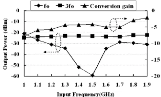
fundamental at 1.5 GHz Fig. 2-16. The output power and conversion gain
From measured result, the conversion voltage gain is -4.2 dB, excluding the loss due to the poly-phase filters and output buffers using simulated values. Fig. 2-15 demonstrates the HRR1 versus Pin with the input frequency at 1.5 GHz. The optimal Pin is 14 dBm, yielding to an HRR1 more than 35 dB. Fig. 2-16 shows the power levels of the foand 3fooutputs and the conversion voltage gain. The conversion gain is
about -5 dB over the frequency range of interest.
The total power consumption in operation is 11.5mW (Pin=14dBm), while the
output buffer consumes 43.1 mW, all with supply voltage of 1.8 V. The circuit performance is summarized in Table 2-2.
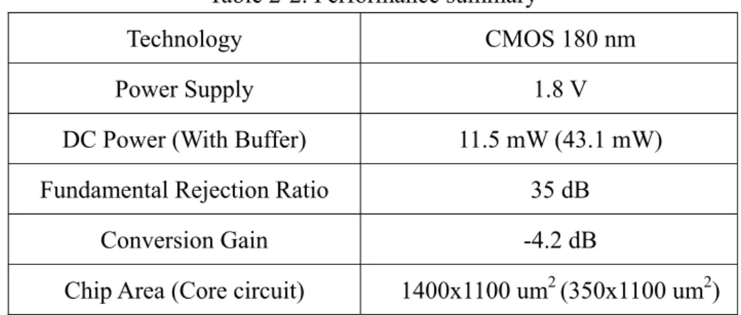
Table 2-2. Performance summary
Technology CMOS 180 nm
Power Supply 1.8 V
DC Power (With Buffer) 11.5 mW (43.1 mW) Fundamental Rejection Ratio 35 dB
Conversion Gain -4.2 dB
Chip Area (Core circuit) 1400x1100 um2 (350x1100 um2)
2.6 Conclusion
A wideband and high linearity balun LNA in 0.18-μm CMOS technology is designed and implemented in this work. With proposed topology, the function of wideband matching and wideband balun has been achieved. From measurement result, the 3-dB band is from 1.27 GHz to 5.31 GHz, and the input return loss is better than 10 dB from 1.74 GHz to 5.2 GHz. This circuit is suitable for wideband communication system application.
The frequency tripler with fundamental cancelling was verified to has 35 dB
HRR1 which is impressive for frequency multiplier circuit design. The power
consumption is another merit compared to other published works. Therefore, this frequency tripler features quadrature signal generation, which is very useful in modern RF transceivers associated with quadrature modulation.
Chapter 3
Circuit Blocks for Direct FSK Demodulator using RFVC
3.1 Introduction
Fig. 3-1 shows the block diagram of proposed direct FSK demodulator using radio-frequency to DC voltage converter (RFVC). The RFVC received the FSK modulated signal from LNA, and converted the frequency information to corresponding output DC voltage. The main difference between traditional FSK demodulator is direct operated in RF signal path. The advantages of proposed demodulator are without extra frequency down-conversion circuit and LO signal source. The design complexity of fully receiver will be simplified. In Section 3-2, the proposed circuit design is described. The chip implement and measurement results are shown in Section 3-3. Finally, a conclusion is given in Section 3-4.
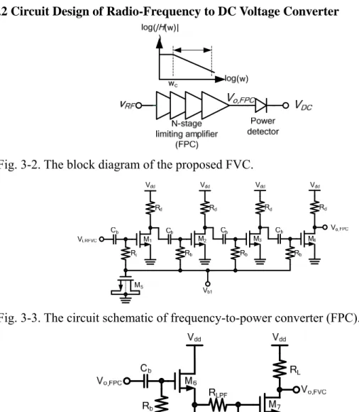
3.2 Circuit Design of Radio-Frequency to DC Voltage Converter
Fig. 3-2. The block diagram of the proposed FVC.
Fig. 3-3. The circuit schematic of frequency-to-power converter (FPC).
Fig. 3-4. The circuit schematic of the power detector.
The circuit block diagram of proposed RFVC is shown in Fig. 3-2. The input signal
vRF is a sinusoidal waveform at the frequency ωo with amplitude of ARF. The dc output
voltage VDC is required to be proportional to ωo, and ideally irrelevant to ARF. The
circuit is composed of two blocks, an N-stage LA for frequency to power converter, and a power detector for power to DC voltage converter.
Essentially the signal frequency can be characterized by utilizing the roll-off response above the pole frequency of a simple-pole circuit. Fig. 3-3 shows a common-source (CS) amplifier for the purpose. It gives a low-pass response with the corner frequency (ωc) determined by the load resistance (Rd) and capacitance at the
output node as L d c C R 1 = ω (3)
signal frequency therefore can be detected from the output power. Nevertheless, ARF
also causes an issue of affecting the output magnitude. To alleviate this issue, the design concept of the limiting amplifier is introduced.
A limiting amplifier is generally used in an optical receiver, where the amplifier operates in the limiting regime such that the output amplitude is constant and insensitive to the input amplitude [7]. This property of amplitude clipping is utilized to minimize the output power variation due to ARF. Different from the conventional
design of a limiting amplifier with bandwidth extension, this design actually makes use of the frequency range above ωc. In this proposed FPC, multiple CS stages are
cascaded to implement the limiting effect. This gives the -3-dB bandwidth (ω-3dB) as
[7] 1 2 3 = ⋅ − −dB ωc N ω , (4)
where N is the number of cascaded stages.
In addition to operating frequency of FVC, the minimum input power level should be considered in this design. Based on the operating mechanism of proposed FVC using LA, increasing voltage gain of LA will achieve this purpose. The voltage gain of LA is shown as below:
d m v g R
A = (5)
Under DC power constrain, increasing Rd is a better choice than gm. Nevertheless,
both the ωc of each amplifier and the operating frequency of FVC will be decreased.
Consequently, the design trade-off is between the operating frequency and minimum input power level.
Four identical CS stages are used as the FPC, each with ωc at 1.66 GHz. Then ω-3dB
is at 0.72 GHz. Each stage is dc-blocked by Cb capacitors. Each transistor is dc biased
at the gate with a resistor Rb of high resistance, except the first stage, where Ri is
selected as 50 ohm for input matching consideration. The transistor M5 gives ac ground from the power supply.
The power detector is composed of a Meyer cell topology and a DC amplifier. The schematics are shown in Fig. 3-4. In Meyer cell design, the transistor M6 received the signal from LA based FPC and converted the magnitude to the corresponding output DC value. A low pass filter which is composed of RLPF and CLPF is placed after power
detector and used to filter the AC feed-through. The more details are described in [7]. The DC amplifier is used for output DC operating range enhancement. The operating current of DC to DC level shifter is controlled by Vo,FPC. The output DC
voltage of proposed RFVC is decided by drain current (Id) and load resistance (RL) of
DC to DC level shifter. The relationship is shown in below:
L d dd FVC o V I R V, = − 7⋅ (6)
3.3 Measurement Results of RFVC
The proposed FVC is designed and fabricated in 0.18 μm CMOS technology. The chip size includes pads for testing is 860 μm x 500 μm. The die photo is shown in Fig. 3-5.
The power dissipation of with input signal at 1 GHz and 5 GHz are 19.4mW and 17.43mW, respectively. Fig. 3-6 shows the output voltage versus input frequency under different input power conditions. With input signal from 1- 5 GHz, the output DC voltage range is from 0.2 V to 1.4 V. Owing to the operating mechanism of LA is introduced in RFPC design, the values of output DC voltage are extremely closely. The output voltage versus input power with different frequencies of input signal is shown in Fig. 3-7. From measurement result, the variation of output DC voltage under same frequency is smaller than 0.046 mV. The performance summary of proposed FVC is shown in Table 3-1.
Fig. 3-5. Die photo.
Fig. 3-6. Input frequency versus output DC voltage.
Fig. 3-7. Input power versus output DC voltage.
Table 3-1. Performance summary and comparison
This work
Technology 0.18 μm CMOS Input frequency range 1-5 GHz Input power dynamic range -7-+5 dBm
Output DC voltage Range 0.215-1.42 V DC power dissipation 17.43-19.4 mW
3.4 Conclusion
A radio-frequency to DC voltage converter (RFVC) is designed and implemented in 0.18 μm CMOS technology. By using proposed mechanism, the input RF signal could be direct- converted to output DC voltage without frequency down- conversion and division. From measurement result, with input signal from 1 GHz to 5 GHz, the output DC voltage is from 0.215 mV to 1.42 mV. And the dynamic range is from -7 dBm to 5 dBm. This work is suitable for RF direct FSK demodulation.
Chapter 4
Wideband Delay Circuit for Time Array System
4.1 Introduction
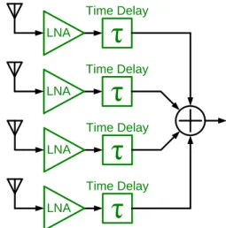
In the modern communication system, the trend will aim to beam-forming system integration. The main methods of implementation are time array and phase array. The most important circuit block of time array system is time delay circuit, and the block diagram is shown in Fig. 4-1. The design goals of this wideband time delay circuit are the extension of operating bandwidth and reduction of circuit area.
This chapter is organized as follows. In Section 4-2, the circuit design is described. The measurement results are summarized in Section 4-3. Finally, a conclusion is given in Section 4-4. LNA Time Delay LNA Time Delay LNA Time Delay LNA Time Delay
4.2 Circuit Design
The ideal time delay circuit essentially exhibits an all-pass filter response with unit gain in the magnitude and a constant group delay over the operation frequency. The transfer function of such a system can be expressed as an exponential functionH(s)=e−std for a group delay of td. A method for implementation is using Padé
approximant [9]. Mathematically, H(s) can be approximately expressed as the first-order and the second-order forms, respectively, as
(7)
The group delay time of the transfer function is defined as the negative differentiation of the phase response. Using (7), the group delay of the 1st-order and 2nd-order APF can be derived, respectively, as
2 0 1 ) ( 1 1 ) ( ω ω ω + = d d t G , (8) 2 0 2 2 0 2 0 2 ) ( ] ) ( 1 [ ) ( 1 ) ( ω ω ω ω ω ω ω Q t Gd d + − + = . (9)
The natural frequency ω0, defined as 1/td, is introduced for convenience. The
group delay remains constant when the operation frequency is smaller than the natural frequency. As the frequency increases, it exhibits dispersion. Fig. 4-2 shows the group delay of the 1st-order and 2nd-order functions (Q=1/√3 for maximum flat delay
bandwidth in the 2nd-order function) for the delay of 50 psec. The higher-order transfer function gives a wider delay bandwidth.
0 2 4 6 8 10 12 10 15 20 25 30 35 40 45 50 G roup delay (p s ) Frequency (GHz) 2nd-order 1 stage 2nd-order 2 stage 1st-order 1 stage 1st-order 2 stage 1st-order 4 stage
Fig. 4-2 Frequency dispersion of the group delay of the transfer functions with different Padé approximants.
Fig. 4-3. The schematic of proposed wideband delay circuit.
The implementation of the 2nd-order transfer function in a single stage is chosen in this work. Fig. 4-3 shows the schematic of the proposed wideband delay circuit. This circuit is composed of a differential pair M1-M2, two common-gate cascode stages
M3-M6 and two common gate amplifiers M7-M8. Actually the circuit implementation is
considered by rewriting the 2nd-order all-pass transfer function in two terms as
2 0 0 2 0 2 2 1 ) ( ω ω ω + + − = s Q s s Q s H . (10)
The first term is unit gain, and the second term represents a transfer function of a band-pass filter. In the proposed circuit, M1 and M2 give a constant gain as the first term,
and the path through M3-M6 yields to the band-pass response. The signals of two paths
are summed up at the drain of M1-M2 in the current domain.
When the summed up current runs through the load, the intrinsic capacitor from the transistors and the loading effect from the next stage give an extra low-pass response to the transfer function. This non-ideal effect will introduce extra group delay and delay dispersion to the entire circuit performance. Even though the inductance peaking technique used in [10] can compensate for delay dispersion, the group delay tends to be sensitive to the resulted overshooting.
In order to alleviate the issue, two common-gate transistors M7-M8 are added as a
buffer stage, rather than as the inductive loading. The output impedance can also introduce inductance peaking by adding resistor Rb on the gate side of M7 and M8.
This inductance peaking introduces a farther zero compare to that in [10], yielding to a larger bandwidth of group delay. The summed current finally goes through M7-M8 to
the load RL, providing unit gain buffering of all-pass response. Rc at the input is for
Limited by the Q value on the band-pass path, the maximum Q value of the entire circuit is 0.5 (in Eq. (3)), which results in the equivalent performance of two cascaded 1st-order delay circuits. The transfer function of the delay circuit can be derived as
2 1 2 2 1 2 2 1 2 1 1 2 2 2 1 2 3 3 1 2 1 1 ) ( 1 1 1 1 ) 1 1 ( Z Z C s C Z C Z s Z Z C s Z C Z C Z Z C R g R g g s R g V V a a a a a m a m m L m i o + + + + ⎥ ⎦ ⎤ ⎢ ⎣ ⎡ − − + − = (11)
where Z1 is the equivalent impedance of Ra parallelto the transconductance of M3., and
Z2 is the source impedance observed from M4 and M6. The product of capacitance and
4.3 Measurement results of Wideband Time Delay Circuit
Fig. 4-4. Die micrograph. The core circuit occupies the area of 320×160 μm2.
Fig. 4-5. The measured S-parameters.
Fig. 4-6. The measured group delay. Fig. 4-7. The measured P1dB versus input
frequency.
The proposed wideband time-delay circuit is designed and fabricated in 0.18 μm CMOS technology. Both input and output ports are differential. Fig. 4-4 shows the die micrograph. The core circuit occupies the area of 320×160μm2. The total chip size is
520×820 μm2. The DC power consumption of core circuit and buffer are 7.88 mW
and 8.91 mW from 1.8 V power supply, respectively.
The measurement result of S-parameter is shown in Fig. 4-5. The input and output matching return loss are better than 10 dB up to 10 GHz. The loss of proposed time-delay circuit at 1 GHz and 5 GHz are 5.72 dB and 8.93 dB, respectively. Due to the output buffer of a source follower, the gain level of the entire circuit becomes less than 0 dB. This can be recovered in a fully integrated circuit design. Fig. 4-6 shows the measured group delay. At low frequencies, it appears to be flat around 45 psec. The group delay becomes 37.2 psec at 5 GHz. The linearity performance of the measured P1dB versus input frequency is shown in Fig. 3-7. The worst P1dB is -4.72
dBm at 1 GHz. Since the gain level drops as frequency increases, P1dB increases to be
4-4 Conclusions
A wideband 2nd-order delay circuit in 0.18-μm CMOS technology is presented with
the features of double delay bandwidth of the 1st-order active all-pass filter. The main principle is to use Padé approximant for all-pass filter design, which has an advantage of smaller chip area from passive delay line.
Chapter 5
High Input Power Range Phase Shifter for Transmitter Array
Application
Fig. 5-1. Block diagram of RF-path shifter transmitter array
5.1 Introduction
The other method for beam-forming implementation is phase array system, and the key component is the phase shifter. The block diagram of RF-path shifting phase array transmitter is shown in Fig. 5-1.
In phase shifter design, the technique of I/Q vector combination is widely used in the active scheme. The desired output signal phase can be synthesized by summing a pair of quadrature I and Q input signals, each with an appropriate magnitude. By using two of the four input phases of 0o, 90o, 180o, and 270o, a full range of
360-degree output phase can be achieved. The scheme therefore requires variable gain amplifiers (VGAs) to adjust the magnitude of the I/Q signals to the desired ratio.
The design issue arises from VGA linearity. Although the phase shifting resolution is loose, the shifted phase shall remain constant irrelevant to the signal content. Consider the complicated modulation technique in modern digital communications normally with high signal peak-to-average ratio (PAR). If the VGA causes nonlinear amplitude distortion, the output phase of the shifter varies along with the modulated signal envelope. The output signal then suffers from the error vector magnitude (EVM) degradation, similar to the AM-to-PM distortion issue in power amplifier design.
The typical implementation of VGA calls for the conFiguration of a differential amplifier, which voltage gain is controlled by the device transconductance, or, in turn, the bias current [11], [12]. Given a bias current setting, the transconductance only remains constant within a limited range of the input signal swing. Since the modulated signal envelope variation could be more than 10 dB, it is critical to permit a large
dynamic range of the input signal swing for a given phase shift. This issue is seldom discussed for phase shifter implementation. For example, if the average phase distortion to signal data symbols were 2°, the phase shifter would cause EVM of -29.14 dB. This degradation would fail conformance requirements in modern communication systems, such as WiMAX.
In this circuit, a phase shifter using modified VGA design is proposed to overcome this issue. The revised schematic improves the linearity of the I/Q vector combiner. Thus, it improves the accuracy of phase shift.
This chapter is organized as follows. In Section 5.2, the proposed circuit design is described. The chip implement and measurement results are shown in Section 5.3. Finally, a conclusion is given in Section 5.4.
5.2 Circuit Design
The commonly used VGA design in a phase shifter with I/Q vector combination technique is as shown in Fig. 5-2 [11], [12]. Signal appears in the differential format. The phase shifter consists of four differential amplifiers in a group of two. Each group amplifies the I or Q signal to the specified output level. Essentially the two input signals in each group are simply phase inversed to each other, yielding to summation or subtraction. Only one signal in each group is amplified and summed up at the output in the current domain. Gain control and input signal selection are realized by tuning the dc bias current to the specified transconductance. By doing so, the output phase covers the full range of 360 degrees.
Fig. 5-2 Block diagram of a conventional I/Q vector combiner phase shifter.
Fig. 5-3 Phase distortion versus input swing of commonly used VGA
The issues of the VGA circuit configuration are twofold. One is the transconductance variation along with the input signal swing. If the input swing becomes large, device nonlinearity causes the effective dc bias to change. Thus the amplifier gain changes correspondingly. The other is the gain variation due to gain tuning in another amplifier pair. In deep submicron devices, the device transconductance varies notably at different VDS bias even if the bias current is fixed.
In this conFiguration, the dc voltage of Vop and Von actually changes if the bias
current changes in one transistor pair. The gain level of a transistor pair therefore is affected by gain tuning in another pair.
selected DC current is not suitable for wide dynamic input swing. For example, if we choose different bias condition for each gain state of I/Q path under small signal operation, the phase distortion and gain variation of output signal will be extremely low. But these bias conditions are not suitable for large signal operation owing to VGA linearity issue. Nevertheless, the phase shifter on the RF path shall handle both small signal and large signal swings of the modulated signal without phase distortion. Fig. 5-3 shows the simulated phase distortion of commonly used VGAs. Owing to the linearity of I/Q ac magnitude ratio, if the desired output phase is at 22.5° and 67.5°, the phase distortion will increase to 10 degrees when the input swing is 300 mV.
Fig. 5-4 Schematic of proposed VGA and vector combiner
Fig.5-5 Diagram of phase shift base on I/Q vector combiner
5.2.1 Proposed Variable Gain Amplifier
To solve the phase distortion issue, the VGA circuit is proposed for phase shifter design, as shown in Fig. 4. The circuit takes four-phase input signals. The difference from the traditional phase shifter is gain control, which is implemented by four sets of differential amplifier cells. Each cell is biased with a current source that is digitally controlled by switching ON/OFF. Each set includes gain cells in different device sizes, resulting in weighted output currents for vector combination at the nodes Vop and Von.
transconductance is also fixed, namely, irrelevant to the input voltage swing.
The output phase resolution relies on the gain control to I and Q signals, and in turn on the device size ratio among gain cells.
This concept is similar to the programmable gain amplifier (PGA) in [13]. Fig. 5-5 shows the magnitude ratio of I/Q signals to synthesize the phase resolution of 22.5° with equal magnitudes. Calculated by arctangent function, the integral I/Q ratio of 0°, 22.5°, 45°, 67.5°, and 90° are 13/0, 12/5, 9/9, 5/12, and 0/13, respectively. The device sizes in a set of gain cells need to be chosen properly. Although binary weighting allows high resolution [6], the sizes of x1, x3, x4, x5 are chosen in this work for minimum hardware implementation. The congenital theoretical phase error and gain variation are 0.12° and 0.092 dB, respectively.
By using proposed schematic of VGA in I/Q vectors combination based phase shifter design, the mechanism of gain tuning only depends on the accuracy of device ratio. The bias condition of each gain cell is fixed in ON state. This is the maximum difference between commonly used VGA and proposed VGA. Based on proposed VGA, the sensitivity of VDS could be reduced. The phase distortion and gain variation
of phase shifter will be improved in wide input power range.
5.2.2 Quadrature Phase Generator and Output Buffers
The phase shifter requires quadrature phase input signals. In this design, an RC poly-phase filter (PPF) is adopted to convert a differential input for the purpose. A 100-Ω resistor is also placed in shunt to the input for impedance matching. As such, the PPF introduces significant signal loss. The simulated result shows that the voltage loss of the PPF is 5.75 dB at 3.5 GHz. This voltage loss is subtracted from measurement data in phase shifter gain calculations.
At the phase shifter output, a source follower stage is included as an output buffer for impedance matching for measurement. The voltage loss of the output buffer is 7.5 dB at 3.5 GHz.
5.3 Circuit Implement and Measurement Results
The proposed phase shifter was fabricated using 0.18-μm standard CMOS technology. Fig. 5-6 shows the die photo of this work. The core circuit which includes an RC PPF, VGA and output buffers occupies 793 μm x 280 μm chip area. The total chip size, including testing pads, is 1015 μm x 805 μm.
Fig. 5-7 shows the phase shift versus input power of 16 different phase states at 3.5 GHz. The phase shifter gain at 3.5 GHz is shown in Fig. 5-8. The averaged gain of the proposed phase shifter, including VGA, and output buffer, is about -12.47 dB. The measured phase distortion versus input power is shown in Fig. 5-9. In this work, by using the proposed VGA, the gain variation is below 1.5 dB and phase distortion is small than ±2°. The frequency responses of the phase shift and gain are shown in Fig. 5-10 and Fig. 5-11. The values of the phase error and gain variation increase with the frequency offset to the corner frequency of PPF. The maximum phase error and gain variation are 5° and 2 dB in the operating frequency band from 3 GHz to 4 GHz.
Owing to the operated mechanism of proposed VGA, the DC dissipations of 16 phase states are not equally. With 1.8 V supply voltage, the maximum the minimum power dissipation are 21.27 mW and 15.46 mW, respectively. The output buffers consumes 15.62 mW from 1.8 V supply. The power consumption depended on the transconductance of active device, if the advance technology could be used in this design, the power consumption could be reduced. The performance summary and comparison is shown in Table 1.
Fig. 5-6 Chip photo Fig. 5-7 Phase shift versus input power
Fig. 5-8 Gain versus input power Fig. 5-9 Phase distortion versus input power
Fig. 5-10 Phase shift versus input frequency
5.4 Conclusion
A 3.5 GHz high dynamic input power range phase shifter in 0.18-μm CMOS technology is designed and implemented in this work. With proposed schematic of VGA, the dynamic of input power of gain variation and phase error could be improved. From measurement results, when the input power range was swept from -33 dBm to 7 dBm, the phase distortion and gain variation versus input power of proposed phase shifter are smaller than ±2° and 1.5 dB, respectively. This circuit is suitable for wide dynamic input power range and high accuracy of phase and gain application.
Chapter 6 Conclusions and Future Works
6.1 Conclusions
In this report, the circuit blocks for wideband frequency operation and beam-forming system are designed and implemented. From the measurement result, the design targets have been achieved.
A 1.27-5.31 GHz wideband, high linearity balun LNA is suitable for the first stage design in receiver chain, and the 3-5.7 GHz frequency tripler is also suitable for wideband LO source generator.
Otherwise, for FSK demodulation requirement, a direct radio-frequency to DC voltage converter is developed and implemented. The wideband LO signal source is not necessary demand in this FSK demodulator, so the design complexity, and chip size will has a significant reduction.
For beam-forming system design, the 3 dB bandwidth of proposed wideband delay circuit is extended to 4.38 GHz without any inductor peaking which will reduce silicon area. This circuit has a great potential for fully time array system integration. In phase shifter design, the wide input dynamic range requirement is solved by proposed method. This circuit is also suitable to phase array transmitter integration. These works are also presented in Mater Theses [14], [15] of National Chiao-Tung University.
6.2 Future Work
The design techniques of most critical circuit blocks for wide frequency band operation and beam-forming system have been developed. The further progress is the integration of fully system.
For Chapter 2, the down conversion mixer, IF amplifier and a frequency synthesizer could be integrated with proposed LNA and frequency tripler. And then, the wideband receiver will be implemented.
For Chapter 3, the wideband LNA which is developed in Chapter 2 could be reused an integrated with proposed RFVC. The direct FSK demodulator could be demonstrated.
Finally, for future communication systems, the most important circuits which are time delay circuit and phase shifter should be integrated in beam-forming receiver and transmitters.
Reference
[1] Andrea Bevilacqua, and Ali M. Niknejad, “An Ultrawideband CMOS Low-Noise Amplifier for 3.1–10.6-GHz Wireless Receivers,” IEEE Journal of Solid-State
Circuits, vol. 39, no. 12, pp.2259-2268, December 2004.
[2] Ming-Ching Kuo, Chien-Nan Kuo, and Tzu-Chan Chueh, “Wideband LNA Compatible for Differential and Single-Ended Inputs,” IEEE Microwave and Wireless
Components Letters, vol. 19, no. 7, pp. 482-484, July 2009.
[3] Ming-Ching Kuo, Shiau-Wen Kao, Chih-Hung Chen, Tsung-Shuen Hung, Yi-Shing Shih, Tzu-Yi Yang, and Chien-Nan Kuo, ”A 1.2 V 114 mW Dual-Band Direct-Conversion DVB-H Tuner in 0.13 μm CMOS,” IEEE Journal of Solid-State Circuits, vol. 44, no. 3, pp. 740-750, March 2009.
[4] Chih-Fan Liao, and Shen-Iuan Liu, “A Broadband Noise-Cancelling CMOS LNA for 3.1-10.6-GHz UWB Receivers,” IEEE Journal of Solid-State Circuits, vol. 42, no. 2, pp. 329-339, February 2007.
[5] Ali Meaamar, Boon Chirn Chye, Do Man Anh, and Yeo Kiat Seng, “A 3-8 GHz Low-Noise CMOS Amplifier,” IEEE Microwave and Wireless Components Letters, vol. 19, no. 4, pp. 245-247, April 2009.
[6] Stephan C. Blaakmeer, Eric A. M. Klumperink, Domine M. W. Leenaerts, and Bram Nauta, “A Wideband Noise-Canceling CMOS LNA Exploiting A Tramsformer, ” IEEE Radio Frequency Integrated Circuits Symposium, 2006.
[7] B. Razavi, Design of Integrated Circuits for Optical Communications, McGraw-Hill Chapter 5, pp. 125- 127, 2003.
[8] H. T. Bui, and Y. Savaria, “Design of a High-Speed Differential Frequency-to-Voltage Converter and Its Application in a 5-GHz Frequency-Locked Loop,” IEEE Trans. on Circuits and Systems- I, vol. 55, no. 3, pp. 766- 774, April 2008.
[9] Baker, Jr., G.A., and Graves-Morris, P.: Padé approximants. (Cambridge University Press, New York, 1996)
[10] Moonkyun Maeng, Franklin Bien, Youngsik Hur, et al., “0.18- m CMOS Equalization Techniques for 10-Gb/s Fiber Optical Communication Links,” IEEE
Transactions on Microwave Theory and Techniques, vol. 53, no. 11, pp. 3509-3519,
Nov. 2005.
[11] Kwang-Jin Koh and Gabriel M. Rebeiz, “0.13- m CMOS Phase Shifters for X-, Ku-, and K-Band Phased Arrays,” IEEE Journal of Solid-State Circuits, vol. 42, no. 11, pp. 2535-2546, Nov. 2007.
[12] Karen Scheir, Stephane Bronckers, Jonathan Borremans, Piet Wambacq, and Yves Rolain, “A 52 GHz Phased-Array Receiver Front-End in 90 nm Digital CMOS,”
IEEE Journal of Solid-State Circuits, vol. 43, no. 12, pp. 2651-2659, Dec. 2008.
[13] Hsin-Hung Kuo, Yang-Han Li, and Yi-Hsin Pang, ”A 0.13- m CMOS Transmitter with 72-dB RF Gain Control for Mobile WiMAX/WiBro Applications,”
IEEE Radio Frequency Integrated Circuits Symposium, 2008, pp.105-108.
[14] 蔡建忠, “應用於射頻發送端之低功率電路," 碩士論文,國立交通大學, 2010 年
Self-Evaluation
3. 請依學術成就、技術創新、社會影響等方面,評估研究成果之學術或應用價 值(簡要敘述成果所代表之意義、價值、影響或進一步發展之可能性) 本子計畫研究成果為應用於寬頻通訊接收機系統中的關鍵電路技術,包含一 個具有單端-雙端轉換功能的寬頻低雜訊放大器、提供 3GHz-5.7GHz 的本地振 盪源頻率輸出的三倍頻器、寬頻延遲電路、3-4 GHz 具有高輸入動態範圍的 相移器、1-5 GHz 頻率-電壓轉換器。分別敘述如下: (1)具有單端-雙端轉換功能的寬頻低雜訊放大器 本電路主要貢獻在於將傳統需要分成兩級設計的低雜訊放大器與單端-雙端轉換 器,利用電路技巧結合成一個電路,降低電路元件數目與晶片面積。此外,本電 路提出可以改善增益與線性度的技術,但是沒有消耗額外的直流功率,使本電路 更適合用於系統整合中。進一步發展為整合下一級的混頻器與中頻可調增益放大 器,進而完成整個接收機系統。 (2) 提供 3-5.7 GHz 的本地振盪源頻率輸出的三倍頻器 本電路的主要貢獻為提出新式三倍頻產生器與一個可以消除輸出一倍頻的電路 技巧。有別於傳統利用被動濾波器的方式,本電路使用向量相消的方式,可大幅 降低核心的晶片面積,有助於系統整合的應用。進一步發展為整合頻率合成器, 如此一來可實現 1-1.9 GHz 與 3-5.7 GHz 雙頻帶的本地振盪源系統。 (3)1-5 GHz 頻率-電壓轉換器 本電路的貢獻為實現一個操作在 GHz 頻段的頻率電壓轉換器。主要貢獻為將傳統 只能操作在幾百 MHz 的電路方塊,利用不同的電路技術,大幅提升電路操作頻 率。此電路的優勢為不需要做頻率降頻的動作,可以直接偵測在 GHz 頻段的射頻 信號,降低電路設計的複雜度。進一步發展為整合前端放大器,可以製作成 FSK 解調器。另一個發展為與 PLL 作整合,可以增快鎖定的時間。 (4) 寬頻延遲電路 本電路實現一個操作頻率從 DC-4.38 GHz 的寬頻延遲電路,主要貢獻為使用主動 二階電路取代傳統利用電感來延伸頻寬的方式,本電路的優勢為縮小電路面積。 進一步發展為運用於時間陣列系統的整合以及基頻的等化器設計中。 (5) 3-4 GHz 具有高輸入動態範圍的相移器 本電路的貢獻為針對發射機因調變訊號振幅變化對傳統相移器會產生額外相位 與振幅失真做改善。本電路在相移器採用數位式的可調增益放大器來調整輸出的 相位,此電路優勢為增加電路的輸入動態範圍,適合用於發射機的整合。進一步 發展為與功率放大器、升頻器做完整的波束成型(beam-forming)系統。出席國際學術會議心得報告
會議名稱: 2010 IEEE Asian Solid-States Circuit Conference (A-SSCC) 會議時間: Nov. 8~10, 2010 報告人:郭建男/國立交通大學電子工程系/副教授 一、參加會議經過 ASSCC會議屬於亞洲在IEEE固態電路領域一個主要會議,特色在於討論積體電路設計技 術。今年由中國清華大學主辦,舉辦地點位於北京市在奧運會場附近的五洲旅館。本會 議輪流由台灣,日本,韓國及大陸舉辦,從2005年在台灣開始,已經是第二輪。根據以 往統計,只要在中國舉辦,參加人數都顯得較少,今年可能約略少於300人參與,但台灣 參與的人員不少。 議程日期共包含有三天,但IEEE固態電路之會議一項重視口頭報告品質,所有報告之作 者必須提前一天(11月7日)抵達,和議程主席與副主席共同預演,並進行內容調整與修改。 此外,本會議還有一特色,為學生論文競賽,作者被要求必須現場提供實物展示與操作, 由評審委員觀察、發問與討論,然後在大會稍候進行頒獎。今年本校有研究團隊提出高 效能無線傳送機應用之基頻數位電路設計,不僅進入決賽,更在十餘隊伍中獲得優勝。 大會之第一天為workshop及tutorial課程,提供與會人士選擇學習。議程於接下來二天中 進行,口頭報告部份有15個議程,二個上午大會共安排四個邀請演講,今年由工研院資 通所吳成文所長開始第一場,報告3D IC之主題,之後為日本NHK公司伊騰博士報告有關 3D電視相關主題,瞭解未來電視可以跳脫平面式,呈現給人類3維視覺效果,的確有趣。 二、與會心得 此會議延續從前在亞太區的AP-ASIC國際會議,在2005年開始由IEEE支持舉辦,對固態積 體電路設計技術討論。論文要被接受,得提出晶片實作與測試結果,標準一向很高,接 受率一直約在30~40%,投稿內容已經甚少出現只有模擬結果。幾年下來,可以觀察出國 際社會在此領域有新成員加入,例如新加坡這幾年不僅積極投稿,也爭取在2013年主辦 機會。而大陸在這幾年的設計技術成長,著實明顯讓人看得出來,而且對系統規劃與設 計的能力,已經可以跨入與其他國家競爭行列。台灣的能力雖仍然有強勢之處,但已經 不多,隨時可能被超越,務必警惕在心。今年在本人研究領域相關之射頻電路設計方面, 在毫米波相關部份已經出現涵蓋超過100GHz之放大器設計,值得注意。 三、攜回資料名稱及內容 會議論文資料。國科會補助計畫衍生研發成果推廣資料表
日期:2011/10/31國科會補助計畫
計畫名稱: 子計畫二:可重組式 Mixed-signal/MEMS .9G~10GHz射頻接收端設計(2/2) 計畫主持人: 郭建男 計畫編號: 99-2220-E-009-041- 學門領域: 晶片科技計畫--整合型學術研究 計畫無研發成果推廣資料
99 年度專題研究計畫研究成果彙整表
計畫主持人:郭建男 計畫編號: 99-2220-E-009-041-計畫名稱:異質整合 Mixed-signal/MEMS CMOS 無線射頻收發機設計研發--子計畫二:可重組式 Mixed-signal/MEMS .9G~10GHz 射頻接收端設計(2/2) 量化 成果項目 實際已達成 數(被接受 或已發表) 預期總達成 數(含實際已 達成數) 本計畫實 際貢獻百 分比 單位 備 註 ( 質 化 說 明:如 數 個 計 畫 共 同 成 果、成 果 列 為 該 期 刊 之 封 面 故 事 ... 等) 期刊論文 0 0 100% 研究報告/技術報告 0 0 100% 研討會論文 0 0 100% 篇 論文著作 專書 0 0 100% 申請中件數 0 0 100% 專利 已獲得件數 0 0 100% 件 件數 0 0 100% 件 技術移轉 權利金 0 0 100% 千元 碩士生 0 0 100% 博士生 0 0 100% 博士後研究員 0 0 100% 國內 參與計畫人力 (本國籍) 專任助理 0 0 100% 人次 期刊論文 0 0 100% 研究報告/技術報告 0 0 100% 研討會論文 3 0 100% 篇 論文著作 專書 0 0 100% 章/本 申請中件數 0 0 100% 專利 已獲得件數 0 0 100% 件 件數 0 0 100% 件 技術移轉 權利金 0 0 100% 千元 碩士生 0 0 100% 博士生 0 0 100% 博士後研究員 0 0 100% 國外 參與計畫人力 (外國籍) 專任助理 0 0 100% 人次其他成果