IEEE ELECTRON DEVICE LETTERS, VOL. 34, NO. 5, MAY 2013 617
Hopping Effect of Hydrogen-Doped Silicon Oxide
Insert RRAM by Supercritical CO
2
Fluid Treatment
Kuan-Chang Chang, Chih-Hung Pan, Ting-Chang Chang, Senior Member, IEEE, Tsung-Ming Tsai, Rui Zhang,
Jen-Chung Lou, Tai-Fa Young, Jung-Hui Chen, Chih-Cheng Shih, Tian-Jian Chu, Jian-Yu Chen, Yu-Ting Su,
Jhao-Ping Jiang, Kai-Huang Chen, Hui-Chun Huang, Yong-En Syu, Der-Shin Gan, and
Simon M. Sze, Life Fellow, IEEE
Abstract— In this letter, we introduced hydrogen ions into titanium metal doped into SiO2 thin film as the insulator of
resistive random access memory (RRAM) by supercritical carbon dioxide (SCCO)2fluid treatment. After treatment, low resistance
state split in to two states, we find the insert RRAM, which means it has an operating polarity opposite from normal RRAM. The difference of the insert RRAM is owing to the resistive switching dominated by hydrogen ions, dissociated from OH bond, which was not by oxygen ions as usual. The current conduction mechanism of insert RRAM was hopping conduction due to the metal titanium reduction reaction through SCCO2.
Index Terms— Hopping conduction, resistive random access memory (RRAM), supercritical fluid.
I. INTRODUCTION
R
ECENTLY, next-generation memories have been widely investigated. Resistance random access memory (RRAM) is one of the most popular memory devices, due to its simple structure, high-switching speed, low-operation power, and nonvolatile characteristic [1]–[8]. Besides, silicon-based oxide is a promising material for RRAM application owing to its great compatibility in IC processes. Thus, the silicon-base oxide was selected as the resistance-switching layer in our research. The supercritical carbon dioxide (SCCO2) fluidManuscript received January 3, 2013; accepted March 5, 2013. Date of publication April 3, 2013; date of current version April 22, 2013. This work was supported in part by the National Science Council Core Facilities Lab-oratory for Nano-Science and Nano-Technology in the Kaohsiung-Pingtung area and the National Science Council of China, under Contract NSC-101-2120-M-110-002 and Contract NSC 101-2221-E-110-044-MY3. The review of this letter was arranged by Editor T. San.
K.-C. Chang, C.-H. Pan, T.-M. Tsai, T.-J. Chu, J.-P. Jiang, H.-C. Huang, and D.-S. Gan are with the Department of Materials and Optoelectronic Science, National Sun Yat-Sen University, Kaohsiung 80424, Taiwan.
T.-C. Chang, J.-Y. Chen, Y.-T. Su, and Y.-E. Syu are with the Department of Physics, National Sun Yat-Sen University, Kaohsiung 80424, Taiwan, and also with the Advanced Optoelectronics Technology Center, National Cheng Kung University, Tainan 70101, Taiwan (e-mail: [email protected]). R. Zhang and J.-C. Lou are with the School of Software and Microelec-tronics, Peking University, Beijing 100871, China
T.-F. Young is with the Department of Mechanical and Electro-Mechanical Engineering, National Sun Yat-Sen University, Kaohsiung 80424, Taiwan.
J.-H. Chen and C.-C. Shih are with the Department of Chemistry, National Kaohsiung Normal University, Kaohsiung 802, Taiwan.
K.-H. Chen is with Department of Electronics, Tung Fang Institute of Technology, Kaohsiung 829, Taiwan.
S. M. Sze is with the Department of Electronics Engineering, National Chiao Tung University, Hsinchu 300, Taiwan.
Color versions of one or more of the figures in this letter are available online at http://ieeexplore.ieee.org.
Digital Object Identifier 10.1109/LED.2013.2251995
(c)
(a) (b)
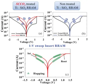
Fig. 1. (a) Current–voltage curve of the resistive switching characteristic of Ti:SiO2 device with SCCO2 treatment. (b) Current–voltage curve of the
resistive switching characteristic of Ti:SiO2device without SCCO2treatment.
(c) Current conduction curve of the insert RRAM. The conduction mechanism is the hopping conduction both at HRS and LRS.
mixed with pure water as co-solvent treating thin film has been regarded as an efficient way to transport H2O molecules
into the microstructure of the switching layer to improve dielectric properties, because of its high penetration and liquid-like characteristics [9]–[11]. In this research, titanium metal doped into SiO2 (Ti:SiO2) by co-sputtering at room
temperature was taken as the resistance switching layer of RRAM. The conduction mechanism and material analyses were discussed to explain the phenomenon of insert RRAM occurred after SCCO2 fluid treatment.
II. EXPERIMENTALSETUP
First, the Ti:SiO2thin film (about 10 nm) was deposited on
the TiN/Ti/SiO2/Si substrate by co-sputtering with the pure
SiO2 and titanium targets. After that, the Ti:SiO2 thin films
were put into the chamber of supercritical fluid system at 120 °C for 1 h, the chamber was injected with SCCO2 fluid
at the pressure of 3,000 psi which were mixed with 5 vol%
618 IEEE ELECTRON DEVICE LETTERS, VOL. 34, NO. 5, MAY 2013
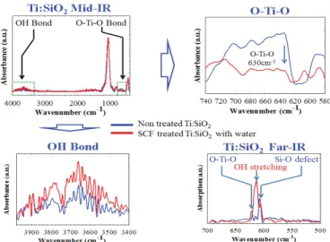
Fig. 2. FTIR spectrums of Ti:SiO2film with and without SCCO2treatment.
The signal of O–H and O–H stretching bond increased, and the O–Ti–O bond decreased after SCCO2treatment.
Fig. 3. XPS spectra of Ti 2p3/2 and Si 2p3/2 core level in Ti:SiO2 film
before and after SCCO2treatment. By quantum analysis, The mole fraction
of O–Ti–O bonds in Ti:SiO2film is reduced obviously but that of O–Si–O
bonds are increased after SCCO2 treatment.
pure H2O. Finally, the Pt top electrode of 200 nm thickness
was deposited on Ti:SiO2 film to form the RRAM devices
with Pt/Ti:SiO2/TiN structure. The electrical analyses of all
devices were performed using Agilent B1500 semiconductor parameter analyzer.
III. RESULTS ANDDISCUSSION
In order to understand the influence of SCCO2-treated
Ti:SiO2 RRAM device, the device was measured for
elec-trical analyses before and after SCCO2 fluid treatment. The
insert RRAM appeared after the SCCO2 treatment shown as
Fig. 1(a), which is opposite to normal RRAM in operating polarity. In the insert RRAM, the set process was com-pleted in the negative bias sweep cycle. In contrast, the reset process was accomplished in the positive bias sweep cycle. However, the insert RRAM was not found in the Ti:SiO2
RRAM device before SCCO2 treatment shown as Fig. 1(b).
Fig. 4. Diagram of the resistive switching of the insert RRAM, and the energy band of carrier hopping effect in the resistance-switching layer.
The HRS of insert RRAM and the low resistance state (LRS) of normal RRAM have same state. In order to present the insert RRAM, we have to control the stop voltage precisely so as to get sweep cycles to analyze its characteristics. Besides, the current conduction mechanism was dominated by hopping conduction both in HRS and LRS of the insert RRAM shown as Fig. 1(c). And the hopping conduction equation is J = q Naυ0e−qφT/kTeqaV/2dkT, where N , a,
φT, υ0, and d are density of space charge, mean of
hop-ping distance, barrier height of hophop-ping, intrinsic vibration frequency, and film thickness, respectively. To investigate the interesting phenomena on resistive switching of insert RRAM, the Fourier transform infrared spectroscopy (FTIR) was conducted to do material analyses. In the Fig. 2, the signal of O–Ti–O bond at 630 cm−1 was decayed after SCCO2fluid
treatment, and the signal of OH bond at 3400–3600 cm−1 was increased. Meanwhile, the signal of O–H stretching bond at 636 cm−1 was also increased after SCCO2 fluid treatment
[12], which can be observed in Far-IR region of FTIR. According to Beer’s law, the absorption coefficient and the thickness of the film did not change during the SCCO2 fluid
treatment, the intensity of signal is proportional to the con-centration of the corresponding bond. Therefore, the TiO2was
deoxidized to Ti element and Si was oxidized in the Ti:SiO2
film after SCCO2 fluid treatment. Besides, the OH bond was
brought into the film through treatment. Then, the material analyses were used to verify the change of oxidation number of Ti and Si by X-ray photoelectron spectroscopy (XPS) shown in Fig. 3. Before SCCO2fluid treatment, there was 43% of TiO2
and 57% of Ti2O3in the titanium oxide of Ti:SiO2film, but no
metal titanium exist in the film. Based on the deconvolution of Si 2P3/2 core level, a few Si bonding signal was found
in Ti:SiO2 film. After the SCCO2 treatment, the titanium
oxide of Ti:SiO2 film was deoxidized and changed into metal
titanium while silicon of Ti:SiO2film was oxidized into silicon
oxide. According to material analyses, we found OH bond increased and some oxidation–reduction reactions happened in Ti:SiO2film during SCCO2fluid treatment. So, we proposed a
CHANG et al.: HOPPING EFFECT OF HYDROGEN-DOPED SILICON OXIDE INSERT RRAM 619
shown in Fig. 4. The nucleus of metal titanium caused the defect of the film, leading to the hopping conduction at HRS of insert RRAM. Owing to the increasing of OH bond, the hydrogen ions generated from OH bond broken were attracted to TiN electrode when supplied a negative bias, resulting in Si–O bond broke during the hydrogen ions migration. The silicon dangling bond also increased the density of defect to reduce the hopping distance, leading to the increase of current in SCCO2-treated device. This would make the set process
occur at a negative bias. On the contrary, the reset process of insert RRAM would occur at positive bias due to the opposite migration of hydrogen ions.
IV. CONCLUSION
In conclusion, the insert RRAM which is opposite to normal RRAM in operating polarity was observed in the Ti:SiO2
device after SCCO2 fluid treatment. According to material
analyses of XPS and FTIR, we found the Ti:SiO2 film could
increase OH bond through SCCO2 treatment. The OH bond
provided plenty of hydrogen ions during negative bias, leading to set process. The dangling bond from nucleus of metal titanium and Si–O broken bond supplied more defect to resulting carrier hopping conduction by means of the hydrogen ions migration. These phenomena will result in insert RRAM for SCCO2-treated Ti:SiO2RRAM.
REFERENCES
[1] Y. E. Syu, T. C. Chang, T. M. Tsai, Y. C. Hung, K. C. Chang, M. J. Tsai, M. J. Kao, and S. M. Sze, “Redox reaction switching mechanism in RRAM device with Pt/CoSiOX/TiN structure,” IEEE Electron Device
Lett., vol. 32, no. 4, pp. 545–547, Apr. 2011.
[2] K. C. Chang, T. M. Tsai, T. C. Chang, Y. E. Syu, S. L. Chuang, C. H. Li, D. S. Gan, and S. M. Sze, “The effect of silicon oxide based RRAM with tin doping,” Electrochem. Solid-State Lett., vol. 15, no. 3, pp. H65–H68, 2012.
[3] T. M. Tsai, K. C. Chang, H. C. Huang, and D. S. Gan, “Bipolar resistive RAM characteristics induced by nickel incorporated into silicon oxide dielectrics for IC applications,”
IEEE Electron Device Lett., vol. 33, no. 12, pp. 1696–1698,
Dec. 2012.
[4] Q. Liu, S. B. Long, W. Wang, Q. Y. Zuo, S. Zhang, J. N. Chen, and M. Liu, “Improvement of resistive switching properties in ZrO2
-based ReRAM with implanted Ti ions,” IEEE Electron Device Lett., vol. 30, no. 12, pp. 1335–1337, Dec. 2009.
[5] Y. Wang, Q. Liu, S. B. Long, W. Wang, Q. Wang, M. H. Zhang, S. Zhang, Y. T. Li, Q. Y. Zuo, J. H. Yang, and M. Liu, “Investigation of resistive switching in Cu-doped HfO2 thin film
for multilevel non-volatile memory applications,” Nanotechnology, vol. 21, no. 4, p. 045202, 2010.
[6] Y. T. Li, S. B. Long, M. H. Zhang, Q. Liu, L. B. Shao, S. Zhang, Y. Wang, Q. Y. Zuo, and S. Liu, and M. Liu, “Resistive switching properties of Au/ZrO2/Ag structure for low voltage nonvolatile memory
applications,” IEEE Electron Device Lett., vol. 31, no. 2, pp. 117–119, Feb. 2010.
[7] Q. Liu, C. Dou, Y. Wang, S. Long, W. Wang, M. Liu, M. Zhang, and J. Chen, “Formation of multiple conductive filaments in the Cu/ZrO2:Cu/Pt device,” Appl. Phys. Lett., vol. 95, no. 2,
pp. 023501-1–023501-3, 2009.
[8] Q. Liu, S. Long, H. Lv, W. Wang, J. Niu, Z. Huo, J. Chen, and M. Liu, “Controllable growth of nanoscale conductive fila-ments in solid-electrolyte-based ReRAM by using metal nanocrystal cover bottom electrode,” ACS Nano, vol. 4, no. 10, pp. 6162–6168, 2010.
[9] K. C. Chang, T. M. Tsai, T. C. Chang, and Y. E. Syu, “Reducing opera-tion current of Ni-doped silicon oxide resistance random access memory by supercritical CO2fluid treatment,” Appl. Phys. Lett., vol. 99, no. 26,
pp. 263501-1–263501-4, 2011.
[10] T. M. Tsai, K. C. Chang, T. C. Chang, and Y. E. Syu, “Dehydroxyl effect of Sn-doped silicon oxide resistance random access memory with supercritical CO2fluid treatment,” Appl. Phys. Lett., vol. 101, no. 11,
pp. 112906-1–112906-4, 2011.
[11] T. M. Tsai, K. C. Chang, K. H. Liao, and H. C. Huang, “Origin of hopping conduction in Sn-doped silicon oxide RRAM with supercritical CO2 fluid treatment,” IEEE Electron Device Lett., vol. 33, no. 12,
pp. 1693–1695, Dec. 2012.
[12] R. K. Singh and A. Srinivasan, “Bioactivity of ferrimagnetic MgO–CaO–SiO2–P2O5-Fe2O3 glass-ceramics,” Ceram. Int., vol. 36,