國
立
交
通
大
學
電子物理研究所
博 士 論 文
高品質氧化鋅、氧化鎂鋅、氧化錳鋅與氧化鎘鋅
之成長與光學研究
Growth and optical study of high quality
ZnO, ZnMgO, ZnMnO and ZnCdO
研 究 生:簡崑峯
指導教授:周武清 教授
高品質氧化鋅、氧化鎂鋅、氧化錳鋅與氧化鎘鋅之成長與光學研究
Growth and Optical Study of High Quality
ZnO, ZnMgO, ZnMnO and ZnCdO
研 究 生:簡崑峯 Student:Kun-Feng Chien
指導教授: 周武清 教授 Advisor:Prof. Wu-Ching Chou
國 立 交 通 大 學
電 子 物 理 研 究 所
博 士 論 文
A Dissertation
Submitted to Institute of Electrophysics College of Science
National Chiao Tung University in Partial Fulfillment of the Requirements
for the Degree of Doctor of Philosophy
in Electrophysics
July 2013
Hsinchu, Taiwan, Republic of China
i
高品質氧化鋅、氧化鎂鋅、氧化錳鋅與氧化鎘鋅之
成長與光學研究
研究生:簡崑峯 指導教授:周武清 教授
國立交通大學電子物理研究所
中文摘要
本篇論文利用電漿輔助式分子束磊晶系統在藍寶石基板上成長高品質氧化 鋅、氧化鎂鋅、氧化錳鋅與氧化鎘鋅薄膜,並利用光頻譜量測技術探討樣品的光 學特性。 在氧化鋅部分,利用固定氧氣流量,調控鋅元素流量,成長出不同參數之氧 化鋅薄膜。經由光激螢光光譜量測,得到一組氧化鋅薄膜發光最佳品質之樣品。 接續的氧化鋅摻雜鎂、錳與鎘等元素之氧化鋅合金材料皆以此最佳品質之氧化鋅 薄膜參數去成長。在氧化鎂鋅部分,成長出鎂濃度最高為11.2%之高品質氧化鎂 鋅薄膜。此外,利用氧化鎂與氧化鋅兩層緩衝層以及熱退火方法可以改善氧化鎂 鋅之薄膜的平整度。另一方面,我們也成功利用鎂濃度8.3%之氧化鎂鋅成長出氧 化鋅/氧化鎂鋅量子井。 氧化錳鋅部分,成長出錳濃度最高為6.1%之高品質氧化錳鋅薄膜。在共振拉ii 曼光譜中我們發現氧化鋅樣品和氧化錳鋅樣品各自有5個和11個縱向光學聲子的 訊號。藉由變溫共振拉曼光譜的實驗,可以得知縱向光學聲子訊號的強度與氧化 錳鋅的能隙位置相關。除此之外,我們也對摻雜錳濃度0.3%的氧化錳鋅薄膜量測 在磁場下的光激螢光光譜,在外加磁場5T時有9%的圓形極化率。 氧化鎘鋅部分,利用變溫光激螢光光譜與時間解析光激螢光光譜探討鎘濃 度2%之氧化鎘鋅內部載子受熱效應影響下的躍遷行為。當基板溫度降低至350℃ 後,利用調控鎘與鋅的原子源流量比例即可成長出鎘含量為49.7%之高濃度且高 品質之氧化鎘鋅薄膜。此系列的氧化鎘鋅薄膜的發光範圍涵蓋了可見光。此外也 利用變溫光激螢光光譜探討載子在材料中受溫度影響後的躍遷行為。最後我們成 長漸變濃度之氧化鎘鋅薄膜,利用光激螢光光譜與時間解析光譜量測技術定義出 漸變濃度的氧化鎘鋅螢光的來源。除此之外,利用紅綠藍三色混光的的方法,此 樣 品 發 出 的 螢 光 在 肉 眼 觀 察 下 是 白 光 而 且 室 溫 下 材 料 的 內 部 量 子 效 率 為 33.67%。
iii
Growth and Optical Study of High Quality
ZnO, ZnMgO, ZnMnO and ZnCdO
Student:Kun-Feng Chien Advisor:Dr. Wu-Ching Chou
Institute of Electrophysics
National Chiao Tung University
Abstract
In this dissertation, the growth of high quality ZnO, ZnMgO, ZnMnO and
ZnCdO thin films on Al2O3 substrate by plasma-assisted molecular beam epitaxy
were studied. The photoluminescence (PL), transmittance and time-resolved
photoluminescence (TRPL) were used to investigate the optical properties.
For the growth of Zn1-xMgxO (x=0~0.112) thin films, MgO buffer is used to improve the surface morphology during the initial growth stage, which eventually
leads to an atomically flat surface. ZnO/ZnMgO multiple quantum wells were also
fabricated successfully on the atomically flat MgO surface.
In the case of Zn1-xMnxO (x=0~0.061) thin films, transmittance spectra show an increase of band gap with the increasing Mn concentration. Resonant Raman
scattering spectra showed 11 longitudinal optical phonon lines for the Zn1-xMnxO
iv Zn0.997Mn0.003O sample at magnetic field B=5 T.
Furthermore, the growth of high quality Zn1-xCdxO thin films with visible light
emission was achieved at growth temperature of 350 ℃. The concentration of Cd can
be systematically adjusted via the Cd/Zn beam pressure ratio and the maximum
concentration was 49.7 %. The origin of radiative recombination and dynamics of the
charge carriers in the graded Zn1-xCdxO multilayers was investigated by means of PL
and TRPL spectroscopy. The internal quantum efficiency of our sample achieved
v
致謝(Acknowledgments)
當論文口試報告結束的那一刻,除了對於漫長的求學生涯畫
下句點感到開心外,卻也莫名的感到接下來人生的另一個階
段是要負起更多的責任。首先感謝論文指導教授周武清老師
六年來的栽培與提供豐沛的資源。六年裡的過程可以算是辛
苦的卻也非常充實。在研究上,除了參與國科會計畫外也參
與過產學合作計畫,除了國內研討會外也有幾次機會到國外
演討會見識,更有許多外國訪客的交流機會。在研究外的,
除了參與實驗室重大的搬遷規劃也有機會到國外接受新儀
器系統的受訓,還有許許多多與學弟妹相處的心得感想,其
實也可以寫成另一本論文了。感謝大同大學楊祝壽老師,亦
師亦友的楊老師是我這六年裡不論在研究上的問題或是生
活中的瑣事都能無所不談的好老師好朋友。接著六年裡有許
多協助我畢業的貴人來來往往,就讓我在這章節裡點名以示
感謝:高雄大學謝振豪老師。實驗室學長李寧、文忠、瑞泰、
怡仁、彥丞。學弟妹安傑、侑霖、維綸、蓉霏、偉仕、宣劭、
湘穎、嘉華、詩涵、明皓、建德、悅如以及今年剛進來的碩
一新生。外校生家偉、家興、高昆。此外,助理小育也幫實
驗室攬下了許多行政上的事務,讓我能夠更專注在研究。以
vi
上如果遺漏的請見諒,只要是曾在實驗室一起打拼努力的夥
伴都是我的貴人。感謝女友慧娟及其家人在這六年來給過協
助照顧與陪伴,最後當然是要感謝我的家人,有家人的支持
才能讓我無後顧之憂的完成學業。在自己人生新一階段的展
開,我將帶著一顆感恩的心,回饋所學。
vii
Contents
Abstract (Chinese)………...i Abstract (English)……….iii Acknowledgements………v Contents………...vii Table captions……….viii Figure captions………...ix Chapter 1 Introduction………1Chapter 2 Experimental details………..5
Chapter 3 Growth and characterization of Zn1-xMgxO thin films and ZnO/ZnMgO multiple quantum wells………17
Chapter 4 Growth and optical properties of Zn1-xMnxO thin Films……….23
Chapter 5 Thermal-activated carrier transfer in Zn0.98Cd0.02O thin film……….35
Chapter 6 Growth and carrier dynamics of Zn1-xCdxO thin films with visible light emission………44
Chapter 7 Optical properties of the graded Zn1-xCdxO film………..56
Chapter 8 Conclusion……….76
viii
Table captions
2.1 Growth conditions of ZnO thin films……….10
2.2 Growth conditions of Zn1-xMgxO thin films………...10
2.3 Growth conditions of Zn1-xMnxO thin films………...11
ix
Figures captions
2.1 MBE system………...12
2.2 Growth rates of ZnO thin films as a function of Zn cell temperatures…………..12
2.3 Low temperature (10 K) PL spectra of ZnO thin films with various Zn cell temperatures………...13
2.4 The intensity ratios of the NBE emission to the DL emission for ZnO thin films as a function of Zn cell temperatures………..13
2.5 Sample structure of Zn1-xMgxO thin films………...14
2.6 Sample structure of Zn1-xMnxO thin films………..14
2.7 Sample structure of Zn1-xCdxO thin films………...14
2.8 Experimental setup for the PL measurement………..15
2.9 Experimental setup for the transmittance measurement……….16
2.10 Experimental setup for the TRPL measurement………...16
3.1 RHEED patterns show the surface morphology evolution during growth. (a) The Al2O3 (0001) surface after oxygen plasma treatment. (b) Growth of MgO buffer layer starts. (c) and (d) respectively correspond to ZnO surfaces before and after annealing………20
3.2 PL spectra of the Zn1-xMgxO films (0≦x≦0.112) at 10 K. The inset shows the transmittance spectra of Zn1-xMgxO at 10 K………..21
x
3.3 PL spectra from the series of ZnO/ Zn0.917Mg0.083O QWs recorded at 10 K. The
QW thickness varies from 2.0 to 3.5 nm………...22
4.1 (a) Room temperature transmittance spectra of Zn1-xMnxO thin films with Mn concentration x=0, 0.009, 0.030 and 0.061. (b) The energy of absorption edge for
Zn1-xMnxO thin films as a function of the Mn concentrations(x). The experimental
results of ours(□) and reference 24 (■) are plotted………30
4.2 Resonant Raman scatterings of ZnO and Zn0.97Mn0.03O thin films, using the
He–Cd laser (λ=325 nm)………31
4.3 Resonant Raman scatterings of Zn1-xMnxO thin films, using the He–Cd laser
(λ=325 nm)……….32
4.4 (a) Resonant Raman scatterings of Zn0.991Mn0.009O thin films with variable
temperature, using the He-Cd laser (λ = 325 nm). The arrows show the PL
positions. (b) Temperature dependent PL position of Zn0.991Mn0.009O. The solid
curve describes the fit of these data by using the Bose-Einstein statistical factor
for phonons. The dashed lines represents the energy positions of the scattered photons with energy inLO, n = 6 or 7………..33
4.5 Low temperature (10 K) PL spectra of Zn0.997Mn0.003O for B = 0 and B = 5
Tesla………....34
xi
transmittance spectra of Zn0.98Cd0.02O at 10 K………...40
5.2 PL spectra of (a) ZnO and (b) Zn0.98Cd0.02O thin films at various temperatures. (c)
Integrated PL intensity of X/Cdn as a function of temperature for Zn0.98Cd0.02O.
The solid line is fitted by Eq. (1)………41
5.3 (a) PL peak energy trace of X/Cd, X/Cdn, X/Cd cluster and FX at various
temperatures. The solid lines are Varshni’s fits. (b) Power dependent spectra of
Zn0.98Cd0.02O at 220 K………42
5.4 Temporal evolution of the PL spectra at (a) 10 K, (b) 100 K, and (c) 150 K……43
6.1 Cd content increases linearly with the increasing Cd/Zn beam pressure ratio. The
inset shows the RHEED pattern of Zn0.503Cd0.497O taken along the (11-2)
azimuth………...51
6.2 (a) PL spectra of the Zn1-xCdxO films (0≦x≦0.497) at 10 K. (b) PL peak energy of Zn1-xCdxO as a function of Cd content x………52 6.3 PL spectra of Zn1-xCdxO with x= 0.062, 0.185, 0.366 and 0.454 at various
temperatures………...53
6.4 (a) PL peak energy of Zn0.938Cd0.062O, Zn0.815Cd0.185O, and Zn0.634Cd0.366O at
various temperatures. The dotted line is the Varshni’s fit. (b)Integrated PL
intensity as a function of temperature for Zn0.938Cd0.062O, Zn0.815Cd0.185O, and
xii
Zn0.634Cd0.366O. The dotted line is fitted by Eq. (4)………55
7.1 (a) Growth profile of Zn1-xCdxO structures and schematic graded band gap
diagram. (b) PL spectra of the graded Zn1-xCdxO film at 10 K………..62 7.2 PL spectra of the graded Zn1-xCdxO film at10 K. The spectrum range is from 1.40
eV to 3.2 eV and the dotted-lines were curve fitting to the spectrum. (b) PL and
transmittance spectra of the graded Zn1-xCdxO film at 10 K………..63
7.3 (a) PL spectra of the graded Zn1-xCdxO and the Zn0.741Cd0.259O at 10 K. The inset
shows the PL spectra with log scale. (b) Transmittance spectra of the graded
Zn1-xCdxO and the Zn0.741Cd0.259O at 10 K. (c) PL spectra obtained at 10 K from
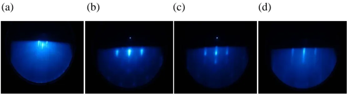
the graded Zn1-xCdxO using different excitation (325 nm and 377 nm). (d) White PL emission can be observed by naked eye………...65
7.4 PL spectra of the graded Zn1-xCdxO film at various temperatures. The inset shows integrated PL intensities as a function of temperature for the graded Zn1-xCdxO film……….66 7.5 (a) PL intensity decay as a function of temperature. (b) PL decay time and
stretching exponent (β) of graded Zn1-xCdxO as a functions of temperature. (c) Temperature dependence of measured PL decay time along with the extracted
radiative and nonradiative lifetime parameters. The transition temperature TTR is
1
Chapter 1
Introduction
Recently, ZnO-based optoelectronic devices have attracted increasing attentions
due to their attractive properties of the wide band gap (3.37 eV) and high exciton
binding energy (60 meV) [1].In addition, ZnO has certain advantages, including the
availability of fairly high quality ZnO bulk single crystals and the amenability to wet
chemical etching [2-4]. For the development of ZnO-based optoelectronic devices,
such as light emitting diodes, solar blind photo detectors, and transparent thin film
transistors [5-9], the growth of high quality ZnO-based ternary compounds and
quantum well structures is crucial. Molecular beam epitaxy (MBE) is one of best
growth techniques to grow such structures. MBE operates in ultra-high vacuum
condition, which allows a slow deposition rate and the observation of in-situ growth
by reflection high energy electron diffraction (RHEED). By this way, films and
quantum structures of high quality could be grown. In addition, many molecular
sources can be installed in a typical MBE system. As a result, novel binary, ternary
and quaternary compound semiconductors with good crystal quality can be prepared.
In this thesis, MBE technique was used to grow the ZnO, Zn1−xMgxO, Zn1−xMnxO and Zn1−xCdxO. The optical properties of these materials were studied.
2
In chapter 2, the MBE growth technique was described. The optical spectroscopy,
which includes the photoluminescence, transmittance, and time-resolved
photoluminescence used to investigate the optical properties were presented. The
growth conditions of all samples in this thesis were also shown.
In chapter 3, ZnO and Zn1−xMgxO epitaxial films were grown on c-plane
sapphire substrates using MgO buffer layers. Presently, sapphire is the most
commonly used substrate for ZnO-based epitaxial growth. Since sapphire has the
advantages of thermal stability at high growth temperature, chemical inertness, strong
bond strength. However, the lattice mismatch between ZnO and sapphire is 18.4 %
[10].For that reason, the ZnO films generally show rough surface morphology and
poor crystal quality when ZnO films are directly grown on c-plane sapphire substrates
without a buffer layer. MgO is the most widely used buffer layer for ZnO grown on
sapphire substrates, because the lattice mismatch between ZnO and MgO reduce to
8.4 % [11].Nowadays, the wavelength for emission or detection can be tuned by
using either ZnO quantum well or by alloying ZnO with a higher band gap material.
MgO has a band gap of about 6.7 eV. Though the equilibrium solid solubility of MgO
in ZnO in the bulk form is limited (less than 4 mol. %), but the ionic radii of Mg2+ (0.057 nm) is similar to that of Zn2+ (0.060 nm) [12]. Since MBE is a non-equilibrium processing technique, solid solubility of MgO in ZnO can be significantly enhanced in
3
the metastable state after thin film deposition. Thus, we report the growth and optical
properties of ZnO and Zn1−xMgxO thin films grown on c-plane sapphire substrates
using MgO buffer layers in this thesis.
In chapter 4, the growth and optical property of Zn1−xMnxO thin film was
described. Diluted magnetic semiconductors (DMS) have been intensely studied in the last few decades. By introducing the magnetic atoms to substitute the cations of
the binary semiconductors, such as II-VI or III-V compound semiconductors, the band
gaps can be varied and the semiconductors also exhibit very interesting magnetic
effects [13]. Among II-VI DMS, Zn1−xMnxO has direct band gap (above 3.37 eV at
300 K) and large exciton binding energy (near 60 meV). Furthermore, Mn2+ ion has half-filled 3d-orbital with five electrons in the same spin direction, therefore it has the
large total spin angular momentum (S = 5/2). These advantages make Zn1−xMnxO a
potential material for applications in spintronics such as spin light-emitting diodes
(spin LEDs) and spin filters. Recently, there are some papers focused on the magnetic
properties of ZnMnO because of the prediction of room temperature ferromagnetism
[14], however optical properties of ZnMnO are still rarely studied. Therefore, in this
thesis, resonant Raman scattering and photoluminescence of ZnMnO with variant Mn
concentration are investigated.
4
were depicted. For visible emission, Zn1−xCdxO is a suitable compound for extending
emission wavelength from ultraviolet to blue and green spectral regions owing to the
smaller band gap of CdO of 2.3 eV [15]. In addition, the fabrication of ZnO/Zn1−xCdxO heterojunctions and multiple quantum wells would provide the key
element in ZnO-based light emitting diodes and laser diodes. However, the rock-salt structure of CdO is dissimilar to the wurtzite structure of ZnO, which induces
problems for ZnCdO alloys, such as poor crystalline quality. Up to date, Zn1−xCdxO
film had been recently prepared by pulse-laser deposition [16], metal organic
chemical vapor deposition (MOCVD) [17-18], and MBE [19]. In comparison, MBE
distinguished by its high versatility and the capability of in situ growth control.
However, the results about the fabrication and optical properties of Zn1−xCdxO films grown by MBE are still rather limited. Sadofev et al. [19] demonstrated single-phase
Zn1−xCdxO layers with Cd composition up to 32 % by MBE. Although, the Cd
composition in Zn1−xCdxO films exceeds x=32 %, which is much less than that was grown by MOCVD (69 %) [18]. Therefore, in chapter 5, 6 and 7, we represent the
growth approaches to fabricate high quality Zn1−xCdxO films with high Cd concentration and visible light emission using MBE. Detailed studies of temperature
dependent PL and TRPL of Zn1−xCdxO films with different concentration of Cd are also reported. Finally, a brief conclusion will be presented in chapter 8.
5
Chapter 2
Experimental details
In this chapter, the experimental techniques used in this thesis were described.
The experimental techniques include plasma-assisted molecular beam epitaxy
(PA-MBE), photoluminescence (PL) spectroscopy, transmittance (T), time-resolved
photoluminescence spectroscopy (TRPL). The growth conditions of all samples will
be listed.
2.1 MBE system
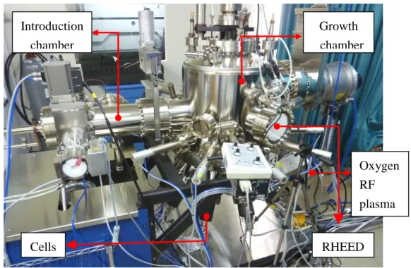
The SVT Associates MBE system is shown in Fig. 2.1. It consists of a vertical
growth chamber with ten cell ports, a load-lock chamber, and analytical equipments.
Currently, six solid sources Zn, Mn, Cd, Mg, Se, Te, and gas source (Oxygen),
are installed in the effusion cells and plasma cell. Each source has its own shutter to
control the supply duration of each source. The samples were grown on the heated
substrate which was set to rotate for uniform growth and there is a main-shutter
between sources and the substrate to avoid the unintentional evaporation before
growth.
6
chamber. Its high vacuum (< 5×10⁻⁸ torr) is achieved by using a diaphragm pump and a turbo pump. The growth chamber was further pumped down to a base pressure of
2×10⁻¹⁰ torr. The reflection high-energy electron diffraction (RHEED) system is also set up in the growth chamber. It is an invaluable tool to determine different aspects of
the deposition layer. Morphological data of the surface may be interpreted from the spot and line pattern, which appear on the phosphor screen display during growth.
2.2 Growth conditions of ZnO
The detailed growth conditions of ZnO thin films are listed in Table 2.1. Fig.
2.2 shows the growth rates of ZnO thin films with various Zn cell temperatures. When
the substrate temperature was fixed at 650 ℃ and the oxygen flow rate was 0.6
SCCM with plasma power 250 W, the growth rate increases linearly with the
increasing Zn cell temperature, which indicates these ZnO thin films were grown
under oxygen-rich conditions.
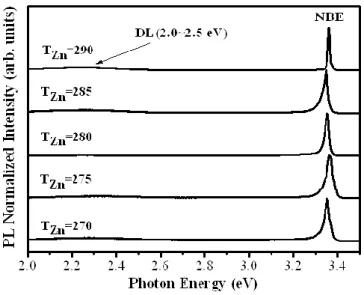
The PL spectra of ZnO thin films with various Zn cell temperatures at 10 K are
shown in Fig. 2.3. For these samples, the dominant peaks around 3.36 eV are
attributed to the near band edge (NBE) emission [20]. The broad and weak emissions
which originate from the deep levels (DLs) near 2.25 eV are also observed. The DLs
are attributed to the zinc interstitial (Zni), oxygen vacancy (Vo) [21], and oxygen
7
emission. The intensity ratio reaches maximum value of 75 at Zn cell temperature of
280 ℃. This growth condition was used for the growth of Zn1-xMgxO, Zn1-xMnxO and
Zn1-xCdxO epilayers.
2.3 Growth condition of Zn1-xMgxO
The structure of the Zn1-xMgxO thin films used in chapter 3 was shown in Fig.
2.5. The detailed growth conditions of Zn1-xMgxO thin films are listed in Table 2.2.
2.4 Growth condition of Zn1-xMnxO
The structure of the Zn1-xMnxO thin films used in chapter 4 was shown in Fig.
2.6. The detailed growth conditions of Zn1-xMgxO thin films are listed in Table 2.3.
2.5 Growth condition of Zn1-xCdxO
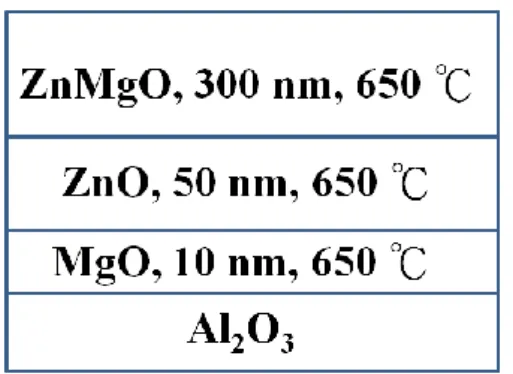
The structure of the Zn1-xCdxO thin films used in chapter 5~7 was shown in Fig. 2.7. The detailed growth conditions of Zn1-xCdxO thin films are listed in Table 2.4. 2.6 Photoluminescence spectroscopy
To study optical properties of semiconductors, laser beams with photon energy
higher than the band gap energy of the semiconductor are usually used to excite
electrons from the valence band to the conduction band and leave holes in the valence
band. The excited electrons/holes relaxed to the bottom of conduction band/top of the
8
exciton by Coulomb interaction. Electrons and holes, Excitons, recombine and emit
photons. The emitted photons can be detected and analyzed by photoluminescence
(PL) spectroscopy.
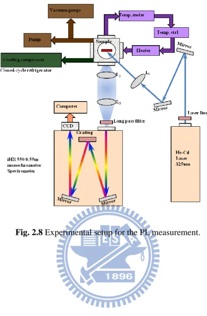
The experimental set-up for the PL measurement is shown in Fig. 2.8. PL
measurements were performed by using the 325 nm line of a He-Cd laser. The
incident beam was focused by a lens (f=10 cm). The PL emission from sample was
collected by second lens (f=10 cm) and focused by the third lens (f=30 cm) to the
spectrometer. The signal was dispersed by an iHR550 spectrometer and detected by
liquid nitrogen cooled charge-coupled device (CCD). The spectrometer was
controlled by a computer, which was used to store and plot the collected data. For
temperature-dependent PL measurements, samples were cooled in a closed-cycle
refrigerator system. The temperature was varied from 10 K to 300 K.
2.7 Transmittance
The experimental set-up for transmittance measurement is shown in Fig. 2.9. A
broadband xenon lamp was used as an excitation source. The incident beam was
focused on the sample by a lens (f=10 cm). The transmittance beam from the sample
was collected to the entrance slit by lens L2 (f=10 cm) and L3 (f=30 cm). The
9 liquid nitrogen cooled charge-coupled device.
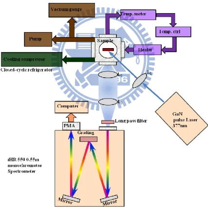
2.8 Time-resolved photoluminescence spectroscopy
TRPL system was used to study the decay dynamics of excitons. The
experimental setup of TRPL system is similar to the PL system and shown in Fig. 2.10.
The GaN diode laser with 50 ps pulses and a repetition rate of 40 MHz at a
wavelength of 377 nm was used as an excitation source. The peak power of the pulse
was estimated to be below 0.1 mW. The laser beam was focused on the sample by a
lens (f=10 cm). The combination lenses guide the signal to the iHR550 spectrometer,
which was equipped with a high-speed photomultiplier tube to detect the signal. The
signal was further analyzed by a computer. The overall temporal resolution of the
10 T (substrate) (℃) T (Zn) (℃) O2 plasma (SCCM/W) Thickness (nm) Sample 1-A 650 270 0.6/250 131 Sample 1-B 650 275 0.6/250 144 Sample 1-C 650 280 0.6/250 159 Sample 1-D 650 285 0.6/250 181 Sample 1-E 650 290 0.6/250 225
Table 2.1 Growth conditions of ZnO thin films.
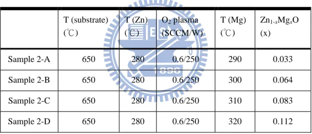
T (substrate) (℃) T (Zn) (℃) O2 plasma (SCCM/W) T (Mg) (℃) Zn1-xMgxO (x) Sample 2-A 650 280 0.6/250 290 0.033 Sample 2-B 650 280 0.6/250 300 0.064 Sample 2-C 650 280 0.6/250 310 0.083 Sample 2-D 650 280 0.6/250 320 0.112
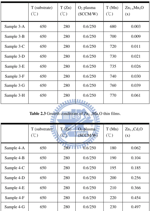
11 T (substrate) (℃) T (Zn) (℃) O2 plasma (SCCM/W) T (Mn) (℃) Zn1-xMnxO (x) Sample 3-A 650 280 0.6/250 680 0.003 Sample 3-B 650 280 0.6/250 700 0.009 Sample 3-C 650 280 0.6/250 720 0.011 Sample 3-D 650 280 0.6/250 730 0.021 Sample 3-E 650 280 0.6/250 735 0.026 Sample 3-F 650 280 0.6/250 740 0.030 Sample 3-G 650 280 0.6/250 760 0.039 Sample 3-H 650 280 0.6/250 770 0.061
Table 2.3 Growth conditions of Zn1-xMnxO thin films.
T (substrate) (℃) T (Zn) (℃) O2 plasma (SCCM/W) T (Mn) (℃) Zn1-xCdxO (x) Sample 4-A 650 280 0.6/250 180 0.062 Sample 4-B 650 280 0.6/250 190 0.104 Sample 4-C 650 280 0.6/250 195 0.185 Sample 4-D 650 280 0.6/250 200 0.256 Sample 4-E 650 280 0.6/250 210 0.366 Sample 4-F 650 280 0.6/250 220 0.454 Sample 4-G 650 280 0.6/250 230 0.497
12
Fig. 2.1 MBE system.
Fig. 2.2 Growth rates of ZnO thin films as a function of Zn cell temperatures. Growth chamber Introduction chamber chamber Cells RHEED Oxygen RF plasma
13
Fig. 2.3 Low temperature (10 K) PL spectra of ZnO thin films with various Zn cell temperatures.
Fig. 2.4 The intensity ratios of the NBE emission to the DL emission for ZnO thin films as a function of Zn cell temperatures.
14
Fig. 2.5 Sample structure of Zn1-xMgxO thin films.
Fig. 2.6 Sample structure of Zn1-xMnxO thin films.
15
16
Fig. 2.9 Experimental setup for the transmittance measurement.
17
Chapter 3
Growth and characterization of Zn
1-xMgxO thin films and
ZnO/ZnMgO multiple quantum wells
In this chapter, growth and characterization of Zn1-xMgxO (x=0~0.112) thin films
grown by molecular beam epitaxy system will be discussed. The MgO buffer is very
useful for the improvement of surface morphology during the initial growth stage,
which eventually leads to an atomically flat surface. Additionally, ZnO/ZnMgO
multiple quantum wells (QWs) were also fabricated successfully and their optical
properties were investigated.
The morphology evolution can be observed by in situ reflection high-energy
electron diffraction (RHEED). At the beginning of MgO deposition, the sharp streaky
pattern of clean Al2O3 substrates, as shown in Fig. 1 (a), becomes diffuse spotty
pattern, as shown in Fig. 1 (b), because of the large (8%) lattice mismatch between
MgO(111) and Al2O3 (0001). Therefore, the growth of MgO is a 3-dimensional
growth mode. Immediately after the growth of MgO buffer layer, the ZnO growth
starts with spotty patterns, as shown in figure 1 (c), superimposing on the MgO
patterns with the spot spacing about 9% smaller. As the growth continues, the
18
procedure can be dramatically accelerated by interrupting the deposition and
annealing the sample at 750 °C. After 5 min annealing, Fig. 1(d) shows sharp streaky
RHEED patterns of ZnO. Thus, a flat surface of buffer layer was accomplished. The
growth of Zn1-xMgxO epilayers then starts at 650 °C, with the same oxygen flow rate
of 0.6 sccm under the plasma power of 250 W as MgO and ZnO buffers. The Zn cell
temperature is 280℃ and the Mg cell temperatures are varied from 290 to 300, 310,
and 320℃ for the growth of Zn1−xMgxO thin films.
In this study, the Mg content in Zn1−xMgxO was determined by energy dispersive
x-ray spectroscopy. Fig. 2 shows the PL spectra of the Zn1−xMgxO layers recorded at a
temperature of 10 K exhibit a sharp band edge luminescence, which originates from
the recombination of bound excitons. The emission spectra of Zn1−xMgxO films is broadened due to alloying and the related potential fluctuations. Additionally, the
emissions which originate from the deep levels near 2.25 eV are not observed. For
increasing Mg content the excitonic luminescence exhibits blue shift. The maximum
emission energy is 3.71 eV for the Zn0.888Mg0.112O sample. he low-temperature
transmittance spectra of Zn1−xMgxO are also shown in the inset of Fig. 2. The energy of strong absorption edge increases with Mg concentration. It implies the growth of
high quality Zn1−xMgxO thin films with MgO/ZnO buffer layers were achieved.
19
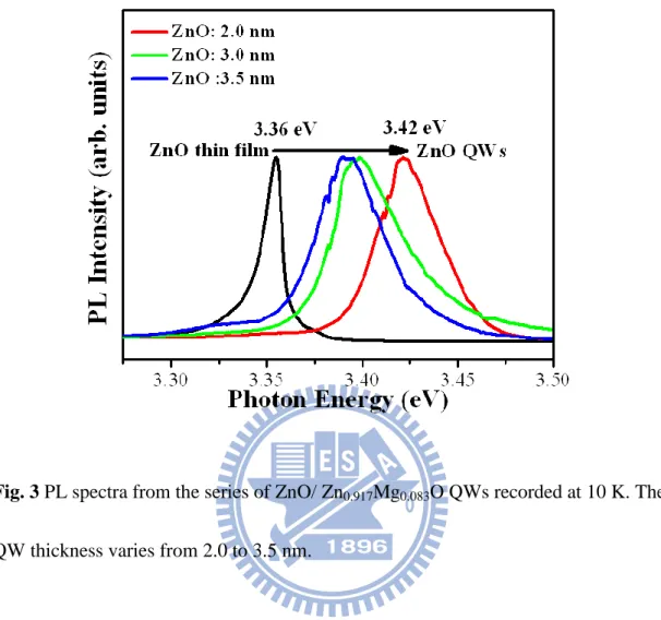
the ZnO/ Zn0.917Mg0.083O multiple QWs. Fig. 3 displays the low-temperature (10K)
PL spectra from the series of QWs with well width from 2.0 to 3.5 nm. The emission
of a donor-bound exciton at 3.36 eV from the ZnO well is clearly identified. The
decrease in emission energy with the increasing well width is owing to the
confinement effect. Additionally, the full width at half maximum of the PL emission
from the ZnO well with 2 nm(~50 meV) is narrower than previous reports(~60 meV)
[23]. Thus the quality of ZnO/ZnMgO multiple QWs is comparable to that was used
to fabricate ZnO/ZnMgO multiple QW based high-efficiency light emitting diodes.
In conclusion, high quality Zn1-xMgxO (x=0~0.112) thin films were grown
by PA-MBE. The MgO buffer is very effective for the improvement of surface
morphology during the initial growth stage, which eventually leads to an atomically
flat surface. The energy of absorption edge increasing with Mg concentration was
20
(a) (b) (c) (d)
Fig. 1 RHEED patterns show the surface morphology evolution during growth. (a)
The Al2O3 (0001) surface after oxygen plasma treatment. (b) Growth of MgO buffer
layer starts. (c) and (d) respectively correspond to ZnO surfaces before and after
21
Fig. 2 PL spectra of the Zn1-xMgxO films (0≦x≦0.112) at 10 K. The inset shows the transmittance spectra of Zn1-xMgxO at 10 K.
22
Fig. 3 PL spectra from the series of ZnO/ Zn0.917Mg0.083O QWs recorded at 10 K. The
23
Chapter 4
Growth and optical Properties of Zn
1-xMnxO thin Films
In this chapter, optical properties of Zn1-xMnxO (x=0~0.061) thin films will be
studied by transmittance, resonance Raman scattering and circular polarization
measurements.
Figure 1(a) shows room temperature transmittance spectra of Zn1-xMnxO thin
films with Mn concentration x=0, 0.009, 0.030 and 0.061. The absorption edge energy
increasing with Mn concentration can be observed. Additionally, the absorption edge
broadening is assumed as E(band-maximum) - E(absorption edge). The broadening is
because of the generation of disorder in the semiconductor, this causes some localized
states [24].Compared with the absorption edge broadening published in some papers
(from 90 to 140 meV) [25-26], the absorption edge broadening of our samples (from
20 to 35 meV) are narrower. It means that there is high quality in our samples. Figure
1(b) shows the absorption edge energy of the Zn1-xMnxO versus Mn concentration. The blue shift of the absorption energy is due to MnO having a larger band gap than
ZnO [27]. The shift of the absorption edge can be expressed by the following equation
x 3.337 3.056x
eVE (1).
24
broadening of the absorption edge increases with the Mn concentration. The
broadening is mainly due to the increasing disorder with increasing Mn concentration
in Zn1-xMnxO. There are also strong mid-gap absorptions around 3 eV for higher Mn
concentration samples. This effect has been ascribed to the transition involves d
orbital of the Mn2+ ion [28].
Figure 2 shows low temperature (10 K) resonant Raman scattering (RRS) spectra
of ZnO and Zn0.97Mn0.03O thin films using the He-Cd laser (λ=325 nm) excitation.
RRS experiment is performed under the excitation laser energy higher than the band
gap, and the incident photon energy will be in resonance with the electronic interband
transition. The peak at 578 cm-1 is the first-order longitudinal optical (LO) phonon mode [29], in which both O and Zn atoms vibrate in the same direction. The weak
peak around 457 cm-1 is ascribed to the E2 (high) mode. Compared with 440 cm-1 in
bulk ZnO single crystal [29], the frequency of the E2 (high) mode in our sample is
slightly larger, it is mainly due to strain effect in the thin film. Under RRS condition,
some intense peaks at frequency positions of approximately integer times 578 cm-1 contribute to the nth-order LO phonon scattering processes. These are intense LO
phonon lines because of the Frohlich interaction, which is the interaction between
electrons and the longitudinal electrical field induced by the LO phonons [30]. In
25
these LO phonon modes. Interestingly, the intervals of these weak peaks are also close
to the frequency of LO phonon mode. Considering the frequency positions of these
peaks, they are probably caused by the combination of E2 (high) mode and multiple
LO phonon scattering.
From the RRS spectra, we find 5 and 11 LO phonon modes for ZnO and
Zn0.97Mn0.03O samples, respectively. In previous studies [31], J. F. Scott et al reported
that the LO phonon numbers (n) in RRS spectra varies proportionally with the
electron-phonon coupling coefficient (α), which is given as the ratio of the Frohlich
interaction energy to the LO phonon energy. They also predicted the number of LO
phonon modes in ZnO is more than n=9 in CdS. However, they only found n=8 in
their ZnO sample. From our results, we could not find LO phonon lines for n>5 in
ZnO due to the strong near band edge PL emission. However, for Zn0.97Mn0.03O, the
near band edge emission is weak and due to the large electron-phonon coupling
coefficient α=0.9 (is assumed to be the same as ZnO), the observation of large
amount of LO phonon lines (n=11) in RRS spectra can be understood.
Figure 3 shows the RRS spectra of Zn1-xMnxO (x=0.003~0.030) thin films. Besides some intense LO phonon lines, there is an extra peak at 3632 cm-1 for Zn0.997Mn0.003O sample. This peak is ascribed to the neutral donor bound exciton
26
frequency position of around 3500 cm-1, which is assigned to the sixth-order LO phonon mode, is always the largest in each of Zn1-xMnxO samples, and the intensity
decreases with increasing Mn concentration. The behavior of intensity variation is
mainly related to the band gap position, and it can be explained by using the Raman
cross section for the nth-order LO phonon mode which is given as [32]
0 B LO 2 0 m LO 4 n T k ω exp Γ ω ω m E g, m e, m e, n g, μ ω σ j j j ex j j (2),where μ is the electronic transition dipole moment, Eex is the electronic transition energy. i and LO are the energies of the incident photon and the LO phonon,
respectively. is the homogeneous line width. g,n j and g, j are the (n+j)
th-order and jth-order LO phonon states in the electronic ground state, respectively.
m
e, is the mth-order LO phonon state in the electronic excited e state. kB is Boltzmann’s constant and T is the temperature. From this equation, the nth-order LO phonon mode intensity will become larger if Eg i nLO. The band gap of
Zn1-xMnxO shifts to higher energy when Mn concentration increases, and it tends to be away from the frequency position of around 3500 cm-1. Therefore, the intensity of sixth-order LO phonon mode decreases.
To investigate the dependence of RRS intensity on the band gap energy,
temperature dependent RRS spectra of Zn0.991Mn0.009O is shown in figure 4(a). At 10
27
However, when the temperature increases to 160 K, the seventh-order LO phonon
mode around 4100 cm-1 becomes the largest in intensity. The behavior can be explained by considering the temperature dependence of the photoluminescence (PL).
Figure 4(b) shows the PL peak position of Zn0.991Mn0.009O as a function of the
temperature, and the curve can be fitted by considering the Bose-Einstein statistical
factor for phonons[33]
1 / exp 2 0 T a E T E B (3),where E
T and E
0 are the energies at T K and 0 K, respectively, a is the Bstrength of the electron-phonon interaction, and is associated with the mean
frequency of the phonons. From figure 4(a) and (b), the shift of PL position results in
the LO phonon line intensity variation. To summarize, multiple LO phonon scattering in RRS spectra can be explained by using the “cascade model” [34-35], the scattered photons will have energy i nLO or i n E n LO
high ) ( 2 .
Moreover, by studying RRS spectra, we find that when the scattered photon energy is
close to the band gap, the LO phonon intensity will be resonantly enhanced.
Figure 5 show the low temperature (10 K) PL spectra of Zn0.997Mn0.003O
analyzed by
and
circular polarization at magnetic field B = 0 and B = 5Tesla. At B = 0, no difference was observed between two circular polarization. The
28
and
components are approximately the same. However, at B = 5 Tesla, a slightdifference is observed between the two circular polarization components of the D0X.
While the intensities of the two circular polarization components of the RRS remain
the same. The degree of circular polarization can be defined as
I I I I P (4),
where Iσ and Iσ are the intensities of the right and left circular polarization,
respectively. For RRS, P = 0 at B = 0 and 5 Tesla. Whereas, for D0X emission, P = 0
at 0 Tesla and P = 9 % at 5 Tesla. The non-zero circular polarization is due to the
energy splitting of the two spin components of the D0X, (electron -1/2 and hole -3/2)
and (electron +1/2 and hole +3/2). Although, the energy separation is too small to be
resolved, due the energy relaxation from the higher energy spin state to the lower
energy spin state, P=9 % is observed. The dependence of circular polarization on the
magnetic field shows Brillouin-type para-magnetism. No hysteresis is observed. It
implies that the Zn0.997Mn0.003O exhibits para-magnetism due sp-d exchange
interaction between conduction band s electrons/valence band p electron and d
electrons of the Mn atoms.
In summary, we have grown Zn1-xMnxO (x=0~0.061) thin films by PA-MBE. Transmittance measurement shows an increase of the band gap with the increasing
29
order for ZnO and ZnMnO samples, respectively. From the temperature dependent
RRS experiment, we find the intensities of these LO phonon lines are sensitive to the
band gap position. Low temperature PL spectra of Zn0.997Mn0.003O at magnetic field
B=0 T and 5 T were investigated to calculate the degrees of circular polarization of
30
Fig.1 (a) Room temperature transmittance spectra of Zn1-xMnxO thin films with Mn
concentration x=0, 0.009, 0.030 and 0.061. (b) The energy of absorption edge for
Zn1-xMnxO thin films as a function of the Mn concentrations(x). The experimental results of ours(□) and reference 24 (■) are plotted.
31
Fig. 2 Resonant Raman scatterings of ZnO and Zn0.97Mn0.03O thin films, using the
32
Fig. 3 Resonant Raman scatterings of Zn1-xMnxO thin films, using the He–Cd laser
33
Fig. 4 (a) Resonant Raman scatterings of Zn0.991Mn0.009O thin films with variable
temperature, using the He-Cd laser (λ = 325 nm). The arrows show the PL positions.
(b) Temperature dependent PL position of Zn0.991Mn0.009O. The solid curve describes
the fit of these data by using the Bose-Einstein statistical factor for phonons. The
dashed lines represents the energy positions of the scattered photons with energy
LO i n
34
Fig. 5 Low temperature (10 K) PL spectra of Zn0.997Mn0.003O for B = 0 and B = 5
35
Chapter 5
Thermal-activated carrier transfer in Zn
0.98Cd
0.02O thin film
In this chapter, the thermal-activated carrier transfer processes in Zn0.98Cd0.02O
thin film grown by plasma-assisted molecular beam epitaxy were investigated by
temperature dependent and time-resolved photoluminescence.
Fig. 1 shows the PL spectra of ZnO and Zn0.98Cd0.02O films at 10 K. The
emission peaks at 3.361 and 3.366 eV were assigned to the excitons bound to neutral
donors (DoX) [36]. The peak at 3.377 eV is attributed to the free A excitons (FXA)
[37]. When Cd atoms were introduced into ZnO, the PL band becomes broad and the
spectral position of the PL peak shifts to 3.185 eV. According to the experimental
results of Gruber et al. [38], the Cd composition herein can be estimated as 2%.
Additionally, the PL emission profile of Zn0.98Cd0.02O is not symmetry due to the
existence of localized states at low energy side. The transmittance spectrum at 10 K
shown in the inset shows a strong absorption near the band edge. It can be seen that
the Cd incorporation reduces the band gap energy and causes a Stokes’ shift of about 100 meV. The Stokes’ shift is attributed to the localization of excitons due to the Cd compositional fluctuation [39]. In order to further investigate and compare the optical
36
ZnO and Zn0.98Cd0.02O were carried out. In Fig. 2 (a), both DoX and FXA of ZnO shift
to lower energies, and the line-width broadens with increasing temperature. The PL
line width broadening is related to the carrier–phonon interaction. Additionally,
because of thermally activated processes of carriers, FX dominates at high
temperature. In Fig. 2 (b), three PL peaks of Zn0.98Cd0.02O labeled as P1, P2, and P3
were observed at different temperatures. The P1 emission was observed at low
temperature. When T>140 K, additional peaks, P2 and P3, become visible. The
intensity of P2 increases and exceeds that of P1 when T>220 K. Similar optical
properties were also observed by Yang et al. [40] in ZnSe1-xTex (x=0.01) epilayers. In
the case of ZnSe1-xTex, at low temperature of 10 K, X/Te is not observed and the PL of the Ten-bound excitons (X/Ten) is very pronounced. The energy states of X/Te and
X/Te clusters become observable as the temperature was increased. Thus, the PL
peaks of P1, P2, and P3 can be attributed to the emissions from X/Cdn, X/Cd, and
X/Cd cluster, respectively. Fig. 2(c) shows the dependence of X/Cdn intensity on
temperature with a double-channels activation energy function: [41]
T k E C T k E C I T I B a B a PL 2 2 1 1 0 exp exp 1 (1).Where IPL(T) is the integrated PL intensity at temperature T, kB is the Boltzmann
constant, Ea1 and Ea2 denote the activation energy, C is a tunneling factor, and I0 is
37
Ea2=19 meV were extracted. The activation energy Ea1 is attributed to the average
localization energy of the X/Cdn. On the other hand, the activation energy Ea2
corresponds to thermal energy of 220 K, which is similar to the quenching
temperature of X/Cdn intensity. Therefore, we consider that the activation energy Ea2
is the energy for carriers transferred from X/Cdn to X/Cd.
In order to confirm the origin of the emissions from X/Cd, X/Cdn, and X/Cd clusters,
the PL peak positions of the free-exciton (FX), X/Cd, X/Cdn, and X/Cd clusters as a
function of temperature were plotted in Fig. 3(a). The FX peak positions obtained
from transmittance are well fitted by the Vashini’s prediction [42] which is written as
T E
T
T
Eg g 0 2 (2).
Where Eg(0) is the band-gap energy at T=0 K, and a and b are the corresponding
thermal coefficients. The fitting is labeled by solid lines in Fig. 3(a). The X/Cd peaks
exhibit a similar trend. The emission energy of X/Cd is 80 meV lower than that of FX.
It implies that there is not enough energy to offer the carriers transferred from X/Cd
states to FX states. Therefore, X/Cd dominates the carrier recombination at 300 K.
However, the X/Cdn peak demonstrates a fast red shift at temperatures above 50 K.
This phenomenon could be attributed to continuous localized states formed with the
X/Cdn states. We proposed that excitons assisted by the scattering of LO phonons
38
process is promoted as the temperature increases because the spreading of exciton
wave-function enhances the interaction with LO phonon fields. In this condition, the
increased temperature only causes small parts of the carriers to delocalize from the
deep localized states to the shallow ones. The X/Cdn peak redshifts dramatically until
the carriers were relocalized at the X/Cd cluster states (the deepest localized states).
On the contrary, as the temperature exceeds 220 K, the thermal energy overthrows the
activation barrier of 19 meV, which pro- motes large amount of the carriers to escape
from the deep localization and the X/Cd emission dominates. Fig. 3(b) shows the
power dependent PL spectra at 220 K for Zn0.98Cd0.02O. The intensity of PL emission
is enhanced with increasing excitation power. Under an excitation power of 65 W/cm2, the emission energies of X/Cd cluster and X/Cd are at 2.782 and 3.160 eV,
respectively. As the excitation power is increased, the X/Cd cluster exhibits energy
blueshift and the X/Cdn state dominates the spectrum. This result implies that the
density of state for the X/Cdn is much higher than that for the X/Cd cluster. The
increasing excitation density saturates the lower energy states. As a result, the X/Cdn
state dominates the emission.
In order to provide further evidence to support the existence of localized states
and to demonstrate the origin of the radiative recombination, we performed TRPL
39
recombination time decreases with increasing temperature. It implies that the
thermalized carriers could relax easily over along distance and find a lower
local-energy minimum. Besides, the main PL peak positions undergoes no obvious
energy shift over time at 10 K, reflecting the main recombination of the localized state
with the same concentration of Cd. However, the main peak shifts 39 meV toward the
low energy side with time at 100 K. It reveals that the thermal- activated carriers
transfer to the deeper localized states via the phonon scattering. As the temperature
increases to 150 K, a larger redshift of 100 meV with the delay time was found,
indicating more carriers can transfer to the deeper localized states. In combination
with temperature-dependent PL and TRPL, we demonstrate the carrier transfer
dynamics in Zn0.98Cd0.02O. The strong redshift of the X/Cdn peak energy is caused by the carrier transfers to the deep localized states as T<220 K. Moreover, a
delocalization process occurs as the temperature exceeds 220K.
In summary, emissions of X/Cd, X/Cdn, and X/Cd cluster from Zn0.98Cd0.02O thin
film were investigated by PL and TRPL spectroscopy. Two emission peaks, which are
attributed to the carrier recombinations of X/Cd states and X/Cd cluster states, were
observed at elevated temperatures. From 50 to 220 K, the carriers transfer from
shallow X/Cdn states to deep localized X/Cdn states. Above 220 K, the carriers escape
40
Fig. 1 PL spectra of ZnO and Zn0.98Cd0.02O films at10 K. The inset shows the PL and
41
Fig. 2 PL spectra of (a) ZnO and (b) Zn0.98Cd0.02O thin films at various temperatures.
(c) Integrated PL intensity of X/Cdn as a function of temperature for Zn0.98Cd0.02O.
42
Fig. 3 (a) PL peak energy trace of X/Cd, X/Cdn, X/Cd cluster and FX at various temperatures. The solid lines are Varshni’s fits. (b) Power dependent spectra of Zn0.98Cd0.02O at 220 K.
43
44
Chapter 6
Growth and carrier dynamics of Zn
1-xCdxO thin films with
visible light emission
In previous chapter, the recombination dynamics of Zn1-xCdxO thin films with
low Cd concentration (x=0.02) sample has been studied. For high efficient light
emitting device application or solar cell application, the growth and optical studies of
high quality Zn1-xCdxO with high Cd concentration are demanded.
In this chapter, high Cd concentration of Zn1-xCdxO was controlled by
adjusting the Cd/Zn beam pressure ratio. The Cd content in Zn1−xCdxO was determined by energy dispersive x-ray spectroscopy and showed concentrations
ranged from 0.062 to 0.497 in Fig. 1. The Cd content, x, increases linearly with
increasing beam equivalent pressure, which was measured by a nude ionization gauge
placed in front of the substrate. It is the first time that Zn1−xCdxO thin film grown at 350°C with Cd composition up to 49.7 % by PA-MBE. During the growth of
Zn0.503Cd0.497O thin film, a streaky RHEED pattern was observed along the (11-2)
azimuth, as shown in the inset of Fig. 1. It implies that Zn0.503Cd0.497O thin film has
smooth surface.
45
increasing x, the luminescence peak shifted to a lower energy from 3.36 eV of ZnO to
1.91 eV of Zn0.503Cd0.497O. It is difficult to grow Zn1−xCdxO with high Cd content.
Because, ZnO and CdO have different crystal structure and the growth temperatures
are very different [43]. Furthermore, there is a large lattice mismatch between ZnO
and CdO. It is the first time that high quality Zn1−xCdxO thin film can be grown at
350°C with red PL peak emission by PA-MBE. Figure 2(b) shows the measured and
referred values of PL peak position versus Cd content x. The solid line,
35 . 3 05 . 1 x EPL (eV) (1),
connects the band gaps of the two binary compounds, ZnO (3.35 eV) and CdO (2.20
eV) [43].
The red dashed line,
2 43 . 6 12 . 6 36 . 3 x x EPL (eV) (2),
describes our experimental data for the PL emission peaks. For comparison, the PL
results summarized from previous reports [38,44-45], can be illustrated by the dotted
line of the following equation,
2 14 . 8 19 . 9 35 . 3 x x EPL (eV) (3).
The deviation from the solid line, band bowing, is due the composition fluctuation
(chemical disorder), which creates local potential well to lower the emission energy.
46
samples have better crystal quality with less chemical disorder.
In order to further investigate the optical properties of Zn1−xCdxO to study the
band bowing effect, temperature-dependent PL measurements of Zn1−xCdxO with x=
0.062, 0.185, 0.366 and 0.454 were carried out. In Fig. 3, the near band edge emission
of Zn0.938Cd0.062O simply shifts to lower energy and the line-width broadens with
increasing temperature. However, the PL peak position of Zn0.815Cd0.185O shows
abnormal red-blue-red shift with increasing temperature. A red shift is observed at
temperature below 90 K. As the temperature is increased above 90K, the PL peak
position shifts to higher energy first, then moves towards lower energy as the
temperature is increased above 120K. In the case of Zn0.634Cd0.366O and
Zn0.546Cd0.454O, the dependence of peak position on temperature shows initial
red-shift and then blue-shift as large as several tenth meV. These novel temperature
behaviors of PL emission peak are attributed to the existence of complex localized
states, X/Cdn and X/Cd clusters, as described in previous chapter. For Zn0.815Cd0.185O ,
due to insufficient thermal energy for localized carriers to overcome the localization
potential at low temperature, they relax to the lower-lying localized states prior to
recombination. As the temperature increases localized carriers are thermalized,
occupy higher energy states and leads to blue shift in emission peak. At temperature
47
over the blue shift. The PL peak position of Zn0.634Cd0.366O and Zn0.546Cd0.454O
demonstrates red-blue (V-shaped) shift with increasing temperature. The red shift
observed at temperature below 100 K and 120 K respectively, and then the blue shift
behavior is observed. Similar optical trends were also observed by Lin et al. in
ZnSe1-xTex (x=0.05) epilayers [46]. In the case of ZnSe0.095Te0.05,the V-shaped energy
shift over the same range of temperatures (10–300 K) are ascribed a rather deep
localization. Additionally, the Stokes’ shift of Zn0.634Cd0.366O and Zn0.546Cd0.454O
shown in Fig. 2(b) is as large as 1 eV. Thus, V-shaped energy shift of Zn0.634Cd0.366O
and Zn0.546Cd0.454O indicates that the carriers are still localized in localized states at
room temperature.
The PL peak positions of Zn0.938Cd0.062O, Zn0.815Cd0.185O, and Zn0.634Cd0.366O, as
a function of temperature were plotted in figure 4(a). The PL peak positions of
Zn0.938Cd0.062O are well fitted by the Vashini’s prediction which is written as
T E
T
T
Eg g 0 2 [42], where Eg(0) is the band-gap energy at T=0 K, and
α and β are the corresponding thermal coefficients. The fitting is labeled by dashed lines in Fig. 4(a). However, the Vashini’s trends don’t completely agree the trends of the PL peak positions in Zn0.815Cd0.185O and Zn0.634Cd0.366O as a function of
temperature. It implies the existence of carrier transfer between localized states. In
48
in Zn1−xCdxO crystal with high Cd concentration [47]. Similar localized states were
also observed by Yang et al.in ZnSe1-xTex epilayers., the localized states of ZnSe1-xTex
include the Ten bound exciton and the Ten clusters bound exciton [40]. Therefore, the
PL emission of Zn0.815Cd0.185O and Zn0.634Cd0.366O can be attributed to the emissions
from the Cdn bound exciton and the Cdn clusters bound exciton, respectively. The Cdn
bound exciton has been identified here as the exciton bound to two or more isolated
Cd. Thus, the localized states with different localized energy were caused the Cdn
bound exciton. On the other hand, the Cdn clusters bound exciton has been identified
here as the exciton bound to the deepest localized states. Fig. 4(b) shows the
temperature dependence of the integrated PL intensity for Zn0.938Cd0.062O,
Zn0.815Cd0.185O, and Zn0.634Cd0.366O. The integrated PL intensity shows a typical
behavior for thermally activated nonradiative recombinations of Zn0.938Cd0.062O. The
integrated PL intensity of the Zn0.815Cd0.185O with increasing temperature first
decreases fast below 40 K, then slows down between 40 and 60 K, and finally
decreases quickly again for T higher than 60 K. On the contrary, the integrated PL
intensity of the Zn0.634Cd0.366O with increasing temperature first decreases below 150
K, then increases above 150 K. Similar optical properties were also observed in
quantum dots system [48]. As a result, thermally activated transfer of carriers was in
49
integrated PL intensity in Zn0.634Cd0.366O can be attributed to the carrier transition
from Cdn clusters to Cdn bound exciton. Fig. 4(c) shows the dependence of the
integrated PL intensity in Zn0.634Cd0.366O on temperature with an activation energy
function:[41]
T k E C I T I B a PL exp 1 0 (4),where IPL(T) is the integrated PL intensity at temperature T, kB is the Boltzmann
constant, Ea denotes the activation energy, C is a tunneling factor, and I0 is the
integrated intensity at the low temperature limit. In this study, Ea=15 meV was
extracted. The activation energy Ea corresponds to thermal energy around 150 K,
which is similar to the temperature that PL peak positions start to blue shift and
integrated PL intensity increases. When the temperature exceeds 150 K, the PL
quenching of Cdn clusters bound exciton and the PL increasing of Cdn bound exciton
becomes dominant.
In summary, this study investigated the growth and carrier dynamics of
Zn1-xCdxO. High quality Zn1-xCdxO thin films with visible light emission were grown on sapphire substrates by PA-MBE. The maximum concentration of Cd is 49.7 %
which can be systematically adjusted via the Cd/Zn beam pressure ratio. The
S-shaped dependence of the PL peak positions indicates that Cdn bound exciton lead
50
energy in high Cd concentration Zn1-xCdxO indicates that Cdn clusters bound exciton,
in which the carriers are deeply trapped below 150 K. Above 150 K, the carriers can
escape from the deepest localized Cdn clusters states to shallow localized Cdn states.
An activation energy Ea=15 meV was observed for Zn0.634Cd0.366O, and the
corresponding thermal energy around 150 K, coincides the temperature where the
51
Fig. 1 Cd content increases linearly with the increasing Cd/Zn beam pressure ratio.
The inset shows the RHEED pattern of Zn0.503Cd0.497O taken along the (11-2)
52
Fig. 2 (a) PL spectra of the Zn1-xCdxO films (0≦x≦0.497) at 10 K. (b) PL peak energy of Zn1-xCdxO as a function of Cd content x.
53
Fig. 3 PL spectra of Zn1-xCdxO with x= 0.062, 0.185, 0.366 and 0.454 at various temperatures.
55
Fig. 4 (a) PL peak energy of Zn0.938Cd0.062O, Zn0.815Cd0.185O, and Zn0.634Cd0.366O at
various temperatures. The dotted line is the Varshni’s fit. (b)Integrated PL intensity as
a function of temperature for Zn0.938Cd0.062O, Zn0.815Cd0.185O, and Zn0.634Cd0.366O. (c)
Integrated PL intensity as a function of temperature for the Zn0.634Cd0.366O. The dotted
56
Chapter 7
Optical properties of the graded Zn
1-xCdxO film
In previous chapters, growth and optical properties of Zn1−xCdxO thin films with
x=0~0.497 were discussed. In this chapter, PL, transmittance, and TRPL spectroscopy
techniques will be employed to study the recombination processes in graded band-gap
Zn1−xCdxO (x=0~25.9%) multilayers for possible applications in photonic devices.
The sample comprising 4-layers with variable Cd-content was grown on
c-sapphire by PA-MBE. The energy band diagram and the arrangement of the graded
layers are presented in Fig. 1(a). Fig. 1(b) shows the PL spectrum of the graded
Zn1−xCdxO film at 10 K. The emission peak at 3.36 eV is assigned to the excitons bound to neutral donors (DoX) from ZnO. The region of the broad band emission is
from 1.40 eV to 3.2 eV. We propose that the broad band emission exhibit the
near-band edge (NBE) emission and localized states emission of Zn1-xCdxO.
Fig. 2(a) presents the broad band emission from 1.40 eV to 3.2 eV. The
dotted-lines in Fig. 2(a) are the curve fitting of the peak. One dotted line with peak
energy at 2.96eV is due to the NBE emission, and the others are associated with the
emissions of the localized states for the graded Zn1-xCdxO. The peak energies of the localized-state-emissions are 2.61 eV (x=14.7%), 2.43 eV (x =19.2%), and 2.22 eV (x

![HPSH [ 氧化數平衡反應式係數 ]](data:image/gif;base64,R0lGODlhAQABAIAAAP///wAAACH5BAEAAAAALAAAAAABAAEAAAICRAEAOw==)