運用基因演算法於微帶線演進最佳化搜尋以完成微波被動電路與主動電路設計
64
0
0
全文
(2) 運用基因演算法於微帶線演進最佳化搜尋 以完成微波被動電路與主動電路設計 Microwave Passive and Active Circuit Design Using Evolutionary Optimization of Microstrip-Line Elements by Genetic Algorithms. Student:Wei-Chun Lee. 研究生:李維鈞 指導教授:周復芳. 博士. Advisor:Dr. Christina F. Jou. 國 立 交 通 大 學 電機資訊學院 電信學程 碩 士 論 文 A Thesis Submitted to Degree Program of Electrical Engineering and Computer Science College of Electrical Engineering and Computer Science National Chiao Tung University in Partial Fulfillment of the Requirements for the Degree of Master of Science in Communication Engineering June 2005 Hsinchu, Taiwan, Republic of China. 中華民國九十四年六月.
(3) 運用基因演算法於微帶線演進最佳化搜尋 以完成微波被動電路與主動電路設計. 學生:李維鈞. 指導教授:周復芳 博士. 國立交通大學電機資訊學院 電信學程﹙研究所﹚碩士班. 中文摘要. 在這篇論文研究中,以基因演算法微帶線演進最佳化搜尋方式設計微波電 路。電路元件排列型式及微帶線結構尺寸等…皆表示成為一序列的參數型態。接 著再以基因演算法針對這一序列的參數作最佳化搜尋、演進,使其滿足我們預先 制定的電路特性及功能。透過 S 參數的轉換顯現並證實電路的頻域響應特性。文 章內容包含了兩個部分的應用。第一個主題是:以基因演算法於微波被動電路的 設計,包括了雙頻帶通濾波器(Dual-Band Band-Pass Filter)以及極寬頻帶通濾波器 (Ultra Wide -Band Band-Pass Filter)的設計及實作量測。第二個主題是:運用基因 演算法於微波主動電路設計,我們以低雜訊放大器(LNA)作為設計範例,將設計 結果以微波模擬軟體作驗證。經由詳細的基因演算法實行準則及概念分析,再以 實際的設計實作範例,得到符合目標的結果,並且有效地引導、介紹這種設計方 式。電路形式上的限制及多目標搜尋結果都會在最佳化搜尋的過程中詳盡討論 之。這些範例結果證實了本篇文章所提出之方法能夠廣泛地運用在微波電路型式 及結構最佳化設計。 i.
(4) Microwave Passive and Active Circuit Design Using Evolutionary Optimization of Microstrip-Line Elements by Genetic Algorithms. Student:Wei-chun Lee. Advisor:Dr. Christina F. Jou. Degree Program of Electrical Engineering Computer Science National Chiao Tung University. Abstract. Evolutionary optimization of microstrip-line element in microwave circuit design is presented in this paper. Topology and dimensions of microstrip elements are expressed by sets of parameters. The sets of parameters are then optimized by genetic algorithms (GA) to satisfy our circuit performance or specifications. The S-parameters are synthesized to obtain and verify the response of the circuit. The applications discussed include two topics. In the first part, we investigate the microwave passive circuit design using GA: dual-band band-pass filter and ultra wideband band-pass filter synthesis and implement. In the second part, we utilize genetic algorithms in microwave active circuit design: low noise amplifier (LNA) design and simulation. Step-by-step implementation aspects of the GA are detailed, through an example with the object of providing useful guidelines for the synthesis method. Circuit pattern constraints and multi-objective design goals are also implemented and discussed in the optimization process. These results have validated our proposing procedure. ii.
(5) Acknowledgement I would like to express my deepest gratitude to my advisor, Dr. Christina F. Jou for her patient instruction, constructive guidance and invaluable suggestions. I am also grateful to the members of my Master’s degree committee, Professor Chi-Yang Chang and Dr. Cheng-Chi Hu for their generous assistance and valuable comments. Over these years, I have also received support and advice from my friends, Ming-Iu Lai, Wan-Chi Liao and my classmate Jian-Zhi Lee. They always provide me instance support to deal with the problems that I meet. For their help, I must thank them in sincerity. Finally, I would like to give my deepest appreciation to my family and colleagues for their encouragement and patience in my life.. Jeff Lee Hsinchu, Taiwan June, 2005. iii.
(6) Contents Chinese Abstract ........................................................................................................ i English Abstract ........................................................................................................ii Acknowledgement ....................................................................................................iii Contents ................................................................................................................... iv Tables Captions ........................................................................................................ vi Figures Captions ..................................................................................................... vii. Chapter 1. Introduction ............................................................................................ 1. 1.1 Review......................................................................................................... 1 1.2 Motivation ................................................................................................... 2 1.3 Organization ................................................................................................ 5 Chapter 2. GA theories and implement method ........................................................ 6. 2.1 Passive circuit:Filter design method .......................................................... 6 2.1.1 Microstrip elements ........................................................................... 6 2.1.2 Element encoding methods ................................................................ 6 2.1.3 Random initial circuit ........................................................................ 7 2.1.4 Chromosome (circuit pattern) transfer to S-parameter........................ 9 2.1.5 Tournament selection among population .......................................... 10 2.1.6 Reproductive cycle of GA ............................................................... 11 2.1.7 GA operators ................................................................................... 12 2.1.8 General structure of GA................................................................... 16 2.1.9 Termination criteria is met ............................................................... 17 2.2 Other investigation into microwave filter design using GA ........................ 18 iv.
(7) 2.3 Active Circuit:LNA design method .......................................................... 21 2.3.1 Element encode and initial circuit pattern ........................................ 21 2.3.2 Multiple object-functions ................................................................ 22 2.3.3 GA evolutionary process.................................................................. 23 2.3.4 Fabrication constraint of LNA ......................................................... 23 Chapter 3. Passive Circuit Design .......................................................................... 25. 3.1 Dual-band band-pass filter (Dual-BPF) for WLAN..................................... 25 3.1.1 WLAN Dual-BPF’s GA parameter setting in advance ...................... 25 3.1.2 GA for WLAN Dual-BPF optimum solutions ................................... 26 3.1.3 Implementation and measurement of WLAN Dual-BPF ................... 27 3.2 Dual-band band-pass filter (3.4-4.2 GHz, 5.6-6.4 GHz).............................. 30 3.2.1 GA parameter setting and optimum solutions for Dual-BPF (3.4-4.2 GHz, 5.6-6.4 GHz) .......................................................................... 30 3.2.2 Circuit implementation and measurement of Dual-BPF (3.4-4.2 GHz, 5.6-6.4 GHz) ................................................................................... 31 3.3 Ultra wideband band-pass filter (UWB BPF).............................................. 34 3.3.1 UWB BPF’s GA parameter setting in advance ................................. 34 3.3.2 GA for optimum solutions of UWB BPF .......................................... 35 3.3.3 Implementation and measurement of UWB BPF .............................. 36 Chapter 4. Active Circuit Design ........................................................................... 39. 4.1 Low Noise Amplifier (LNA) design ........................................................... 39 4.1.1 LNA’s GA parameter setting ............................................................ 41 4.1.2 GA for optimum solutions of LNA................................................... 42 4.1.3 Circuit implementation and simulation results of 4-6 GHz LNA ...... 43 Chapter 5. Conclusion ........................................................................................... 47. Reference ................................................................................................................ 50 v.
(8) Tables Captions Table.1. Distinction between our proposed method and other EM software methods ………………………………………………………………………………....4. Table.2. Microwave filter design using GA………………………………………….18. Table.3. GA parameter setting of WLAN Dual-BPF…………………………...……25. Table.4. Optimum elements of WLAN Dual-BPF……..…………………………….26. Table.5. GA parameter setting of Dual-BPF (3.4-4.2GHz, 5.6-6.4GHz) .….……...30. Table.6. Optimum elements of Dual-BPF (3.4-4.2GHz, 5.6-6.4GHz)………..…….31. Table.7. GA parameter setting of UWB BPF. Table.8. Optimum elements of UWB BPF .....……………………………………….35. Table.9. GA parameter setting of 4-6GHz LNA ..………...…………………………41. Table.10. Optimum elements of 4-6GHz LNA .……………………………………..42. vi. …………………………..………....34.
(9) Figures Captions Figure.1. GA terminology……………………………………………………………...3. Figure.2. Microstrip elements configuration………………………………………….6. Figure.3. Element encoding method in GA……………………………………………7. Figure.4. The concept of random initial circuits…………….………………………..8. Figure.5. Circuit pattern of random initial circuits………..………………………….8. Figure.6. S-parameter and Object-function……………………………………………9. Figure.7. The fitness-function of population…………………………………………10. Figure.8. The concept of tournament selection………………………………………11. Figure.9. Evolutionary reproduction cycle of GA……………………………………11. Figure.10. The concept of crossover………………………………………………….13. Figure.11. The circuit pattern of crossover…….…………………………………….13. Figure.12. The concept of mutation…………………………………………………..14. Figure.13. The circuit pattern of mutation…….……………………………………..15. Figure.14. General structure of GA in this thesis ……………..…………………….16. Figure.15. The best design of band-pass filter in frequency-response……………...17. Figure.16. Circuit patterns in ref [3]………………………………………………….19. Figure.17. Component shapes in ref [37][48]………………………………………..19. Figure.18. Circuit patterns optimum process in ref [7]………………………………20. Figure.19. Scheme of LNA……………………………………………………………21. Figure.20. LNA element encoding method…………………………………………...22. Figure.21. LNA element encoding and initial circuit parameter…………………….22. Figure.22. LNA frequency-response of S-parameter and object-function………….23. Figure.23. Fabrication constraint of LNA circuit pattern..…………………………..24 vii.
(10) Figure.24. Convergent situation of the GA fitness-function in WLAN Dual-BPF....27. Figure.25. Frequency-response by GA of WLAN Dual-BPF...……………………..28. Figure.26. S 21 measured response of WLAN Dual-BPF... ………………………….28. Figure.27. S 11 measured response of WLAN Dual-BPF…………………………….29. Figure.28. Actual circuit pattern of WLAN Dual-BPF (εr=3.38)…...…………….29. Figure.29. Frequency-response by GA of Dual-BPF (3.4-4.2GHz, 5.6-6.4GHz) …32. Figure.30. Measured frequency-response of Dual-BPF (3.4-4.2GHz, 5.6-6.4GHz).32. Figure.31. Actual circuit pattern of Dual-BPF (3.4-4.2GHz, 5.6-6.4GHz) (εr=3.38)………………………………………………………………..…33. Figure.32. Convergent situation of GA fitness-function in UWB BPF…...………..36. Figure.33. Frequency-response by GA of UWB BPF………………………………..37. Figure.34. Measured frequency-response of UWB BPF….………………………….37. Figure.35. Actual circuit pattern of UWB BPF………………………………………38. Figure.36. Group delay characteristics of UWB BPF………………………………..38. Figure.37. NE334S01 super low noise amplifier (a) package outline. (b) noise parameter. (c) S-parameter……………40. Figure.38. Convergent situation of GA fitness-function in 4-6GHz LNA….………43. Figure.39. 4-6 GHz LNA specification by GA (a) frequency-response. Figure.40. (b) noise figure………………………………...44. 4-6 GHz LNA specification by Microwave-Office (a) frequency-response. (b) noise figure………………………………...45. Figure.41. 4-6GHz LNA circuit pattern………………………………………………46. Figure.42. Circuit pattern constraint in crossover process…………………………..48. viii.
(11) Chapter 1 Introduction This article recommends designing the microwave circuit using Genetic Algorithm (GA), which includes two major parts:passive circuits and active circuits. In the part of passive circuits, we will use GA to design and implement Dual-band band-pass filter and Ultra wideband band-pass filter. In the part of active circuit, we will design the Low noise amplifier with GA and prove it with the microwave simulation software and circuit measurement.. 1.1 Review First of all, designing by microwave circuit theory method in passive and active synthesized process review piece by piece instead of the one that designed by ways of performing algorithms.. (1) Microwave passive circuits (i) Dual-band band-pass filter The most common application in WLAN is Dual-band band-pass filter which includes 2.4GHz and 5.2GHz ISM band. In ref [5], the complex variable s in the frequency domain is replaced by a function of the complex variable z by using Z-transform technique. An analog filter prototype will become discrete-time prototype and a dual -band filter consists of a band-stop filter and a wideband filter in a cascade connection. In ref [29], the dual behavior resonator (DBR) allows the direct design of dual-band resonator, but no circuit models are available for the five-branch. 1.
(12) discontinuities.. (ii)Ultra wideband (UWB) band-pass filter The indoor environment frequency range in 3.1GHz to 10.6GHz, which is a norm made by FCC, has made the engineers pay attention to both the performance and size while designing UWB circuits. In ref [41], UWB band-pass filter consists of microstrip ring filter, which is a kind of dual-mode resonator so it can make the compact configuration. However, this kind of microstrip structure including a lot of T-junctions and curve-lines may cause more errors between circuit design and implementation result, if we lack the accurate models.. (2) Microwave active circuits (i)Low Noise Amplifier (LNA) The traditional design method consults the procedure introduced in ref [18], having included drawing stability circles、constant gain circles and noise figure circles…. They are complex designing ways.. 1.2 Motivation Because introduce and design the circuit structure with higher complexity in the front, we have proposed GA to design the microwave circuit, have simplified the design procedure entirely. GA was proposed by John Holland [1] in 1975 and the algorithm came according the concepts of the nature selection. The next page will introduce some terminologies of GA in Fig.1. Here we present the synthesis of planar passive and active circuit design using the GA in connection with a full-wave analysis. The method is illustrated by the. 2.
(13) design of a Dual-band band-pass filter and an Ultra wideband band-pass filter and LNA applications as well as a microstrip topology and optimization problems. In the examples given, the performance of the GA is compared with the circuit implement、 measurement or simulation.. Gene:Circuit element Chromosome:Circuit pattern. Population:Lots of circuit patterns Parents:Selection from population Children:Reproduction from parents Generation:Iterative process of the above-mentioned Fitness:In terms of fitness-function to pick up the best chromosome Fig.1 GA terminology. We recommend using several kinds of microstrip elements to form the component library of GA procedure. There are four kinds of microstrip elements: transmission-lines、open-stubs、stepped-impedance stubs and short-stubs. Then encode the microstrip to binary-code or real-code parameter modeling, which is so-called gene and then formed chromosome by genes. GA simulated biological evolution when searching the parameter space. The design parameters change according to the same rules as the chromosome set of individuals in an evolutional process. These are reproduction、crossover and mutation. We apply these rules to microwave circuit topology searching and optimizations. Certain circuit elements and properties such as widths and electrical lengths are defined by a set of chromosomes. In doing so the 3.
(14) microwave circuit evolves towards an optimal goal designed by the natural law of the “survival of the fittest”. The goal was defined in advance as S 21、S 11 in passive circuit (Filter) design or others performance specifications. We also make a verification by software, the Microwave-Office and actual circuit implement. Distinction between our research and other EM software simulated methods are listed in Table.1:. Circuit Pattern. Our research GA method. EM software method. Evolutionary optimization. Fixed. Table.1 Distinction between our proposed method and other EM software methods. Compare to the other microwave simulation softwares. In GA method, we put forward circuit patterns variably. Select elements at random in the component library and get the best circuit to solve by ways of evolutionary optimization. The general simulation software is regular circuit pattern and optimize only to characteristic impedance and electrical length. The advantage of GA method that we proposed is the wide range of application. So long as we establish the performance specifications and component library in advance, GA can be arranged and formed the circuit pattern and structure parameters which accord with the performance specifications of design. In microwave active circuit design, there are actually few relevant documents but there are more documents of filter and array antenna using GA methods. Therefore, this research especially proposes with GA and uses evolutionary microstrip element to design LNA. Because the goal factors needed to consider will come than S 21、 S 11 of filter while designing LNA:including gain、stability、noise figure、input matching and output matching…,. we use GA strong capability, multi-object functions of 4.
(15) carrying on every above-mentioned project and the factors are searched. Through the GA design result of LNA, it verifies the function of multi-objects searching, which can extensively apply to other microwave component and circuit design.. 1.3 Organization This thesis is organized as follows : Chapter 2 introduces GA theory and implement method in passive circuit (Filter) design and active circuit (LNA) design. Chapter 3 describes passive circuit design:Dual-band band-pass filter and Ultra wideband band-pass filter design and measurement. In chapter 4, we will present active circuit design (LNA) that is similar to the methods in chapter 3. In chapter 5, we will make conclusions and bring out the fabrication constraint and other novel ideas that can be investigated in the future.. 5.
(16) Chapter 2 GA theories and implement methods 2.1 Passive circuit:Filter design method 2.1.1 Microstrip elements This method consists of 4 microstrip elements in library. They are Transmission -Line (type-1)、 Parallel Open-Stub (type-2)、Parallel Open Stepped-Impedance Stub (type-3) and Parallel Short-Stub. See configuration in Fig.2.. Z0. Z02. l2. Z01. l1. l (Transmission-Line) (Stepped-Impedance Stubs). Z0. l. Z0. (Open Stub). l. (Short Stub) Fig.2 Microstrip element configuration. 2.1.2 Element encoding methods The way to encode these microstrip elements are according to ref [2], it belongs. 6.
(17) to real-coded methods. Real-coded GA will be more efficient than Binary-coded GA, further discussion in ref [16]. Each one includes within gene:Type (modeling of the circuit)、Zo (characteristic impedance) and Theta (electrical length). They form a group of chromosome by n genes and form a group of population by m chromosomes. Fig.3 illustrates the element encoding method. gene-1 (element-1). p o p u l a t i o n | m. gene-2 (element-2). gene-n (element-n). chromosome-1 (circuit pattern-1). Type. Zo. Theta. Type. Zo. Theta. Type. Zo. Theta. chromosome-2 (circuit pattern-2). Type. Zo. Theta. Type. Zo. Theta. Type. Zo. Theta. gene-1 chromosome-m (circuit pattern-m). Type. Zo. gene-2 Theta. Type. Zo. gene-n Theta. Type. Zo. Theta. Fig.3 Element encoding method in GA. 2.1.3 Random initial circuit After establishing performance goal and some parameters in advance, the GA program produces the initial circuit at random between the upper and lower limits of the component structure size and produces the initial circuit in genotype real-coded form at random. Fig.4 shows the genotype parameters of random initial circuit. Fig.5 shows the phenotype (circuit pattern) of random initial circuit.. 7.
(18) p o p u l a t i o n | m. chromosome-1. gene-1. gene-2. gene-n. 2,31.75,135.3. 1,47.34,85.11. 4,78.92,108.8. type=2 type=1 zo=31.75(ohms) zo=47.34(ohms) theta=135.3(deg) theta=85.11(deg). chromosome-m. type1=Transmission-Line zo=[zo-min zo-max] theta=[th-min th-max]. type=4 zo=78.92(ohms) theta=108.8(deg). gene-1. gene-2. gene-n. 1,62.10,90.5. 3,85.1,37.9,47.5,61.8. 2,45.76,160.40. type2=open-stub zo=[zo-min zo-max] theta=[th-min th-max]. type3=stepped-impedance zo1=[zo1-min zo1-max] zo2=[zo2-min zo2-max] theta1=[th1-min th1-max] theta2=[th2-min th2-max]. type4=short-stub zo=[zo-min zo-max] theta=[th-min th-max]. Fig.4 The concept of random initial circuit. port-2. chromosome-1: port-1. Via hole. port-2. chromosome-m: port-1. Fig.5 Circuit pattern of random initial circuit 8.
(19) 2.1.4 Chromosome (circuit pattern) transfer to S-parameter Transfer the chromosome of the population to S-parameter, and we obtain the frequency response shown in Fig.6. Compare with object-function (goal) and calculate the error function, which we defined it as fitness-function. We can find out the good and bad degrees of quality of these chromosomes.. S21 Object-Function. S11&S22 S21. S11&S22 Object-Function. Fig.6 S-parameter and Object-function. After comparing with object-function of all chromosome, we obtain the fitness -function of all chromosome in Fig.7. We can find out which one is the best of the population. The fitness function of chromosome-2 is 324, which is the best one of the population.. 9.
(20) chromosome-1. S21. fit=7935 f. p o p u l a t i o n | m. chromosome-2. S21. fit=324. best chromosome. f. chromosome-m. S21. fit=4163 f. Fig.7 The fitness-function of population. 2.1.5 Tournament selection among population Tournament selection is depicted in Fig.8. In tournament selection, a subpopulation of N individuals is chosen at random from the population. The individuals of this subpopulation compare with the basis of their fitness-function. The individual in the subpopulation with the highest fitness wins the tournament and becomes the selected parent. All of the subpopulation members are then place back into the general population and the process repeats. Implementation of this type of selection is fairly straightforward. A random number generator is used to generate a number between 1 and the number of individuals in the population. This number then indicates an individual that is participated in the tournament.. 10.
(21) (Subpopulation) 61. 5 25. 12. 24 2. 9 41 7. 25. 17. (Random Select). 39. Parent. (Tournament Select). 81. (Population). Fig.8 The concept of tournament selection. 2.1.6 Reproductive cycle of GA. p o p u l a t I o n | m. (sub-population). chromosome-1 chromosome-2. random select. tournament select. tournament select. random select. parent-1. children-1. crossover mutation reproduction parent-2. children-2. chromosome-m chromosome-1 chromosome-2. Random Creator 0~1. RC<=0.6 → crossover 0.6<RC<0.9 → reproduction RC>= 0.9 → mutation. replace old population as a new generation chromosome-m. (temporary population). Fig.9 Evolutionary reproduction cycle of GA. 11.
(22) Once a pair of individuals have been selected as parents, a pair of children are created by reproducing and recombining and mutating the chromosomes of the parents utilizing the basic genetic algorithm operators:reproduction、crossover and mutation. They are applied to a random creator probability P reproduction 、P crossover and P mutation. If random creator >=0.9, chromosome mutation process is selected. If random creator <=0.6, chromosome crossover process is selected. The probability between 0.6 and 0.9, chromosome reproduction process is selected. In Fig.9, until children fill-up the temporary population, it will replace the old population so-called a new generation or the next generation.. 2.1.7 GA operators Crossover : The crossover operator accepts the parents and generates two children. Many variations of crossover have been developed. The simplest one we adopted is single-point crossover shown in Fig.10. In single-point crossover, a random location in the parent’s chromosomes is selected. The portion of the chromosome preceding the selected point is copied from parent 1 to children 1 and from parent 2 to children 2. The portion of the chromosome of parent 1 following the randomly selected point is placed in the corresponding positions in children 2 and vice versa for the remaining portion of the chromosome of parent2. The effect of crossover is to rearrange the genes with the object of producing better combinations of genes, thereby, resulting in more fit individuals. The recombination process represented by crossover is the more important of other GA operators discussed in this section. Typically high probability P crossover values have been found to work best in most situations.. 12.
(23) parent-1. Gene11. Gene12. Gene13. Gene14. Gene15. Gene16. Gene17. Gene18. Gene19. Gene1n. parent-2. Gene21. Gene22. Gene23. Gene24. Gene25. Gene26. Gene27. Gene28. Gene29. Gene2n. random-select crossover-point. children-1. Gene11. Gene12. Gene13. Gene14. Gene15. Gene26. Gene27. Gene28. Gene29. Gene2n. children-2. Gene21. Gene22. Gene23. Gene24. Gene25. Gene16. Gene17. Gene18. Gene19. Gene1n. Fig.10 The concept of crossover. crossover point=5. children-1. parent-1. crossover point=5. parent-2. children-2. Fig.11 The circuit pattern of crossover. Mutation:The mutation operator provides a means for exploring portions of the solution surface that are not represented in the genetic make-up of the current 13.
(24) population. In mutation, an element in the string making up the chromosome is randomly selected and changed. In the case of real-coding, select one bit from the amounts of chromosome string and change it. According to a random creator, if random creator>2/3, it carries out type mutation. If random creator<=1/3, it carries out theta mutation. If random creator between 1/3 and 2/3, it carries out zo mutation. The mutation ranges between the upper and lower limits of the element that made in advance. Fig.12 shows the concept of mutation. For example, mutation-point-1 is 7 in parent #1 and mutation-point-2 is 3 in parent #2.. mutation-point-1. parent-1. Gene-1. Gene-2. Gene-3. Gene-4. Gene-5. Gene-6. Gene-7. Gene-8. Gene-9. Gene-n. parent-2. Gene-1. Gene-2. Gene-3. Gene-4. Gene-5. Gene-6. Gene-7. Gene-8. Gene-9. Gene-n. mutation-point-2 Random Creator 0~1. RC>2/3 → type,zo,theta mutation 1/3<RC<=2/3 → zo mutation RC<=1/3 → theta mutation. Fig.12 The concept of mutation. If random creator selects 0.5 in parent #1 with mutation-point-1, perform zo mutation in the zo-max and zo-min. In this example, we assume that zo mutates to high characteristic impedance. If random creator selects 0.7 in parent #2 with mutation-point-2, perform type mutation in the element library and select which element and produce characteristic impedance and electric length at random.. 14.
(25) mutation point=7. rand=0.5 parent-1. mutation point=3. rand=0.7. parent-2. children-1. children-2. Fig.13 The circuit pattern of mutation Generally, it has been suggested that mutation should occur with a low probability. It usually disrupts the progress toward a converged population and interferes with the beneficial action of the crossover and selection. 15.
(26) Reproduction:The entire chromosome of parent 1 is copied to children 1 and similarly for parent 2 and children 2. The decision to perform crossover、mutation and reproduction involves the generation of a random number between 0 and 1 and the comparison of this random number with the stored values for P cross 、P mutation and P reproduction .. 2.1.8 General structure of GA Synthesize the above discussion and we can get the following structure of genetic algorithm in Fig.14.. (Define Coding and Chromosome Representation) type zo theta ( Element). (Gene). Initialize Population. (Chromosome). Evaluate Fitness Perform Crossover. Selection parent#1,parent#2. Perform Mutation. (Reproduction Cycle). Until Temporary Population is Fill. Replace Population. Evaluate Fitness. Until Object Function or Termination Criteria is Met. Finish. Fig.14 General structure of GA in this thesis. 16.
(27) 2.1.9 Termination criteria is met According to the evaluation of fitness-function and other setting parameters, the termination criterion is then evaluated. If it has not been met, the reproduction process is repeated. What is the termination criterion? For example, if any fitness-function of chromosomes accord with this condition which the threshold on the best individual we set with fitness-function as 200 in advanced, then GA program will stop and find out the best individual as our optimization solution. If the presetting generation as 300, when the iterative reproduction process come to 300, the GA program will stop and find out the best individual as our optimization solution. For filter design example, the best chromosome is : (fitness=176.9247) [2,57.644,177.13] [1,50.725,114.56]…….……….[1,46.803,45.117] [2,78.761,199.49] After transferred it to the S-parameter and plotted a chart of the frequency-response, we can obtain and validate the best GA design of band-pass filter.. S21 fitness=176.9247. f Fig.15 The best design of band-pass filter in frequency-response. 17.
(28) 2.2 Other investigation into microwave filter design using GA Table.2 Microwave filter design using GA. [3]. Topology. Population. Generation. Crossover Mutation. Coding. Microstrip. 500. ……….. ……….. ……….. Binary. ……….. 22-59. ……….. ……….. Binary. evolutionary [37]. Component. [48]. shapes. 100. 100. 0.75. 0.03. Binary. [39]. Multiple layer. 100. 1000. ……….. 0.01-0.1. Binary. [40]. structure. 250. ……….. Random. 0.0001-0.1. Real. [7]. Fixed circuit. ……….. ……….. ……….. ……….. ……….. 40. ……….. 0.6. 0.01. Binary. pattern [49]. Lumped prototype. List some relevant research of designing filter with GA in table.2. A. In ref [3], the paper uses evolutionary generation of microwave line-segment circuits. Topology and dimensions of line-segment circuits are expressed by sets of parameters, which describe the way of structural growth of line-segment circuits. The sets of parameters are then optimized by genetic algorithms to satisfy specifications. Using line-segments can obtain not only small components for limited space applications, but also large components for wide-band frequency specifications without increasing computational complexity. Because the line-segment structures are very complex and unpredictable, it causes the evolutionary and optimum searching time very long. Fig.16 explains the circuit pattern of ref [3].. 18.
(29) Fig.16 Circuit patterns in ref [3]. B. In ref [37][48], the paper uses microstrip component shapes in filter design. A predefined layout area and contour, fitting into a regular grid and consisting of invariable and of optimal metallization patches is reconfigured automatically in shape by intelligent placement of the optimal patches in order to achieve the prescribed component specifications. Fig.17 illustrates the component shapes.. Fig.17 Component shapes in ref [37][48] 19.
(30) C. Multiple layer structure for filter design is shown in ref [39][40]. The GA simultaneously optimizes the material in each layers as well as its thickness. The result is a multi-layer composite that provides a maximum absorption of both TE and TM waves for a prescribed range of frequencies and incident angles. The technique automatically places an upper bound on the total thickness of the composite as well as on the number of layers that form the composite.. D. Fixed circuit structure and pattern for filter design illustrated in ref [7]. It’s similar to those general microwave simulation softwares which optimize the characteristic impedance and electrical length of the structure. Circuit patterns optimum process is shown in Fig.18.. Fig.18 Circuit patterns optimum process in ref [7]. E. Lumped-element prototype optimization illustrated in ref [49].. F. After explanation and comparison of the above, we can find out this 20.
(31) microstrip-line element that we proposed is a simple structure and easy to model into component library. Select the initial circuit element at random in the component library, and then perform GA to optimize the characteristic impedance and electrical length with real-coded parameters. It will satisfy the circuit performance specification established in advance.. 2.3 Active Circuit:LNA design method. FET or Transistor. Z S = 50Ω VS. Input. Output. matching network. matching network. ΓS Γin. Z L = 50Ω. Γout ΓL Fig.19 Scheme of LNA. This thesis proposes using GA and brings evolutionary microstrip-line element to design LNA. There are not any investigations with this method to design LNA. We will explain the design method step by step and validate it by, the Microwave-Office software.. 2.3.1 Element encode and initial circuit pattern The course of the component modeling of the circuit and encode method is similar to the microwave filter design mentioned above. It’s different from cutting the chromosome in half. The preceding half of the chromosome is input-matching elements, and the following half is output-matching elements. We put S-parameter of 21.
(32) FET in the middle of the chromosome, and transfer it to ABCD matrix in cascade form.. chromosome. Gene1. Gene2. ………. Gene(2/n). FET or Transistor. Gene(2/n+1). ………. Genen. Fig.20 LNA element encoding method. ︵ P o p u l a t i o n | M ︶. Chromosome-1:[Gene-1,Gene-2,…,Gene-(N/2),FET,Gene-(N/2+1),…,Gene-N] Chromosome-2:[Gene-1,Gene-2,…,Gene-(N/2),FET,Gene-(N/2+1),…,Gene-N]. Chromosome-M: [Gene-1,Gene-2,…,Gene-(N/2),FET,Gene-(N/2+1),…,Gene-N]. Fig.21 LNA element encoding and initial circuit parameter. Fig.21 has stated the parameter structure of the whole initial circuits of LNAs. Similarly they include type、zo and theta within each gene.. 2.3.2 Multiple object-functions Designing of microwave filter needs only to consider the goals such as S 21 and S 11, etc… In the design of LNA, there are a lot of factors needed to be considered, so it is a multiple objects searching problem. These objects include stability、gain、noise figure、input-matching and output-matching factors… The course of GA searching procedure must confirm |Γ in |<1 and |Γ ou t|<1 so as to ensure that LNA will not be. 22.
(33) unstable. Fig.22 illustrates GA S-parameter and sketches a chart of object-function in the course of searching. Similarly, compare with object-function according to frequency-response of S-parameter and calculate the fitness-function.. Gain Object-Function. S21 NF. NF Object-Function. S11 S11&S22 Object-Function. S22. Fig.22 LNA frequency-response of S-parameter and object-function. 2.3.3 GA evolutionary process It’s the same as the process of the filter design. After the object-function presets the generation or threshold on the best individual, the global optimization solution is met. Transfer the best chromosome (circuit pattern) to S-parameter and plot a chart of frequency-response, and we can obtain the best design of LNA, which will satisfy our performance specification.. 2.3.4 Fabrication constraint of LNA For example, if the parallel stub is in front of or following FET, there will be a 23.
(34) tiny gap between ground-pad of this stub and LNA and that will induce the signal or produce some unexpected situations, shown in Fig.23. Therefore, we constrain the element in front of or behind the FET to be type-1 (transmission-line) to avoid these problems.. tiny gap between stub and FET ground-pad. inducement problems. easy to solder the ground-pad. gene(n/2) constrain to be type-1. gene(n/2+1) constrain to be type-1. Fig.23 Fabrication constraint of LNA circuit pattern. 24.
(35) Chapter 3 Passive Circuit Design 3.1 Dual-band band-pass filter (Dual-BPF) for WLAN Now we will design a 2.4GHz and 5.2GHz ISM band-pass filter for WLAN application. GA library elements are the simplest microstrip-line structure mentioned above.. 3.1.1 WLAN Dual-BPF’s GA parameter setting in advance Table.3 GA parameter setting of WLAN Dual-BPF. geneNum=17 Freq_S21=[1.0,2.0,2.4,2.5,2.9,4.7,5.1,5.9,6.3,7.0] Generation=200 Goal_S21=[-30,-30,0,0,-30,-30,0,0,-30,-30] Selection=3 Weight_S21=[10,1,30,1,10,1,30,1,10] Pmutation=0.1 Freq_S11=[2.4,2.5;5.1,5.9] Pcrossover=0.6 Goal_S11=[-15,-15;-15,-15] fo=4.0GHz Weight_S11=[15;15] freqRange=1.0~7.0GHz Freq_S22=[2.4,2.5;5.1,5.9] freqStep=0.1GHz Goal_S22=[-15,-15;-15,-15] TL_Zo(min)~TL_Zo(max) Weight_S22=[15;15] TL_Theta(min)~TL_Theta(max) Ripple=0.1 Stub_Zo(min)~Stub_Zo(max) Stub_Theta(min)~Stub_Theta(max) We establish the microstrip-line elements as 17, GA iterative generation as 200, subpopulation of tournament selection process as 3, mutation rate as 0.1, crossover rate as 0.6, center frequency setting as 4.0 GHz, display frequency range between 1.0 GHz and 7.0 GHz, the sampling frequency of procedure operation of GA as 0.1 GHz, 25.
(36) the pass-band ripples setting as 0.1 dB. Frequency-response specification is setting by Freq_S 21 、Goal_S 21 and Freq_S 11 、Goal_S 11 …, and then multiplied by the weighting value and we obtained the fitness-function.. 3.1.2 GA for WLAN Dual-BPF optimum solutions After 200 generation of GA computational process, the best microstrip elements can be found in cascade form and shown in table.4.. Table.4 Optimum elements of WLAN Dual-BPF. Type 4 1 3 1 4 1 3 1 4 4 1 1 3 3 1 2 3. Zo (ohms) 66.816 79.791 32.802 86.499 85.577 40.522 42.94 57.338 58.315 35.338 65.704 60.011 62.309 65.25 39.984 87.718 36.683. 89.564. 44.739. 82.435 50.75 47.456. Theta (deg) 77.869 132.75 120.35 124.94 37.246 108.84 149.22 134.85 112.4 158.06 133.3 134.58 40.685 51.03 101.51 107.27 140.69. 131.11. 129.47. 126.8 69.076 116.09. Table.4 illustrates these optimum elements forming the filter circuit pattern. For example, the first one is type-4 which means a parallel short-stub and its characteristic impedance is 66.816 (ohms), and the electrical length is 77.869 (degrees). The following rows are all the same concept.. 26.
(37) Fig.24 shows the convergent situation of the GA fitness-function. The average-score converges from 9488.7 to 1452.75 and the minimum-score converges from 5804.2 to 389.11.. Avg_Score. Fitness function Min_Score. 25. 50. 75. 100. 125. 150. 175. 200. Generation Fig.24 Convergent situation of the GA fitness-function in WLAN Dual-BPF. 3.1.3 Implementation and measurement of WLAN Dual-BPF The optimum frequency-response with GA is shown in Fig.25. A final circuit pattern is obtained by conventional optimization software, the Microwave-Office. The actual circuit characteristics and the measured S 21 response is shown in Fig.26. Similarly, the S 11 response is shown in Fig.27. The specifications are S11 、S 22 <-15dB from 2.4 to 2.5 GHz and 5.1 to 5.9 GHz, S 21 <-30dB from 1.0 to 2.0 GHz and 2.9 to 4.7 GHz and 6.3 to 7.0 GHz, and two pass-band from 2.4 to 2.5GHz and 5.1 to 5.9 GHz. These S 21 specifications are met in this example; nevertheless S11 and S 22 are about -12dB at first pass-band and -10dB at second pass-band. The insertion losses. 27.
(38) are below 1.5dB at two pass-bands. However, the real circuit is relatively large in size, probably about 11 centimeters, shown in Fig.28.. Fig.25 Frequency-response by GA of WLAN Dual-BPF. S21 (dB) 0 -10 -20 -30 -40 -50 -60 -70 2.4GHz. 5.25GHz. Fig.26 S 21 measured response of WLAN Dual-BPF 28.
(39) S11 (dB) 0 -5 -10 -15 -20 -25 -30 -35. 2.4GHz. 5.25GHz. Fig.27 S 11 measured response of WLAN Dual-BPF. Fig.28 Actual circuit pattern of WLAN Dual-BPF ( ε r =3.38). 29.
(40) 3.2 Dual-band band-pass filter (3.4-4.2 GHz, 5.6-6.4 GHz) Another example of a dual-band band-pass filter is two pass-bands which are 3.4 GHz to 4.2 GHz and 5.6 GHz to 6.4 GHz.. 3.2.1 GA parameter setting and optimum solutions for Dual-BPF (3.4-4.2 GHz, 5.6-6.4 GHz) GA parameter settings are similar to previous section shown in table.5. The microstrip-line elements are established as 11, GA iterative generation as 200, subpopulation of tournament selection process as 3, mutation rate as 0.1, crossover rate as 0.6, center frequency setting as 4.9 GHz, display frequency range between 2.4. Table.5 GA parameter setting of Dual-BPF (3.4-4.2 GHz, 5.6-6.4 GHz) geneNum=11. Freq_S 21 =[2.4,3.0,3.4,4.2,4.6,5.2,5.6,6.4,6.8,7.4]. Generation=200. Goal_S 21 =[-30,-30,0,0,-30,-30,0,0,-30,-30]. Selection=3. Weight_S 21 =[10,1,30,1,10,1,30,1,10]. P mutation =0.1. Freq_S 11 =[3.4,4.2;5.6,6.4]. P crossover =0.6. Goal_S 11 =[-15,-15;-15,-15]. fo=4.9GHz. Weight_S 11 =[15;15]. freqRange=2.4~7.4GHz. Freq_S 22 =[3.4,4.2;5.6,6.4]. freqStep=0.05GHz. Goal_S 22 =[-15,-15;-15,-15]. TL_Zo(min)~TL_Zo(max). Weight_S 22 =[15;15]. TL_Theta(min)~TL_Theta(max) Ripple=0.1 Stub_Zo(min)~Stub_Zo(max) Stub_Theta(min)~Stub_Theta(max). 30.
(41) and 7.4 GHz, the sampling frequency of procedure operation of GA is setting as 0.05 GHz, the pass-band ripples setting as 0.1dB. The specifications are S11、S22<-15dB from 3.4 to 4.2 GHz and 5.6 to 6.4 GHz, S 21 <-30dB from 2.4 to 3.0 GHz and 4.6 to 5.2 GHz and 6.8 to 7.4 GHz, two pass-band from 3.4 to 4.2 GHz and 5.6 to 6.4 GHz, and then multiplied by the weighting value and we obtained the fitness-function. After 200 generation of GA computational process, the best microstrip elements can be found in cascade form and shown in table.6. The best chromosome fitness score is 289.63.. Table.6 Optimum elements of Dual-BPF (3.4-4.2 GHz, 5.6-6.4 GHz). Type 4 3 1 4 2 1 2 3 1 4 2. Zo (ohms) 73.459 68.026 46.509 62.448 65.996 36.412 39.965 34.878 32.751 87.821 64.649. Theta (deg). 57.961. 40.323. 189.56 129.52 63.743 190.57 186.74 60.873 185.02 140.15 65.361 178.3 186.39. 42.022. 121.87. 3.2.2 Circuit implementation and measurement of Dual-BPF (3.4-4.2 GHz, 5.6-6.4 GHz) The optimum frequency-response with GA is shown in Fig.29. Final circuit pattern is obtained by conventional optimization software, the Microwave-Office. The actual circuit characteristics and the measured S 21 、S 11 response are shown in Fig.30.. 31.
(42) S21 (dB). S11. (GHz) Fig.29 Frequency-response by GA of Dual-BPF (3.4-4.2 GHz, 5.6-6.4 GHz). S21. (dB) 0 -10 -20. S11. -30 -40 -50 -60 5GHz. -70. Fig.30 Measured frequency-response of Dual-BPF (3.4-4.2 GHz, 5.6-6.4 GHz). 32.
(43) All specifications are met in this example. The insertion losses are below 1.5dB at two pass-bands, and stop-band between 4.6 and 5.2 GHz is below -40dB. The real circuit is relatively small in size, probably about 3 centimeters, shown in fig.31. It can be found out while synthesizing the above result and this circuit is pretty good.. Fig.31 Actual circuit pattern of Dual-BPF (3.4-4.2 GHz, 5.6-6.4 GHz) ( ε r =3.38). 33.
(44) 3.3 Ultra wideband band-pass filter (UWB BPF) The Federal Communication Commission (FCC) authorized the commercial use of the UWB technology in February 2002, where the frequency range of the spectrum mask in an indoor environment is from 3.1 GHz to 10.6 GHz. In this thesis, we are using the fundamental transmission characteristics of the developed UWB BPF, which has a flat response in the frequency range from 3.1 GHz to 10.6 GHz.. 3.3.1 UWB BPF’s GA parameter setting in advance Table.7 GA parameter setting of UWB BPF. geneNum=15 Generation=200 Selection=3 Pmutation=0.1 Pcrossover=0.6 fo=6.8GHz freqRange=1.1~12.6GHz freqStep=0.1GHz TL_Zo(min)~TL_Zo(max) TL_Theta(min)~TL_Theta(max) Stub_Zo(min)~Stub_Zo(max) Stub_Theta(min)~Stub_Theta(max). Freq_S21=[1.1,2.1,3.1,10.6,11.6,12.6] Goal_S21=[-30,-30,0,0,-30,-30] Weight_S21=[10,1,30,1,10] Freq_S11=[3.1,10.6] Goal_S11=[-10,-10] Weight_S11=[15] Freq_S22=[3.1,10.6] Goal_S22=[-10,-10] Weight_S22=[15] Ripple=0.1. The microstrip-line component is established as 15, GA iterative generation as 200, subpopulation of tournament selection process as 3, mutation rate as 0.1, crossover rate as 0.6, center frequency setting as 6.8 GHz, display frequency range between 1.1 and 12.6 GHz, the sampling frequency of procedure operation of GA is 34.
(45) setting as 0.1 GHz. The pass-band ripples setting as 0.1dB. The specifications are S11、S22<-10dB from 3.1 to 10.6 GHz, S 21 <-30dB from 1.1 to 2.1 GHz and 11.6 to 12.6 GHz, pass-band from 3.1 to 10.6 GHz, and then multiplied by the weighting value and we obtained the fitness-function.. 3.3.2 GA for optimum solutions of UWB BPF The best microstrip-line elements can be found after 200 generational progress in cascade configuration and shown in table.8, consists of element type、characteristic impedance and electrical length in real-coded form, and then according to these optimum microstrip-line elements to form the filter circuit pattern. The best chromosome fitness score is 371.85.. Table.8 Optimum elements of UWB BPF. Type 4 1 1 4 1 4 1 1 4 1 1 4 1 1 4. Zo (ohms). Theta (deg) 103.44 37.326 68.923 50.279 63.927 96.653 109.55 60.23 92.376 109.56 56.998 83.647 117.78 85.193 91.804. 86.03 50.114 33.728 80.769 37.882 85.076 63.175 67.8 61.498 77.052 77.973 79.362 62.429 53.274 84.97. 35.
(46) Fig.32 shows the convergent situation of the GA fitness-function. The average-score converges from 24550 to 1693.2, and the minimum-score converges from 11403.6 to 371.85.. Fitness function. Avg_Score. Min_Score. 25. 50. 75. 100. 125. 150. 175. 200 Generation. Fig.32 Convergent situation of the GA fitness-function in UWB BPF. 3.3.3 Implementation and measurement of UWB BPF The optimum frequency-response with GA is shown in Fig.33. Final circuit pattern is obtained by conventional optimization software, the Microwave-Office. The circuit implementation and measured S 21、S 11 response in Fig.34. The insertion loss at pass-band 3.1GHz to 10.6GHz is below 1.8dB, the measured result of S 11 and S 22 below -10dB. Measured results of S 21 accords with the specification that we make in advance, but S 11 and S 22 make some errors because of the actually microstrip implementation inaccuracy.. 36.
(47) S21 (dB). S11. (GHz) Fig.33 Frequency-response by GA of UWB BPF. 10.6GHz. (dB) 0. 3.1GHz. -5. S21. -10 -15 S11. -20 -25 -30 -35 -40 -45 -50. Fig.34 Measured frequency-response of UWB BPF 37.
(48) Fig.35 Actual circuit pattern of UWB BPF The size of the UWB BPF is about 6.5 centimeters. The performance in simplifying and the compactness in size is not defeated by ref [41] but not so good as it is in group delay response, shown in fig.36. The group delay of the filter is below ±1.3 n sec within the UWB pass-band.. Fig.36 Group delay characteristics of UWB BPF. 38.
(49) Chapter 4 Active Circuit Design 4.1 Low Noise Amplifier (LNA) design Traditional design methods are given in Guillermo Gonzalez [18], the basic principles involved the stability、VSWR and gain criteria. Since a minimum noise figure and maximum power gain cannot be obtained simultaneously, constant noise figure circles, together with constant available power gain circles, can be drawn on the Smith chart, and reflection coefficients can be selected that compromise between the noise figure and gain performance. The trade-off that results from noise considerations, stability, VSWR and gain will be discussed in this reference. Our proposal is based on simple microstrip-line elements, which the component is arranged and searched and the structural is optimized by GA. Our proposal to design LNA has avoided the tedious course in the previous paragraph, and can alter the specification of the amplifier at will accord with the demand, and then search for the new circuit pattern to solve it with GA. This method is validated by the synthesis of a 4-6 GHz LNA that includes 4 types of microstrip element; transmission-line、 parallel open-stub 、 parallel stepped-impedance and parallel short-stub and NEC NE334S01 Hetro-Junction FET. We transfer the FET S-parameter to ABCD matrix in cascade configuration and make it easy to connect with the microctrip-line elements. GA will optimize to search in this kind of parameter modeling. Fig.37 demonstrates each function characteristic of the NE334S01.. 39.
(50) (a). (b). (c) Fig.37 NE334S01 super low noise amplifier (a). package outline (b). noise parameter (c). S-parameter 40.
(51) 4.1.1 LNA’s GA parameter setting The microstrip-line component is established as 12. The first half a section of 6 components is input-matching elements, latter half is output-matching elements. GA iterative generation as 300, subpopulation of tournament selection process as 3, mutation rate as 0.1, crossover rate as 0.6, center frequency setting as 5 GHz, display frequency range between 2.0 and 8.0 GHz, the sampling frequency of procedure operation of GA is setting as 0.125 GHz. The specifications are S 11 、S 22 <-7dB from 4.0 to 6.0 GHz, S 21 <-10dB from 2.0 to 3.0 GHz and 7.0 to 8.0 GHz, pass-band from 4.0 to 6.0 GHz, the goal of the noise figure as 0.3 at pass-band setting as a very high weighted quantity, power gain as 14.0dB, ripples setting as 2dB, and then multiplied by the weighting value and we obtained the fitness-function.. Table.9 GA parameter setting of 4-6GHz LNA. Freq_S21=[2,3,4,6,7,8] Goal_S21=[-10,-10,14.0,14.0,-10,-1 Weight_S21=[10,1,20,1,10] Freq_S11=[4,6] Goal_S11=[-7,-7] Weight_S11=[10] Freq_S22=[4,6] Goal_S22=[-7,-7] Weight_S22=[10] Freq_NF=[4,6] Goal_NF=[0.3,0.3] Weight_NF=[500] Ripple=2. geneNum=12 Generation=300 Selection=3 Pmutation=0.1 Pcrossover=0.6 fo=5GHz freqRange=2~8GHz freqStep=0.125GHz TL_Zo(min)~TL_Zo(max) TL_Theta(min)~TL_Theta(max) Stub_Zo(min)~Stub_Zo(max) Stub_Theta(min)~Stub_Theta(max) FET_S=N334S01_15mA.S2P FET_NF=N334S01_NF.S2P. 41.
(52) 4.1.2 GA for optimum solutions of LNA Table.10 Optimum elements of LNA. Type. Zo (ohms). Theta (deg). 3 1 4 1 1 1 FET 1 1 1 3 2 1. 39.187 61.564 43.764 22.807 34.578 36.812 76.881 FET 31.455 77.147 57.199 56.82 24.205 89.406 33.799. 74.12 114.26 70.936 91.251 65.031 117.2 46.002 FET 42.82 63.267 104.16 53.619 131.91 57.307 93.272. The best microstrip-line elements can be found after 300 generational progress in cascade configuration and shown in table.10, which consists of element type、 characteristic impedance and electrical length in real-coded form, and then according to these optimum microstrip-line elements to form the amplifier circuit pattern. In chapter 2, the circuit pattern limits conditions that have already been discussed about. The component before and following element of the FET, that are all type-1. Due to the available etching technology and FET’s gate、drain width about 0.6 millimeters of contact, there are microstrip-line elements width constraint in GA program. The best chromosome fitness score is 614.17. Fig.38 shows the convergent situation of the GA fitness-function. The average-score converges from 82567 to 2907.8, and the minimum-score converges from 14601 to 614.17.. 42.
(53) Fitness function Avg_Score Min_Score. 30. 60. 90. 120. 150. 180. 210. 240. 270. 300. Generation. Fig.38 Convergent situation of GA fitness-function in 4-6 GHz LNA. 4.1.3 Circuit implementation and simulation results of 4-6 GHz LNA The optimum frequency-response with GA is shown in Fig.39, consists of gain、 S 11 、 S 22 and noise figure. A final circuit pattern is obtained by conventional optimization software, the Microwave-Office. The circuit simulation results are shown in Fig.40. The specifications are power gain=14±1 dB from 4.0 to 6.0 GHz, and noise figure is below 0.3 dB, and S 11 and S 22 are below -7 dB at pass-band. Insertion loss is below -10dB at stop-band. Due to low weighting of S 11 and S 22 and some factors trade-off, these S 11 and S 22 outcomes are not very good compared to the goals we expected. The computation time was 2hrs with 200 chromosomes using Matlab. Because of the thin microstrip lines constrained to above 0.3 millimeters and above the width of connection of the FET, it will not present the microstrip-line segment of very high impedance in the whole circuit pattern. Fig.41 shows the LNA circuit pattern using substrate RO-4003, whose thickness is 0.508 millimeters and the. 43.
(54) dielectric constant is 3.38.. Gain. (dB). S11. S22. (GHz) (a). NF(dB). 2. 3. 4. 5 (b). 6. 7. 8 (GHz). Fig.39 4-6 GHz LNA specifications by GA: (a). frequency-response (b). noise figure 44.
(55) (a). (b) Fig.40 4-6 GHz LNA specifications by Microwave-Office (a). frequency-response (b). noise figure. 45.
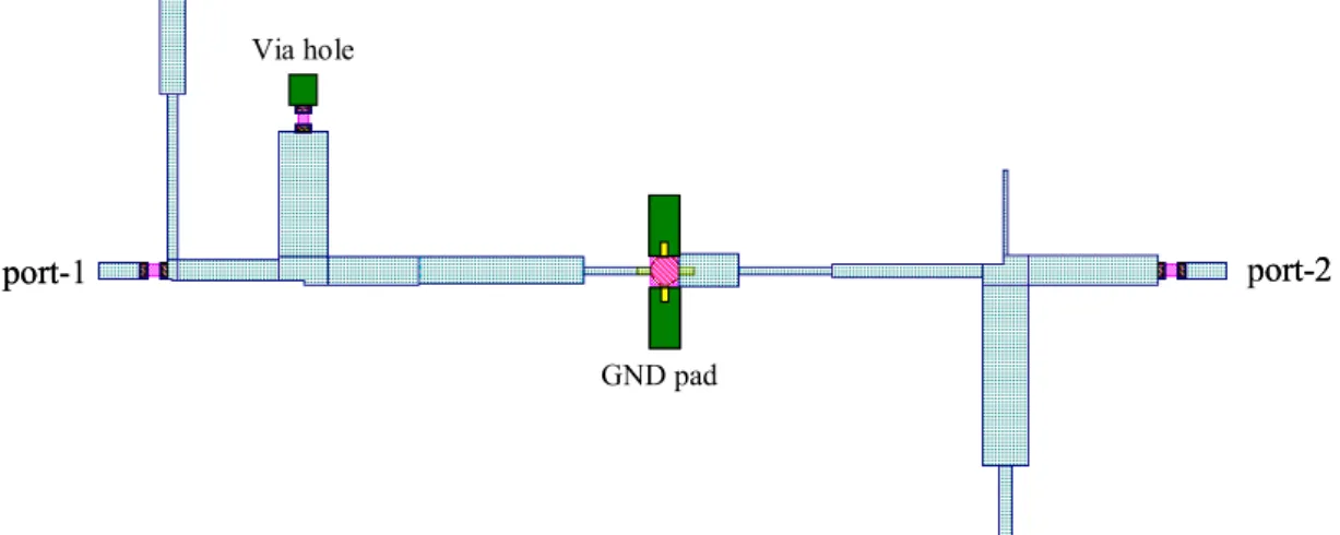
(56) Via hole. port-2. port-1 GND pad. Fig. 41 LNA circuit pattern. 46.
(57) Chapter 5 Conclusion We have introduced an evolutionary generation of microwave line-element circuits using GA. The developed procedure optimizes the line-element circuit within library and ends up with a circuit that accord with specifications. Some examples of specifications are tested to validate the procedure. GA’s are particularly effective to find optimal solutions in high dimensional parameter spaces and multi-object problems as they do not require derivations. Their robustness makes them a good choice for many synthesis tasks. Although the circuit pattern designed with traditional transmission-line、parallel open-stub、parallel stepped-impedance and parallel short-stub structure may cause a large circuit size, the same state appears in ref [5] and [29]. For having a compact circuit size, we can adopt hairpin-line、interdigital or cascaded trisection…, any elements which we can translate it into ABCD matrix form for narrow-band applications. When in the procedure of GA operator, crossover, there will be some actual circuit pattern make the restriction on. For example, in Fig.42, when crossover point is selected at gene-4, the portion of the chromosome preceding the selected point is copied from parent 1 to children 1 and from parent 2 to children 2. The portion of the chromosome of parent 1 following the selected point is placed in the corresponding positions in children 2 and vice versa for the remaining portion of the chromosome of parent 2. However, notice real circuit pattern crossover of children-1. There are all parallel stubs at gene-3、gene-4 in parent-1 and at gene-5、gene-6 at parent-2. When all parallel stubs are connected together, there are no circuit models available for the 47.
(58) six-branch discontinuities and it’s hard to fabricate it. We use a while-loop in crossover process, which will completely prevent this kind of phenomenon from taking place, but the while-loop may increase the GA computation time. For example, in chap 3.1, WLAN Dual-BPF applications, the GA computation time is about 1.5 hr with no constraint. If we combine the limiting conditions, the calculate time will be turned into 3 to 5 hours using Matlab.. parent-1 crossover point at gene-4 parent-2. children-1 how to connect?. children-2. Fig.42 Circuit pattern constraint in crossover process 48.
(59) Diligent direction in the future lies in combining discontinuous characteristics of microstrip-lines, which are step in width、open ends、gaps、bends and short ends. For the equivalent circuit modeling of these discontinuous characteristics, we can consult documents [24] [25] [26] [27]. To combine these equivalent circuits with GA program will satisfy the intact function of microwave circuit design. While we are analyzing the circuit specification that the method can’t be designed in general traditional methods, this thesis can offer another kind of thought and direction to design, and satisfy the characteristic demand of the circuit design.. 49.
(60) Reference [1] J. H. Holland, “Adaption in National and Artificial Systems,” University of Michigan Press, Ann Arbor, MI, 1975; MIT Press, Cambridge, MA, 1992. [2] Ming-Iu Lai and Shyh-Kang Jeng,“A Microstrip 3-Port and 4-Channel Multiplexer for WLAN and UWB coexistence,” accepted for publication in the IEEE Trans. Microwave and Technique and Theory. [3] T. Nishino and T. Itoh, “Evolutionary Generation of Microwave Line-Segment Circuits By Genetic Algorithms,” IEEE Transactions on Microwave Theory and Techniques, Vol.50, No.9, pp.2048-2055, September 2002. [4] J. M. Johnson and Y. Rahmat-Samii, “Genetic Algorithms in Engineering Electromagnetics,” IEEE Antennas and Propagation Magazine, Vol.39, No.4. pp.7-21, August 1997. [5] L. C. Tsai, C. W. Hsue, “Dual-Band Bandpass Filters Using Equal-Length Coupled-Serial-Shunted. Lines. and. Z-Transform. Techniques,”. IEEE. Transactions on Microwave Theory and Techniques,Vol.52,No.4,April 2004. [6] F. Liu and W. Lu and Q. Zheng, “An Improved Genetic Algorithms Optimizing Microstrip Filter With Equal Width,” IEEE Proceedings, Antennas, Propagation and EM Theory, pp.851-855, October 2003. [7] S. F. Peik and Y. L. Chow, “Genetic Algorithms Applied to Microwave Circuit Optimization,” Asia Pacific Microwave Conference, pp.857-860, 1997. [8] J. W. Bandler, R. M. Biernacki, S. H. Chen, D. G. Swanson and S. Ye, “Microstrip Filter Design Using Direct EM Field Simulation,” IEEE Transactions. on. Microwave. Theory. and. Techniques,. Vol.42,. No.7,. pp.1353-1359, July 1994. [9] D. S. Weile and E. Michielssen, “Genetic Algorithms Optimization Applied to 50.
(61) Electromagnetics: A Review,” IEEE Transaction on Antennas and Propagation, Vol.45, No.3, pp.343-353, 1997. [10] J. R. Koza, F. H. Bennett, D. Andre, M. A. Keane and F. Dunlap, “Automated Synthesis of Analog Electrical Circuits by Means of Genetic Programming,” IEEE Transaction on Evolutionary Computation, Vol.1, No.2, pp.109-128, 1997. [11] D. E. Goldberg, Genetic Algorithms in Search Optimization and Machine Learning, Addison-Wesley, 1989. [12] M. Gen and R. Cheng, Genetic Algorithms and Engineering Optimization, John Wiley & Sons, 2000. [13] Y. Rahmat-Samii and E. Michielssen, Electromagnetic Optimization by Genetic Algorithms, John Wiley & Sons, 1999. [14] D. E. Goldberg and K. Deb, A Comparative Analysis of Selection Schemes Used in Genetic Algorithms. In Foundations of Genetic Algorithms (G. J. E. Rawlins, ed.), pp.69-93. Morgan Kaufmann, San Mateo, CA, 1991. [15] M. Chu and D. J. Allstot, “Elitist Nondominated Sorting Genetic Algorithm Based RF IC Optimizer,” IEEE Transactions on Circuits and Systems-I: Regular Papers, Vol.52, No.3, March 2005. [16] J. W. Kim, S. W. Kim, P. G. Park and T. J. Park, “On the Similarities between Binary-Coded GA and Real-Coded GA in Wide Search Space,” CEC 2002 Proceedings, Evolutionary Computation, Vol.1, pp.681-686, May 2002. [17] D. M. Pozar, Microwave Engineering, 3 rd edition, John Wiley & Sons, 2005. [18] G. Gonzalez, Microwave Transistor Amplifiers: Analysis and Design, 2 nd edition, Prentice Hall, N. J., 1997. [19] K. Chang, ed., Handbook of Microwave and Optical Components, Vol.2, Wiley Interscience, N. Y., 1990. 51.
(62) [20] G. D. Vendelin, A. M. Pavio and U. L. Rohde, Microwave Circuit Design Using Linear and Nonlinear Techniques, Wiley, N. Y., 1990. [21] G. L. Mattaei, L. Young and E. M. T. Jones, Microwave Filters, Impedance -Matching Networks and Coupling Structures, Artech House, Dedham, Mass, 1980. [22] R. E. Collin, Foundations for Microwave Engineering, 2 nd edtion, McGraw-Hill, N. Y., 1995. [23] J. S. Wong, “Microstrip Tapped-Line Filter Design,” IEEE Transactions on Microwave Theory and Techniques, Vol.27, No.1, pp.44-50, 1979. [24] D. G. Swanson, “Grounding Microstrip Line with Via Holes,” IEEE Transcations on Microwave Theory and Technique, Vol.40, No.8, pp.1719-1721, August 1992. [25] M. E. Goldfarb and R. A. Pucel, “Modeling Via Hole Grounds in Microstrip,” IEEE Microwave and Guided Wave Letters, Vol.1, No.6, pp.135-137, June 1991. [26] T. C. Edwards and M. B. Steer, Foundations of Interconnet and Microstrip Design, 3 rd edition, John Wiley & Sons, 2000. [27] J.S.Hong and M.J.Lancaster, Microstrip Filters for RF/Microwave Applications, John Wiley & Sons, 2001. [28] J.Lee, M.S.Uhm and J.H.Park, “Synthesis of Self-Equalized Dual-Passband Filter,” IEEE Microwave and Wireless Components Letters, Vol.15, No.4, April 2005. [29] C.Quendo, E.Rius and C.Person, “An Original Topology of Dual-Band Filter with Transmission Zeros,” IEEE MTT-S International, Vol.1, pp.519-522, June 2003. [30] C.Quendo, E.Rius and C.Person, “Narrow Bandpass Filter Using Dual-Behavior 52.
(63) Resonators,” IEEE Transactions on Microwave Theory and Techniques, Vol.51, No.3, pp.734-743, March 2003. [31] C.Quendo, E.Rius and C.Person, “Narrow Bandpass Filter Using Dual-Behavior Resonators Based on Stepped-Impedance Stubs and Different-Length Stubs,” IEEE Transactions on Microwave Theory and Techniques, Vol.52, No.3, pp.1034-1044, March 2004. [32] “First Report and Order, Revision of Part 15 of Commission’s Rules Regarding Ultra-Wide Band Transmission Systems,” FCC, Washington DC, 2002. [33] T. Tong, “Preamplifier for Ultra-Wide Band System in 0.18µm CMOS Process, ” 5 th International Conference on ASIC Proceedings, Vol.2, pp.1078-1081, October 2003. [34] I. O’Donnell, M. Chen, S. Wang and B. Brodersen, “An Integrated, Low- Power, Ultra-Wideband Transceiver Architecture for Low-Rate Indoor Wireless Systems,” Presentation, University of California, Berkeley, September 2000. [35] R.Hu, “An 8-20GHz Wide-Band LNA Design and the Analysis of Its Input Matching Mechanism,” IEEE Microwave and Wireless Components Letters, Vol.14, No.11, November 2004. [36] B. Analui and A. Hajimiri, “Bandwidth Enhancement for Transimpedance Amplifiers,” IEEE Journal of Solid-State Circuits, Vol.39, No.8, August 2004. [37] A. John and R. H. Jansen, “Evolutionary Generation of (M)MIC Component Shapes Using 2.5D EM Simulation and Discrete Genetic Optimization,” IEEE MTT-S International, Microwave Symposium Digest, Vol.2, pp.745-748, June 1996. [38] Y. C. Chung and R. L. Haupt, “Gas using Varied & Fixed Binary Chromosome Lengths and Real Chromosomes for Low Sidelobe Spherical-Circular Array Pattern. Synthesis,”. IEEE. International 53. Symposium. on. Antennas. and.
(64) Propagation Society, Vol.2, pp.1030-1033, July 2000. [39] S. Chakravarty and R. Mittra, “Design of Microwave Filters Using a Binary Coded. Genetic. Algorithm,”. IEEE. Antennas. and. Propagation. Society,. International Symposium, Vol.1, pp.144-147, July 2000. [40] E. Michielssen, S. Ranjithan and R. Mittra, “Optimal multilayer filter design using real coded genetic algorithms,” IEE Proceedings-J, Vol.139, No.6, December 1992. [41] H. Ishida and K. Araki, “Design and Analysis of UWB Bandpass Filter with Ring Filter,” IEEE MTT-s International, Microwave Symposium Digest, Vol.3, pp.1307-1310, June 2004. [42] A. Saito, H. Harada and A. Nishikata, “Development of Bandpass Filter for Ultra Wideband (UWB) Communication Systems,” IEEE Conference on Ultra Wideband Systems and Technologies, pp.76-80, November 2003. [43] 郭仁財,微波工程,二版,高立圖書有限公司,民國九十年。 [44] 郭仁財,微波工程(一)課程講義,民國九十一年。 [45] 張志揚,微波工程(二)課程講義,民國九十二年。 [46] 周鵬程,遺傳演算法原理與應用—活用 Matlab,全華科技圖書有限公司,民 國九十年。 [47] 蘇木春,張孝德,機器學習:類神經網路、模糊系統及基因演算法則,全華 科技圖書有限公司,民國八十八年。 [48] 梁逢烈,基因演算法於以電磁場論為基礎之微波濾波器合成之應用,國立交 通大學電信工程研究所碩士論文,民國八十六年。 [49] 蔡世鵬,應用基因演算法於微波濾波器之最佳化設計,國立交通大學工業工 程研究所碩士論文,民國八十五年。. 54.
(65)
數據
相關文件
路徑 I 是考慮空氣的阻擋效應所算出的運動路徑。球在真 空中的運動路徑 II 是以本章的方法計算出的。參考表 4-1 中的資料。 (取材自“ The Trajectory of a Fly Ball, ” by
雙極性接面電晶體(bipolar junction transistor, BJT) 場效電晶體(field effect transistor, FET).
(二)計算方式:雇主繼續僱用於前款計算期間內,預估成就勞動基準
微算機原理與應用 第6
計算機網路 微積分上 微積分下
應用閉合電路原理解決生活問題 (常識) 應用設計循環進行設計及改良作品 (常識) 以小數加法及乘法計算成本 (數學).
請繪出交流三相感應電動機AC 220V 15HP,額定電流為40安,正逆轉兼Y-△啟動控制電路之主
4.2 Copy the selected individuals, then apply genetic operators (crossover and mutation) to them to produce new individuals.. 4.3 Select other individuals at random and
