國 立 交 通 大 學
電子工程學系 電子研究所碩士班
碩 士 論 文
氟應用於二氧化鉿儲存層
非揮發性記憶體之研究
Study on Fluorine Applied to Nonvolatile Memory
Using HfO
2as Charge Trapping Layer
研 究 生:林文新
指導教授:羅正忠 博士
氟應用於二氧化鉿儲存層
非揮發性記憶體之研究
Study on Fluorine Applied to Nonvolatile Memory
Using HfO
2as Charge Trapping Layer
研 究 生:林文新 Postgraduate:Wen-Shin Lin
指導教授:羅正忠 博士 Advisor:Dr. Jen-Chung Lou
國 立 交 通 大 學
電子工程學系 電子研究所碩士班
碩 士 論 文
A Thesis
Submitted to Department of Electronics Engineering & Institute of Electronics Engineering and Computer Science
National Chiao-Tung University in Partial Fulfillment of the Requirements
for the Degree of Master in
Electronics Engineering June 2010
Hsinchu, Taiwan, Republic of China
-i- 摘要
氟應用於二氧化鉿儲存層非揮發性記憶體之研究
研究生:林文新 指導教授:羅正忠 博士 國立交通大學 電子工程學系 電子研究所碩士班摘要
為了節省晶圓成本,增加產率,降低操作電壓,所製作的元件尺 寸不斷微縮,其中非揮發性記憶體(NVM)也是如此,高密度記憶單元、 低功率消耗、快速讀寫操作、以及良好的可靠(Reliability),又是 在微縮之下的目標與方向。其中可靠度的改善一直是許多論文所研究 的議題,以資料保存時間(Retention)和耐操度(Endurance)的改良為 主要方向。 本篇論文中,閘極採用乾氧成長二氧化矽(dry SiO2)作為穿隧氧化層(tunnel oxide),其中以二氧化鉿取代傳統的 SONOS 結構的氮化
矽(Si3N4)作為儲存層,並在沉積完二氧化鉿後,進行四氟化碳電漿
-ii- 由四乙氧基矽烷(TEOS)組成的二氧化矽作為阻擋氧化層(blocking oxide)。雖然二氧化鉿寫入時比氮化矽擁有較大的記憶窗口(window) ,但二氧化鉿在資料保存時間上的表現是遜色於氮化矽的。為了改善 資料保存時間,我們進行四氟化碳電漿處理,將氟的擴散進入二氧化 鉿,氟與鉿鍵結形成 Hf-F,因此二氧化鉿儲存層中低能階的陷阱被 修補,而高能階陷阱仍留下,減少記憶體在寫入後儲存電荷逃逸漏電 之現象,進而得到較佳的資料保存時間。 我們將會電容和 SOHOS 記憶體元件作基本電性量測,藉此獲取資 料保存時間趨勢。在材料分析方面,也使用 X 光光電子能譜術(XPS), 分析將氟擴散的電漿處理前後,是否形成鉿與氟鍵結情形;使用二次 離子質譜儀(SIMS)分析顯示氟所分佈的位置。 根據實驗結果,確實驗證四氟化碳電漿處理,確實地改善了以二 氧化鉿作為儲存層的非揮發性記憶體,在資料保存時間上的不足,此 外,在製程中加上四氟化碳電漿處理,合用於傳統 SONOS 記憶體製程, 並且屬於較低溫的製程,不會增加過多二氧化鉿形成結晶的負擔,因 此我們認為這樣的製程技術對未來的記憶體元件是可以期待與考慮 使用的
-iii-
ABSTRACT
Study on Fluorine Applied to Nonvolatile Memory
Using HfO
2as Charge Trapping Layer
Student:Wen-Shin Lin Advisor:Dr. Jen-Chung Lou Department of Electronics Engineering & Institute of Electronics
College of Electrical and Computer Engineering National Chiao-Tung University
Abstract
In order to save the cost, increase the throughput and decrease operation voltage, many kinds of the devices are continually scaling. Undoubtedly, the nonvolatile memory (NVM) device is one of the scaling devices. Moreover, Current requirements of nonvolatile memory are the high density cells, low-power consumption, high-speed operation and good reliability for the scaling down devices. There are many studies that discuss how to improve the reliability including retention and endurance. In this study, silicon oxide (SiO2) is grown for tunnel oxide layer. The
trapping layer of traditional SONOS structure is silicon nitride (Si3N4)
which is replaced with hafnium oxide (HfO2). After HfO2 is deposited,
we proceed to CF4 plasma treatment. Then, SiO2, composed of
tetraethoxy silane (TEOS), is deposited as blocking oxide. While the memory window of HfO2 is larger than Si3N4, the retention performance
-iv-
of HfO2 is worse than Si3N4. In order to improve the retention
performance, we use CF4 plasma treatment to diffuse fluorine into HfO2
after HfO2 is deposited. The fluorine is incorporated into the HfO2
trapping layer and then formed of Hf-F bonding with hafnium. Because of CF4 plasma treatment, the shallow traps would be recovered but the
deep traps would still be left. The carriers’ de-trapping effect is decreased after program operation. Hence, the retention performance would be better.
We probe into the electrical characteristics of the capacitors and the SOHOS memory devices. From fundamental electric characteristic data, we could know retention information. In materials analysis, X-ray photoelectron spectroscopy (XPS) is used to analyze the devices which were carried out CF4 plasma treatment and confirm if there is the Hf-F
bonding. Besides, the secondary ion mass spectroscopy (SIMS) analyses show depth profiles of fluorine in the devices.
According to the experiment results, the retention performance of NVM, carried out CF4 plasma treatment, is actually improved. Moreover,
CF4 plasma treatment is compatible with the conventional SONOS
memory process. It is also the low thermal budget process which would not make the HfO2 film more crystallized. Therefore, we all consider the
process technology is potential and expectable gradually for the memory device in the future.
-v-
誌謝
感謝交通大學提供實驗環境資源予我們,兩年來學習相當多的東 西,不管是學業上還是生活上,同時讓我擁有了珍貴回憶,未來我也 以交大為榮,也希望能讓交大以我為榮,也一定要感謝我的指導教授, 羅正忠教授,對我的照顧與指導,並且在IC技術這門課上認真的教學, 更是讓所有電子所的學生能夠精確地掌握製程技術的關鍵,不僅讓我 在實驗上更加順利也豐富我的知識。此外,智仁學長更可以說是我的 第二位指導教授了,感謝對我的照顧,也在實驗論文上,給予最大的 幫助,讓我清楚研究方向也豐富我的知識。感謝威良學長在學業上不 斷的支援我們,有問必答,且不厭其煩。也謝謝翊賞和哲輔學長的幫 助讓我們在機台上更熟練,也幫助我們更快認識碩士生活,芳毓和尚 勳感謝你們的照顧,我很榮幸與你們成為好朋友好夥伴一起為實驗研 究打拚。謝謝電子所的學長與同學,不少人不吝嗇的協助過我,讓我 感到電子所的溫暖,電子所的老師們,總是認真的教學毫不保留的將 功力傳授予我們,我們很幸福,謝謝老師們。 最後我要將我的這份榮耀和喜悅獻給我最尊敬的父親張平賢先 生、母親林聖美女士,還有很疼我的兩位哥哥張文德、張文彬,謝謝 你們不留餘力的關心與照顧。要感謝的人太多,在此向大家致上最深 的敬意,祝福大家都健康平安、事事順心。-vi-
Contents
Chinese Abstract………ⅰ English Abstract……….ⅲ Acknowledgment (Chinese)…...………ⅴ Content………ⅵ Table Captions……...……….………ⅷ Figure Captions………..ⅸ Chapter.1 Introduction 1.1 General Background---1 1.2 Motivation---101.3 Organization of This Thesis---12
Chapter.2 Basic Principles of Nonvolatile Memory 2.1 Program/Erase Operation Mechanisms---19
2.2 Reliability of Nonvolatile Memory---25
2.3 High-k Material as Trapping Layer---28
Chapter.3 Device Fabrication and Characterization 3.1 Introduction---36
3.2 Experimental Procedures---37
3.3 Results and Discussions---40
-vii-
Chapter.4 Conclusion and Suggestion for Future Work
4.1 Conclusion---63 4.2 Suggestions of the Future Work---64 *Reference---65
-viii-
Table Captions
Chapter1
Table 1.1 Performance Comparison between volatile memory (DRAM and SRAM) and nonvolatile memory (Flash, FRAM, MRAM and Phase Change Memory) devices. Among the nonvolatile memories, Flash memory is the only memory compatible with the current CMOS process flow. Overall, the Flash memory exhibits the best performance except for the disadvantages of high programming voltage and slow program/erase speed.
Chapter2
Table 2.1 Trapping material properties
Chapter3
Table 3.1 The split table of capacitors.
-ix-
Figure Captions
Chapter1
Fig1-1: Schematic cross section of the conventional floating gate nonvolatile memory device. Poly-Si floating gate is used as the charge storage element
Fig1-2: Schematic cross section of ETOX device
Fig1-3: I-V curves of a floating gate device when there is no charge stored in the FG (“1”-curve) and when a negative charge Q is stored in the FG (“0”-curve)
Fig1-4: The structure of the nanocrystal nonvolatile memory device. The semiconductor nanocrystals or metal nanocrystals are used as the charge storage element instead of the continuous poly-Si floating gate.
Fig1-5: The development of the gate stacks of SONOS EEPROM memory devices. The optimization of nitride and oxide films has been the main focus in recent years.
Fig1-6: The structure of the SONOS nonvolatile memory device. The nitride layer is used as the charge-trapping element.
Fig1-7: Energy band diagrams of SONOS Flash memory. Large ϕ0 will block electron leakage effectively and improve retention time.
Chapter2
Fig2-1: The procedure of channel hot electrons injection (CHEI). Fig2-2: The approach of FN programming method, when
Eox > Φ1 XOT
-x-
Fig2-3: The approach of MFN programming method, when Φ1−Φ2
XOT > EOT >
Φ1−Φ2 XOT + (εεOX
N )XN
Fig2-4: The approach of TAT programming method, when Φ3 XOT > EOT > Φ3 XOT + (εεOX N )XN , Φ3 = Φ1 − Φ2−Φt
Fig2-5: Band diagram of a MOS structure along the vertical direction through the depletion region illustrating band-to-band and trap-to-band tunneling mechanisms.
Fig2-6: The procedure of band to band hot electron injection. Fig2-7: The procedure of band to band hot holes injection.
Fig2-8: Bandgap diagram of a SONOS device in the excess electron state, showing retention loss mechanisms: trap-to band tunneling (T-B), trap-to-trap tunneling (T-T), band-to-trap tunneling (B-T), thermal excitation (TE) and Pool-Frenkel emission (PF).
Fig2-9: Ideal energy band diagrams for (a) SONOS and (b) SOHOS structures.
Fig2-10: Energy band diagram schematic of the SONOS structure with HfO2 (solid lines) or Si3N4 (dashed lines) as the charge storage
layer during write (program) operations.
Chapter3
Fig 3-1(a): Schematic cross section of the HfO2 capacitors.
Fig 3-1(b): Process flows for fabricating various HfO2 capacitors.
Fig 3-2(a): Schematic cross section of the HfO2 SOHOS device.
-xi-
Fig 3-3: SIMS profile of capacitors with CF4 plasma treatment
Fig 3-4(a): The C-V hysteresis curve of capacitors with RTA and CF4
plasma treatment after bidirectional sweeps
Fig 3-4(b): The memory window characteristic of capacitors with RTA treatment
Fig 3-4(c): The memory window characteristic of capacitors with CF4
plasma treatment
Fig 3-4(d): The comparisons of the memory window characteristic for RTA and CF4 plasma treatment capacitor
Fig 3-5: The XRD spectra of crystallized HfO2 with RTA and CF4 plasma
treatment
Fig 3-6: The comparisons of the gate leakage current-voltage (IG-V)
characteristics for RTA and CF4plasma treatment capacitors
Fig 3-7(a): The retention characteristics of capacitors with RTA treatment at room temperature
Fig 3-7(b): The retention characteristics of capacitors with CF4 plasma
treatment at room temperature
Fig 3-7(c): The comparisons of the retention characteristic for RTA and CF4 plasma treatment capacitors
Fig 3-8: The XPS spectra for Hf 4f core levels from HfO2 with RTA and
CF4 plasma treatment
Fig 3-9: The comparisons of the surface roughness for HfO2 with RTA
and CF4 plasma treatment by AFM
Fig 3-10: The comparisons of the thickness for HfO2 with RTA and CF4
plasma treatment
-xii-
Oxygen vacancy is defined as OV in the figure Fig 3-12(a): The IDS-VDS curves of HfO2 SOHOS device
Fig 3-12(b): The IDS-VGS curves of HfO2 SOHOS device
Fig 3-13(a): Program characteristics of P40 with different operating condition
Fig 3-13(b): Erase characteristics of P40 with different operating condition
Fig 3-14(a): Program characteristics of P50 with different operating condition
Fig 3-14(b): Erase characteristics of P50 with different operating condition
Fig 3-15(a): Program characteristics of Control with different operating condition
Fig 3-15(b): Erase characteristics of Control with different operating condition
Fig 3-16: The comparisons of the retention characteristic for Control and CF4 plasma treatment devices at room temperature
Fig 3-17: The comparisons of the retention characteristic for Control and P50 at different temperatures
Fig 3-18: The comparisons of the retention characteristic for Control and CF4 plasma treatment devices at room temperature after 10
4
cycles
Fig 3-19: The comparisons of the endurance characteristic for Control and CF4 plasma treatment devices
- 1 -
CHAPTER 1
Introduction
1.1 General Background
In modern times, the application of Flash memory is indispensable. Flash memory not only has wide and practical applications extremely but also is considered as a technology driver for semiconductor industry in the next decade. It can be classified into two major applications: code storage application and data storage application. NOR type Flash memory is the most suitable for code storage application, such as DVD player, PC bios, and cellular phones; NAND type Flash memory has been targeted at data storage application, such as USB flash personal disc, memory cards, MP3 audio players, digital cameras, and PDA. In short, the 3C products are almost based on Flash memory.
Flash memory is a kind of nonvolatile memory that can keep stored information even though the power supply is switched off. It also has exhibited several advantages, like the ability to be electrical programmed and fast simultaneously block electrical erased in a single-cell, the smallest cell size to own the highest chip density, and the good flexibility. Furthermore, the fabrication process of Flash memory is compatible with the current CMOS process and is a suitable solution for embedded memory applications. Therefore, Flash memory is easily a scalable replacement for Erasable Programmable Read Only Memory (EPROM) and Electrically Erasable Programmable Read Only Memory (EEPROM). We will compare Flash memory with other nonvolatile memories later.
- 2 -
Since the first MOSFET device was invented by Ligenza and Spitzer in 1960, one of the most revolutionary technology drivers to settle the direction of the development of semiconductor industries is the semiconductor memory. Magnetic-core memory is the large volume, high cost, and high power consumption so that the electronic industries urgently needed new species of memory devices to replace the magnetic-core memory. For this reason, D. Kahng and S. M. Sze invented the first floating-gate (FG) nonvolatile semiconductor memory at Bell Labs [1] in 1967. To date, the stacked-gate floating gate device structure, as shown in Fig. 1-1, has been the most prevailing nonvolatile-memory implementation, and has used widely in both standalone and embedded memories. The invention of FG memory not only affects to replace magnetic-core memory but also creates a monumental industry of portable electronic systems. Flash memory is the most wide spread FG memory array organization, and it has a byte-selectable write operation combined with a sector “flash” erase.
In the past decade, the booming market of portable electronic devices such as digital cameras and cellular phones makes memory chips with low power consumption and low cost get more and more attention. These applications want the memory to have ten years data retention time; hence, the nonvolatile memory (NVM) device has become indispensable. There are four major types of nonvolatile memory technology: Flash memory, Ferro-electric Random Access Memory (FeRAM), Magnetic Random Access Memory (MRAM) and Phase Change Memory (PCM).
- 3 -
most suitable option for the following reasons:
(1) Flash memory can accomplish the highest chip density, as a Flash memory cell consists of only one transistor [2]. A MRAM cell needs a transistor and a magnetic tunnel junction [4], while a FeRAM memory cell generally comprises one transistor and one capacitor [3]. PCM was considered as a promising nonvolatile memory [5], but its memory cell consists of one resistor and a bipolar junction transistor. Until now, only a 256MB PCM chip has been developed. It needs taking more effort to develop if PCM is really a promising technology.
(2)FeRAM is not an idea nonvolatile memory because its reading mode is a destructive type of operation. A programming verification is required to restore the data after reading. On opposite sides, Flash memory doesn’t need the additional action. In other words, the reading operation of Flash memory is not destructive, and it affects slighter data retention disturbance than FeRAM.
(3) The fabrication process of Flash memory is compatible with the current CMOS process and is a suitable solution for embedded memory applications. A Flash memory cell is similar to a MOSFET cell, except that a poly-silicon floating gate [9] (or Silicon Nitride charge trapping layer [8]) is placed in between a tunnel oxide and an inter-poly oxide to form a charge storage layer. All other nonvolatile memories require integration of new materials that are not compatible with a conventional CMOS process. Therefore, it is easier and more reliable to integrate Flash memory than other nonvolatile memories with logic and analog devices to achieve better chip performance for wireless computation and wireless communication [10].
- 4 -
(4) Four distinct threshold voltage (Vth) states can be achieved in a Flash
memory cell by trapping the number of charges in the charge storage layer. Hence, Flash memory can possess the multi-bit per cell storage property [6]. Two-bits/cell (with four Vth states) Flash memory cells have already been
commercialized; four-bits/cell Flash memory device is feasible and is under development now [7]. Multi-bit storage increases memory density and reduces the cost per bit significantly. In addition, Matrix Semiconductor Inc. demonstrated multi-layer SONOS Flash memory [8]. This novel structure makes another possibility to achieve even higher density and lower cost technologies based on Flash memory. On account of these critical advantages, Flash memory has turned into the chief nonvolatile memory device in this generation.
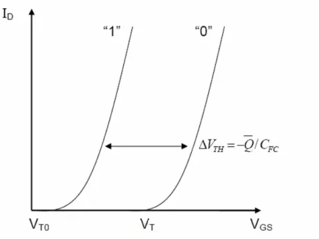
The Flash memory cell structure was invented originally by D. Kahng and S. M. Sze in 1967, and Intel ETOX (EPROM Tunnel Oxide) structure, shown in Fig. 1-2 , is the famously commercial Flash memory in 1988 [11]. The operation principal is using the poly-silicon which is above the tunnel oxide layer and named Floating Gate as the charge store unit for the device. ETOX could be programmed or erased by Channel-Hot-Electron-Injection (CHEI), Fowler-Nordheim tunneling (F-N), or Band-to-Band-Hot-Hole (BTBHH). The threshold voltage of Flash memory will be shifted after electrons are injected into the FG from the channel. Therefore, the logical “0”and “1” of nonvolatile memory devices can be defined by the different states of the threshold voltage (Fig. 1-3). The specification of the concept will be described in Chapter 2.
Even though conventional FG devices achieve a great commercial success, there are some limitations. Two of the most dominant limitations are: (1) the
- 5 -
potential for continued scaling down of the device structure. This scaling down limitation results from the tunnel oxide layer. The tunnel oxide should be thin enough so that carriers can transport to and from the floating gate quickly and efficiently. On the other hand, the tunnel oxide also is required to supply well isolation to retain information integrity over periods of up to a decade under retention, endurance, and disturbed conditions. If the tunnel oxide is thinner for the faster operation speed consideration, characteristics of the retention will be degraded. On the contrary, if the tunnel oxide is thicker for the superior isolation account, the operation speed will be slower. There is a trade-off between the operation speed and the reliability. Hence, we need to find the proper tunnel oxide thickness for the better product functions. (2) As plenty of program/erase cycles, the strength and quality of tunnel oxide will degrade. Once a leaky path is created in the tunnel oxide, all the charges stored in the floating gate will be lost.
Two suggestions, Poly-Silicon/Oxide/Nitride/Oxide/Silicon (SONOS) [12-14] and nanocrystal nonvolatile memory devices [15-17], have been demonstrated to lead to an improvement in retention time and endurance compared with conventional floating gate memory. Hence, the tunnel oxide thickness can be reduced to allow faster program speed and lower operation voltage.
1.1.1 Nanocrystal Nonvolatile Memory Devices
Nanostructure nonvolatile memory is introduced in the early 1990s firstly. IBM researchers proposed flash memory with a granular floating gate made of silicon nanocrystals [73]. The term “nanocrystal” refers to a crystalline structure
- 6 -
with a nanoscale dimension and its electronic properties seem more similar to an atom or molecule rather than the bulk crystal. Fig. 1-4 illustrates conventional nanocrystal nonvolatile memory (NVM) device structure. It could be found that the nanocrystals are separated by the isolation within the gate dielectric. For a nanocrystal NVM device, the charge storage media is in the form of mutually isolated nanocrystals rather than the continuous poly-silicon layer. The limited size and capacitance of nanocrystals limit the numbers of stored electrons; collectively the stored charges screen the gate charge and control the channel conductivity of the memory transistor.
Nanocrystal-based NVM devices have recently attracted much attention in consequence of their potential to overcome the limitations of conventional poly-silicon-based flash memory. There are several advantages of using nanocrystals as charge storage media. The main one is the potential to use thinner tunnel oxide without sacrificing retention. This is an entirely attractive proposition since reducing the tunnel oxide thickness is a key to lowering operation voltage and increasing operation speed. The claim of improving scalability results from the local charge storage in discrete nodes, which make the storage more fault-tolerant and immune to the leakage current caused by localized oxide defects. In addition, the lateral charge migration effect between nanocrystal can be diminished by the strongly isolation of surrounded dielectric. There are other important advantages. First, nanocrystal memory uses the more simplified fabrication process as is compared to conventional stacked-gate FG NVM’s avoiding the fabrication complications and costs of a dual-poly process. Second, due to the absence of drain to FG coupling, nanocrystal memory suffers
- 7 -
the less from drain-induced-barrier-lower (DIBL) so that it has the better suppressing punch through characteristic. One way to utilize this advantage is using a higher drain bias during the read operation, thus reducing memory access time [74]. Furthermore, it allows the use of shorter channel length and therefore higher cell density. Finally, nanocrystal memory owns excellent immunity to stress induced leakage current (SILC) and oxide defects on account of the discrete charge storage nodes in the nanocrystal layer.
Research in this structure has focused on the development of fabrication processes and nanocrystal materials, and on the integration of nanocrystal-based storage layers in actual memory devices.
1.1.2 SONOS Nonvolatile Memory Devices
The originally nitride-base device is metal-gate nitride device Metal/Nitride/Oxide/Silicon (MNOS) which was introduced in 1967 by Wegener et al [65]. Silicon nitride film contains many carrier traps which could trap carriers and cause threshold voltage shift. Then the silicon nitride trap-based devices are extensively studied for charge storage device application in the early 70s. Fig. 1-5 illustrates the progression of device structure, which has led to the present poly-Silicon-Oxide-Nitride-Oxide-Silicon (SONOS) device structure. In the early 1970s, the initial device structure was p-channel MNOS structure with aluminum gate electrode and thick (45 nm) silicon nitride charge storage layer. Program/erase voltages were about 25-30 V. In the late 1970s and early 1980s, the device structure developed to n-channel SNOS device with program/erase voltages of 14-18 V. In the late 1980s and early 1990s, n- and p-channel
- 8 -
SONOS devices emerged with program/erase voltages of 5-12 V. The advantages of the ONO triple dielectric layer are: (1) that charge injection from and to the gate electrode is minimized for both gate polarities, particularly for hole injection; (2) lower program voltage since the blocking action of the top oxide removes any limitation on reducing the nitride thickness; (3) improving memory retention since there is minimal loss of charge to the gate electrode.
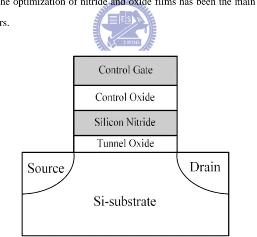
The SONOS memory device, shown in Fig. 1-6, has received much attention due to its advantages over the traditional floating-gate flash devices. These include reducing process complexity, higher operation speed, lower operation voltage, improving cycling endurance, and elimination of drain-induced turn-on [66-68]. The significant difference between floating-gate and SONOS structure is the way of charge storage. The charge storage media is the conductive poly-silicon floating-gate electrode. In the SONOS memory structure, charges are stored in the physical discrete traps of silicon nitride dielectric layer. A typical trap has a density of the order 1018-1019 cm-3 according to Yang et al [69] and stores both holes and electrons injected from the channel. The charges cannot move freely between the discrete trap locations so that the SONOS memory device is very hardy against the defects inside the tunnel oxide and has good endurance.
The SONOS memory device still encounters challenges in the future for high density nonvolatile memory application, which requires low voltage (< 5V), low power consumption, excellent retention, and superior endurance. Various methods have been proposed for improving the SONOS performance and reliability. For instance, Chen et al. demonstrated a Si3N4 band-gap engineering
- 9 -
(BE) control method for better endurance and retention. A nitride with varied relative Si/N ratio throughout the film has increased the charge-trapping efficiency significantly [70]. Besides, Tan et al. proposed that over-erase phenomenon in SONOS memory structure can be minimized by replacing silicon nitride with HfO2 as the charge storage layer. HfAlO composed of 10%
Al2O3 and 90% HfO2 improves the charge retention and endurance, while it
maintains the over-erase resistance of HfO2 [71]. She et al. showed that
high-quality nitride is applied as the tunnel dielectric layer for a SONOS-type memory device. Compared with SiO2 as tunnel dielectric layer, faster program
speed and better retention time are achieved with low operation voltage [72]. Lee et al. demonstrated a device structure of SiO2/Si3N4/Al2O3 (SANOS) with
TaN metal gate. TaN metal gate is more effective than a traditional poly-silicon gate to obstruct electron current through Al2O3 layer, resulting in faster
program/erase speed and significantly decreasing the saturation level of the erase threshold voltage [73].
Chen et al. researched a polycrystalline silicon thin-film transistor (poly-Si TFT) with oxide/nitride/oxide (ONO) gate dielectric layers and multiple nanowire channels for the applications of both SONOS memory and switch transistor [75]. The proposed NW SONOS-TFT exhibits superior memory device characteristics with high program/erase efficiency and stable retention at high temperature. Such a SONOS-TFT is thereby highly promising for applications of system-on-panel display in the future.
New device structures are also indispensable in making flash memory more scalable, since SONOS flash memory offers a thinner gate stack than floating
- 10 -
gate flash memory and a Fin-FET structure controls the short channel effect much better than a bulk structure. It has been demonstrated that the Fin-FET SONOS flash memory device with a much smaller cell size can achieve both remarkable performance and reliability. Hence, Fin-FET SONOS memory has potential to become the candidate for the next generation flash memory [76-77]. In past decade, about 20% of semiconductor market is given by the semiconductor memory, and the output value of Flash memory is expected to reach US$ 60 billion in 2010. The Development of the higher capacity and faster Flash nonvolatile memory is always one of the most important issues for technologic applications. In order to arrive at the goal, downsizing or multi-bit is the key point for pushing next generation development. In addition, the most important performance of Flash memory is reliability characteristic, such as program/erase cycling and data retention. It is well known that the tunnel oxide degradation during Fowler-Nordheim (FN) stress results from the oxide trap and interface trap generation. In conclusion, how to improve the reliability of Flash memory is the emphasis in this study.
1.2 Motivation
According to the International Technology Roadmap for Semiconductors (ITRS) [20], high-k dielectric materials would be able to maintain an equivalent potential difference from the floating gate to the device body for a larger thickness compared to SiO2. Hence, the charge leakage of the trapping layer can
be diminished so that the scaling limits will be extended.
- 11 -
(called SOHOS, Poly-Silicon/Silicon-Oxide/High-k/Silicon-Oxide/Silicon), such as high program/erase speed, easy to fabricate, low power consumption and low program voltage, better potential for scalability below the 70-nm node. Hafnium oxide (HfO2) is considered to replace the Si3N4 trapping layer of
SONOS-type Flash memory [21]. Furthermore, HfO2 is expected to have better
charge trapping characteristics than the traditional Si3N4 film. SOHOS can
achieve longer retention time than SONOS due to the density of trap state and deep trap energy level [22-24].
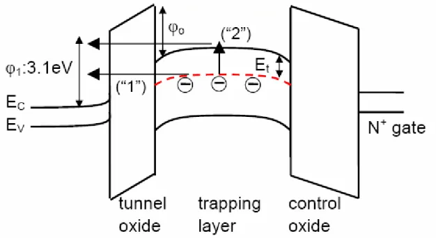
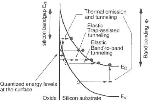
Although SONOS Flash memory device has attracted lots of attention due to its advantages over the traditional floating-gate Flash memory device, it still faces challenges for further improvement. For instance, the tunnel oxide thickness cannot be reduced below 25Å in order to improve the program speed, if 10-years retention time must be guaranteed [25]. As shown in Fig. 1-7, there are two charge-loss mechanisms: (1) direct tunneling, with an associated barrier height φ o+Et ; and (2) thermally assisted de-trapping into the nitride conduction band and subsequent tunneling through the tunnel oxide, with associated barrier height φo. A high conduction band offset φo between the trapping layer and the tunnel oxide is essential for the better retention. The band offset φo for a nitride trapping layer is only 1.05 eV and the offset φo for HfO2 trapping layer is up to 1.6 eV. Therefore, we use the HfO2 film as the
trapping layer rather than Si3N4 film in this research.
However, the retention performance of HfO2 is worse than Si3N4 actually due
to a lot of defects inside HfO2. The defects become the traps, which also include
- 12 -
that memory window will be decrease rapidly. In other words, the retention performance will be degraded. In addition, the poor retention performance of HfO2 can be attributed to the presence of conduction paths in the high-k material.
After post deposit annealing, the HfO2 film is crystallized. For those reasons,
Si3N4 SONOS-type structures show the significantly better retention
performance than HfO2 SONOS-type structures. If we want to use HfO2 as
storage layer, we should overcome those issues.
In this study, fluorine incorporation into the HfO2 trapping layer by post CF4
plasma treatment is proposed to improve the retention performance. The fluorine is incorporated into the HfO2 trapping layer and then formed of Hf-F bonding
with hafnium. Because of CF4 plasma treatment, the shallow traps would be
recovered by the fluorine, but the deep traps would still be left. Furthermore, the process of CF4 plasma treatment is compatible with the conventional SONOS
memory process. It is also the low temperature process which would not increase the crystals of the HfO2 film. Those make the retention performance
become better.
By post CF4 plasma treatment, we expect to advance the reliabilities of the
Flash memories. Hence, we consider that the process technology is potential and expectable gradually in the future.
1.3 Organization of This Thesis
In Chapter 1, the potential memory devices about nonvolatile memory
(NVM), conventional Flash SONOS and SOHOS devices are introduced in this chapter.
- 13 -
In Chapter 2, basic principle of nonvolatile memory is introduced. In Chapter 3, the device characteristics will be discussed
In Chapter 4, Materials Analysis
In Chapter 5, this section includes the conclusions and the future work of this
- 14 -
Table 1.1: Performance Comparison is between volatile memory (DRAM and SRAM) and nonvolatile memory (Flash, FRAM, MRAM and phase change memory) devices. Among the nonvolatile memories, Flash memory is the only memory compatible with the current CMOS process flow. Overall, the Flash memory exhibits the best performance except for the disadvantages of high programming voltage and slow program/erase speed.
- 15 -
Fig 1-1: Schematic cross section of the conventional floating gate nonvolatile memory device. Poly-Si floating gate is used as the charge storage element
- 16 -
Fig 1-3: I-V curves of a floating gate device when there is no charge stored in the FG (“1”-curve) and when a negative charge Q is stored in the FG (“0”-curve).
Fig 1-4: The structure of the nanocrystal nonvolatile memory device. The semiconductor nanocrystals or metal nanocrystals are used as the charge storage element instead of the continuous poly-Si floating gate.
- 17 -
Fig 1-5: The development of the gate stack of SONOS EEPROM memory devices. The optimization of nitride and oxide films has been the main focus in recent years.
Fig 1-6: The structure of the SONOS nonvolatile memory device. The nitride layer is used as the charge-trapping element.
- 18 -
Fig 1-7: Energy band diagrams of SONOS Flash memory. Large ϕ0 will block electron leakage effectively and improve retention time.
- 19 -
CHAPTER 2
Basic Principles of Nonvolatile Memory
2.1 Program/Erase Operation Mechanisms
Most of operations on novel nonvolatile memories, such as nanocrystal and SONOS memories are base on the concept of Flash memory. If charge has to be stored in a bit of the memory, there are some different procedures. The threshold voltage shift of a Flash memory transistor can be written as [31-32]:
∆𝑉𝑇𝐻 = −𝐶𝑄
𝐹𝐶… … 𝑒𝑞. 2 − 1
Where Q is a negative charge stored in the FG, and FC C is the capacitances between the floating gate (FG) and control gate. The threshold voltage of the memory cell can be altered by changing the amount of charge present between the gate and the channel, corresponding to the two states of the memory cell, i.e., the binary values (“1” and “0”) of the stored bit. Figure 1-3 shows the threshold voltage shift between two states in a Flash memory. Regarding a nonvolatile memory, it can be “written” into either state “1” or “0” by either “programming” or “erasing” operation, which are decided by the definition of memory cell itself. There are many solutions to achieve “programming” or “erasing”. In general, hot carrier electron injection (HCEI) F-N tunneling and band to band tunneling (BTBT), are three kinds of common operation mechanism employed in novel nonvolatile memories. The three mechanisms will lead difference characteristics for nonvolatile memories.
- 20 -
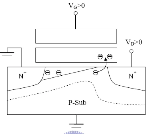
2.1.1 Channel Hot-Electron Injection (CHEI)
The physical mechanism of CHEI is relatively simple to understand qualitatively. An electron traveling from the source to the drain gains energy from the lateral electric field and loses energy to the lattice vibrations (acoustic and optical phonons). At low fields, this is a dynamic equilibrium condition, which holds until the field strength reaches approximately 100kV/cm [33]. For fields exceeding this value, electrons are no longer in equilibrium with the lattice, and their energy relative to the conduction band edge begins to increase. Electrons are “heated” by the high lateral electric field, and a small fraction of them have enough energy to surmount the barrier between oxide and silicon conduction band edges. Figure 2-1 shows schematic representation of CHEI MOSFET and the energy-distribution function with different fields. On the other hand, the effective mass of hole is heavier than one of electron. It is too hard to obtain enough energy to surmount oxide barrier. Therefore, hot-hole injection rarely is employed in nonvolatile memory operation. For an electron to overcome this potential barrier, three conditions must hold [34].
(1) Its kinetic energy has to be higher than the potential barrier. (2) It must be directed toward the barrier.
(3)The field in the oxide should be collecting it.
During programming, the positive voltages applied to the gate and drain while the source is grounded. These voltages generate a lateral and vertical electric field along the channel. The electrons will move from the source to the drain and be accelerated by high lateral field near the drain junction in the channel. Once the electrons gain enough energy, they can surpass the energy barrier of the
- 21 -
oxide layers and inject into trapping layer and be trapped. The current density of CHEI is expressed as
𝐼𝑖𝑛𝑗 = 𝐴𝑑𝐼𝑑𝑠(𝜆𝐸𝛷𝑚 𝑏 )
2𝑒𝑥𝑝 �−𝛷𝑏
𝐸𝑚𝜆� … … 𝑒𝑞. 2 − 2
Here Ids is the channel current and Ad is a constant.
2.1.2 Tunneling Injection
Tunneling mechanisms are demonstrated in quantum mechanics. Basically, tunneling injection must to have available states on the other side of the barrier for the carriers to tunnel into. If we assume elastic tunneling, this is a reasonable assumption due to the thin oxide thickness involved. Namely, no energy loss during tunneling processes. The tunneling probability, depending on electron barrier height (ϕ (x)), tunnel dielectric thickness (d), and effective mass (me), is express as
𝑇 = 𝑒𝑥𝑝 �−2 �𝑑�𝛷(𝑥)ħ ∗𝑚𝑒
0 𝑑𝑥� … … 𝑒𝑞. 2 − 3
Tunneling through the oxide can be attributed to different carrier-injection mechanisms. Which process applies depends on the oxide thickness and the applied gate field or voltage. Direct tunneling (DT), Fowler-Nordheim tunneling (FN), modified Fowler-Nordheim tunneling (MFN) and trap assistant tunneling (TAT) are the main programming mechanisms employed in memory [35-38].
- 22 -
For nanocrystal memories, the control-gate coupling ratio of nanocrystal memory devices is inherently small [39]. As a result, FN tunneling cannot serve as an efficient write/erase mechanism when a relatively thick tunnel oxide is used, because the strong electric field cannot be confined in one oxide layer. The direct tunneling is employed in nanocrystal memories instead. In the other hand, the direct tunneling is more sensitive to the barrier width than barrier height, two to four orders of magnitude reduction in leakage current can still be achieved if large work function metals, such as Au or Pt [40].
2.1.2-(b) Fowler–Nordheim Tunneling (FN)
The Fowler–Nordheim (FN) tunneling mechanism occurs when applying a strong electric field (in the range of 8~10MV/cm) across a thin oxide. In these conditions, the energy band diagram of the oxide region is very steep. Therefore, there is a high probability of electrons’ passing through the energy barrier itself. Using a free-electron gas model for the metal and the WKB (Wentzel-Kramers-Brillouim) approximation for the tunneling probability [41], one obtains the following expression for current density [42]:
𝐽 = 𝐸𝑜𝑥2 𝑒𝑥 𝑝 �−8𝜋(2𝑚𝑜𝑥 ∗ )12(𝑞𝛷 𝑏) 3 2 3ℎ𝑞𝐸𝑜𝑥 � … … 𝑒𝑞. 2 − 4
Where 𝛷𝑏 is the barrier height (3.1eV for Si-SiO2), ox m is the effective
mass of the electron in the forbidden gap of the dielectric, h is the Planck’s constant, q is the electronic charge, and Eox is the electric field which is defined as the applied voltage divided by total thickness of the tunnel and control oxide.
- 23 -
Figure 2-2 shows the F-N tunneling mechanism.
2.1.2-(c) Modified Fowler–Nordheim Tunneling (MFN)
Modified Fowler–Nordheim tunneling (MFN) is similar to the traditional FN tunneling mechanism, yet the carriers enter the nitride at a distance further from the tunnel oxide-nitride interface. MFN mechanism is frequently observed in SONOS memories. The SONOS memory is designed for low-voltage operation (<10V, depending on the Equivalent oxide thickness), a relatively weak electrical field couldn’t inject charges by DT or FN tunneling mechanism. Figure 2-3 shows the MFN tunneling mechanism.
2.1.2-(d) Trap Assistant Tunneling (TAT)
The charge storage mediums with many traps may cause another tunneling mechanism. For example, the charges tunnel through a thin oxide and arrive to the traps of nitride layer at very low electrical field in SONOS systems. During trap assisted injection the traps are emptied with a smaller time constant then they are filled. The charge carriers are thus injected at the same distance into the nitride as for MFN injection. Because of the sufficient injection current, trap assistant tunneling may influence in retention [43]. Figure 2-4 shows the TAT tunneling mechanism.
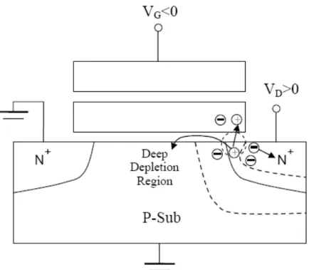
2.1.3 Band to Band Tunneling (BTBT)
In MOS structures, band-to-band tunneling typically occurs at high source or drain voltage and low gate voltage. In Flash memory devices, these conditions
- 24 -
take place in cells under erase operations, or in unselected cells sharing the same bit line with a cell under programming. BTBT contributes to the so called Gate Induced Drain Leakage current (GIDL) [44-45] , which can be a significant fraction of the subthreshold drain leakage current and can compromise proper functioning of the substrate bias generators.
Band to band tunneling application to nonvolatile memory was first proposed in 1989. I. C. Chen and et al. demonstrated a high injection efficiency (~1%) method to programming EPROM devices [46]. Band-to-band Tunneling (BTBT) process occurs in the deeply depleted doped surface region under the gate to drain or gate to source overlap region. Figure 2-5 shows the band diagram of a MOS and illustrates BTBT mechanism. In this condition, the band-to-band tunneling current density is expressed as
𝐽𝑏−𝑏 =√2𝑚 ∗𝑞3𝜀𝑉 𝑎𝑝𝑝 4𝜋3ħ2𝐸 𝑔 1 2 𝑒𝑥𝑝 ⎣ ⎢ ⎢ ⎡ −4�2𝑚∗𝐸𝑔 3 2 3𝑞𝜀ħ ⎦ ⎥ ⎥ ⎤ … … 𝑒𝑞. 2 − 5
2.1.3-(a) Band to Band Hot Electron Tunneling Injection
When band-bending is higher than the energy gap of the semiconductor, the tunneling electron from the valence band to the conduction band becomes significant. The mechanism is at the condition for positive gate voltage and negative drain voltage. Hence, the hot electrons are injected through the tunnel oxide and then recombine the stored holes as shown in Figure 2-6.
- 25 -
The injection is applied for p-type substrate nonvolatile memory device. The mechanism is at the condition for negative gate voltage and positive drain voltage. Hence, the hot holes are injected through the tunnel oxide and then recombine the stored electrons as shown in Figure 2-7.
2.2 Nonvolatile Memory Device Reliability
For a nonvolatile memory, the performance worthy to concern is distinguishing between two states of memory cell. However, in many times operation and charges storage for a long term, the states are not easily distinguishable because of charges loss. The nonvolatility of NVM implies at least 10 years of charge retention, and the cell has to store information also after many read/program/erase cycles. Endurance (also called Cycling) and retention experiments are performed to investigate Flash memory cell reliability.
2.2.1 Retention
In any nonvolatile memory technology, it is essential to maintain data for over ten years. This means the loss of charge stored in the storage medium must be as minimal as possible. For instance, in 16Mbit Flash cell, floating gate capacitance is approximately 1fF, a threshold voltage shift of 3V is requested, and a programmed cell stores around 10,000 electrons in its floating gate. A loss of only 10% in this number can lead to a wrong read of the cell; therefore a loss of less than 2 electrons per week can be tolerated.
For SONOS memory devices, data are represented as electrons stored in the silicon nitride layer, the stored electrons leak away from the trapping layer
- 26 -
through the tunnel oxide or through the interpoly dielectrics; moreover, the lateral migration of charges trapped in the silicon nitride layer also result in the wrong information [47-48]. Possible causes of charge loss are: (1) by tunneling or thermionic emission mechanisms; (2) defects in the tunnel oxide; and (3) de-trapping of charge from insulating layers surrounding the storage medium.
First, several discharge mechanisms may be responsible for time and temperature dependent retention behavior of nonvolatile memory devices. Figure 2-8 shows a band gap diagram of a SONOS device in the excess electron state, illustrating trap-to-band tunneling, trap-to-trap tunneling, and band-to-trap tunneling, thermal excitation and Poole-Frenkel emission retention loss mechanisms [49]. These mechanisms may be classified into two categories. The first category contains tunneling processes which are not temperature sensitive (trap-to-band tunneling, trap-to-trap tunneling and band-to-trap tunneling). The second category contains the other mechanisms which are temperature dependent. Moreover, trapped electrons may redistribute vertically inside the nitride by Poole–Frenkel emission, which will give rise to a shift in the threshold voltage.
Secondly, the generation of defects in the tunnel oxide can be divided into an extrinsic and an intrinsic one. The former is due to defects in the device structure; the latter to the physical mechanisms which are used to program and erase the cell. Finally, electrons can be trapped in the insulating layers surrounding the storage medium during wafer processing. The electrons can subsequently de-trap with time, especially at high temperature. However, the charge variation results in a variation of the storage medium potential.
- 27 -
Retention capability of Flash memories has to be checked by using accelerated tests which usually adopt high electric fields and hostile environments at high temperature.
2.2.2 Endurance
Endurance is the number of erase/write operations that the memory can still complete and continue to operate as specified in the data sheet. In general, Flash cells are requested to guarantee 105 program/erase cycles. This endurance requirement is sufficient for the user to take 700 photos with a 1MB size every day for 10 years [48]. As the experiment was performed applying constant pulses, the variations of program and erase threshold voltage levels are described as “program/erase threshold voltage window closure” and give a measure of the tunnel oxide aging [50-51]. In particular, the reduction of the programmed threshold with cycling is due to traps generation in the oxide and interface state generation at the drain side of the channel. The evolution of the erase threshold voltage reflects the dynamics of net fixed charge in the tunnel oxide as a function of the injected charge. The initial lowering of the erase is due to a pile-up of positive charge which enhances tunneling efficiency, while the long-term increase of the erase is due to a generation of negative traps.
The endurance characteristics give the memory threshold voltage window, which is the threshold voltages difference between the programmed state and the erased state. It is the parameters to describe how reliable is a nonvolatile memory cell. The program/erase cycles are usually measured by the FN tunneling or channel hot electron injection mechanism under room temperature
- 28 -
environment.
2.3 High-k Material as Trapping Layer
In order to improve the programming speed and/or lower the programming voltage of a SONOS-type memory device, it is desirable to use a trapping material with a lower conduction band edge (higher electron affinity) to achieve a larger offset φo, as well as to provide for programming by direct tunneling at low voltages. Recently, high-k (“high-permittivity”) dielectric materials such as HfO2 and ZrO2 have been investigated to replace thermal oxide as the MOSFET
gate dielectric [52-53]. A comparison of dielectric material properties is given in Table 2.1. Such materials have a lower conduction band edge than does silicon nitride. Thus, it should be advantageous to use a high-k material as the trapping layer in a SONOS-type memory device, provided that it contains a sufficient density of deep trap states. The electron trap level Et has been reported to be 1.0 eV for ZrO2 [52]; it has been reported to be 1.5eV for JVD HfO2 [53]. In
principle, the trap density and trap energy level in a high-k trapping layer can be tuned by adjusting the deposition process parameters.
For SOHOS (Poly-Silicon/Oxide/High-k/Oxide/Silicon) devices, the charges may be trapped in electron and hole traps in the HfO2 layer or by charge
confinement in the quantum well. From the ideal energy band diagrams of SONOS and SOHOS structures shown in Fig. 2-9 (a) and (b), respectively, the quantum well formed by the conduction band is deeper for the SOHOS structure as compared to the SONOS structure (1.6 eV compared to 1.05 eV) [54-55]. Therefore, at the same gate bias where modified Fowler–Nordheim (MFN)
- 29 -
tunneling dominates, the electrons must tunnel through a thicker energy barrier in SONOS to the conduction band of the charge storage layer (Si3N4) as
compared to SOHOS. The conduction band offset of Si3N4 with respect to
silicon is 2.05 eV, as compared to a 1.5 eV conduction band offset of HfO2 with
respect to silicon. This is illustrated in Fig. 2-10, where the modified F–N tunneling consists of direct tunneling through the thin tunnel oxide layer and F–N tunneling through the charge storage layer. Hence, electron tunneling and storage in the quantum well will be easier in SOHOS as compared to SONOS devices.
- 30 -
- 31 -
Fig 2-1: The procedure of channel hot electrons injection (CHEI).
Fig 2-2: The approach of FN programming method, when |𝐸𝑜𝑥| > 𝑋𝛷1
- 32 -
Fig 2-3: The approach of MFN programming method, when 𝛷1−𝛷2
𝑋𝑂𝑇 > |𝐸𝑂𝑇| >
𝛷1−𝛷2
𝑋𝑂𝑇+ (𝜀𝜀𝑂𝑋𝑁 )𝑋𝑁
Fig 2-4: The approach of TAT programming method, when 𝛷3 𝑋𝑂𝑇 > |𝐸𝑂𝑇| > 𝛷3 𝑋𝑂𝑇 + (𝜀𝜀𝑂𝑋 𝑁 )𝑋𝑁 , 𝛷3 = 𝛷1 − 𝛷2−𝛷𝑡
- 33 -
Fig 2-5: Band diagram of a MOS structure along the vertical direction through the depletion region illustrating band-to-band and trap-to-band tunneling mechanisms.
V
G>0- 34 -
Fig 2-7: The procedure of band to band hot holes injection.
Fig 2-8: Bandgap diagram of a SONOS device in the excess electron state, showing retention loss mechanisms: trap-to band tunneling (T-B), trap-to-trap tunneling (T-T), band-to-trap tunneling (B-T), thermal excitation (TE) and Pool-Frenkel emission (PF).
- 35 -
Fig 2-9: Ideal energy band diagrams for (a) SONOS and (b) SOHOS structures.
Fig 2-10: Energy band diagram schematic of the SONOS structure with HfO2
(solid lines) or Si3N4 (dashed lines) as the charge storage layer during write
- 36 -
CHAPTER 3
Device Fabrication and Characterization
3.1 Introduction
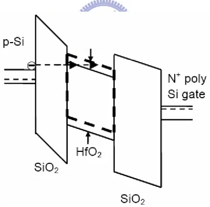
Poly silicon–oxide–nitride–oxide–silicon (SONOS) Flash memory is one of the most attractive candidates to realize Flash memory vertical scaling. Reducing the tunnel oxide thickness has been previously accomplished in order to increase the program speed and decrease the operation voltage of SONOS devices. However, this degrades the charge-retention capability of the device seriously. To overcome those limitations, the poly silicon–oxide–high-k–oxide–silicon (SOHOS) Flash memory has been attempted by replacing the silicon nitride layer with a high-dielectric constant (high-k) material.
The high-k memory structure has attracted much attention for nonvolatile Flash memory device due to its superior charge trapping properties compared to the conventional poly silicon floating gate. The SOHOS structure stores charges in spatial deep level traps, making it less vulnerable to a single defect in the tunnel oxide. This significantly helps to minimize the discharge of the memory cell [56]. During the program operation of the SOHOS n-channel transistor device, electrons tunnel through the tunnel oxide and are stored in the deep level traps [57]. During the erase operation under negative gate bias, electrons, trapped in the high-k material, are de-trapped and tunnel through the oxide layer from the charge storage layer into the silicon substrate. The SOHOS structure, using hafnium oxide (HfO2) as the charge storage layer, demonstrates a superior
- 37 -
less over-erase problems compared to conventional SONOS devices. Therefore, the HfO2 material is selected in our research [78].
While there are many advantages of using HfO2 as trapping layer, the
retention performance of HfO2 is worse than Si3N4 actually. In order to improve
the retention performance, we use CF4 plasma treatment to diffuse fluorine into
HfO2 after HfO2 is deposited. The fluorine is incorporated into the HfO2 trapping
layer and then formed of Hf-F bonding with hafnium. Because of CF4 plasma
treatment, the shallow traps would be recovered by the fluorine but the deep traps would still be left. The carriers’ de-trapping effect is decreased after program operation. Hence, the retention performance would be better.
We probe into the electrical characteristics of the capacitors and the HfO2
SOHOS memory devices. From fundamental electric characteristic data, we could know retention information. In materials analysis, we also use XPS and to analyze the devices which were carried out CF4 plasma treatment to confirm if
there is the Hf-F bonding. Besides, SIMS analyses show depth profiles of fluorine in the devices.
3.2 Experimental Procedures
In this study, we make the HfO2 capacitors and the SOHOS memory device of
different recipes. The detail of all process parameters (also called split table) will be describes later.
3.2.1 Fabrication of HfO
2Capacitor
- 38 -
of the proposed HfO2 capacitors. The fabrication processes of the capacitors
were carried out on 6-inch p-type (100)-oriented silicon substrate wafers. The resistivity of the wafer is about 15-25 Ω cm. First of all, the wafers were cleaned down by standard RCA cleaning. Before the tunnel oxide film was deposited, the all wafers were dipped into diluted HF solution to remove the chemical oxide which grown during the standard RCA cleaning.
Subsequently, the cleaned wafers were grown about 30 Å dry oxide as tunnel oxide layer through Atmospheric Pressure Chemical Vapor Deposition (APCVD) at 900℃. Then, 50 Å HfO2 film was deposited by Metal organic Chemical
Vapor Deposition (MOCVD). After 50 Å HfO2 film was deposited, the wafers
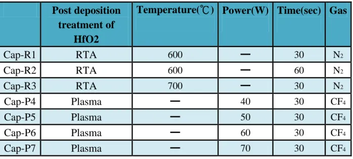
were carried out the different post deposition treatments including Rapid Temperature Annealing (RTA) and CF4 plasma treatment. The split table of post
deposition treatments is listed in Table 3.1. Afterward, about 150 Å SiO2,
composed of tetraethoxy silane (TEOS), was deposited by Plasma Enhanced Chemical Vapor Deposition (PECVD) as blocking oxide.
To form the top electrode, about 5000 Å aluminum (Al) metal film was deposited by Dual E-gun evaporate deposition system. Then, the Al film was patterned to define the capacitors. Before the lower electrode film deposition, the backside native oxide must be stripped by using Buffered Oxide Etchant (BOE) to reduce the contact resistance. Finally, a 5000 Å Al film was also deposited on the backside of the wafers as the lower electrode of the capacitors.
In the same process condition, a fluorine distribution profile across the 50Å trapping layer was revealed by SIMS (secondary ion mass spectrometry) in Fig 3-3. Apparent high fluorine concentration with a peak located at the HfO2 top
- 39 -
surface is observed. Such high fluorine concentration is more helpful in recovering traps in HfO2. Moreover, the lower fluorine concentration at the
interface lying in between tunnel oxide and Silicon substrate also slight improves the reliability of the devices.
3.2.2 Fabrication of HfO
2Trapping Layer Memory Device
Figure 3-2 (a)-(b) schematically depicts the cross section and the process flow of the SOHOS Flash memory cell using HfO2 as trapping layer. The
experimental processes of the memory device were carried out on 6-inch p-type (100)-oriented silicon substrate wafers. The resistivity of the wafer is about 15-25 Ω cm. First of all, the wafers were cleaned down by standard RCA cleaning. Before the tunnel oxide film was deposited, the all wafers were dipped into diluted HF solution to remove the chemical oxide which grown during the standard RCA cleaning. Subsequently, the cleaned wafers were grown about 30 Å dry oxide as tunnel oxide layer through APCVD at 900℃. Then, 50 Å HfO2
film was deposited by MOCVD.
In the same way, the characteristics of HfO2 memory devices should be
compared between the control and experimental samples. After 50 Å HfO2 film
was deposited, the wafers were carried out the CF4 plasma treatment
(experimental samples) or not (control samples). The split table of post deposition treatments is listed in Table 3.2. Afterward, about 100 Å blocking oxide, composed of tetraethoxy silane (TEOS), was deposited by Low Pressure Chemical Vapor Deposition (LPCVD). The poly silicon gate 2000 Å is formed by LPCVD at 900℃ for 30 min. After poly silicon/blocking oxide/HfO2/tunnel
- 40 -
oxide stack formation, gate pattern were defined by lithography and etched back. Subsequently, the transistors underwent source/drain implantation and then the source/drain were activated by RTA at 950 ℃ for 30 s. Next, the SiO2,
composed of TEOS, passivation layer 5000 Å was deposited by PECVD. And, the passivation layer was removed on the gate, source and drain region. We define the contact hole by lithography and etching back.
Lastly, the electrode about 9000 Å aluminum (Al-Si-Cu) metal film was deposited by Physical Vapor Deposition (PVD). The Al film was patterned and sintered to define the metal pad.
3.3 Results and Discussions
We probe into the electrical characteristics of the capacitors and the SOHOS memory devices in this section. The electrical characteristics of capacitors and SOHOS memory device are measured by HP4284 Precision LCR Meter and HP4156C Precision Semiconductor Parameter Analyzer.
3.3.1 Electrical Characteristic of HfO
2Capacitor
Fig 3-4(a) is the C-V hysteresis curve of capacitors with RTA and CF4 plasma
treatment after bidirectional sweeps. Because electrons inject into trapping layer from substrate the counterclockwise direction of the hysteresis curve is present. At first the upper electrode of capacitor was biased from positive voltage to negative voltage, and the inversion layer of silicon substrate turned into the accumulation layer gradually. When the capacitor was operated in the positive gate voltage, the electrons of inversion layer inject into the trapping layer
- 41 -
through F-N tunneling mode. Then these electrons will be trapped in the HfO2
layer and let the VFB (flat-band voltage) of capacitor shift to the positive side.
On the other hand, when the capacitor is biased from negative voltage to positive voltage, the trapped electrons maybe tunnel back to substrate or the holes can also inject into the trapping layer and combine with the trapped electrons. These two phenomena can reduce the amount of trapped electrons in charge storage layer and form the left C-V curve. The memory window characteristics of capacitors with RTA and CF4 plasma treatments form
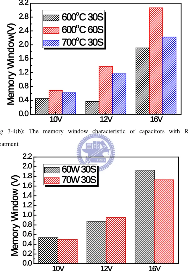
capacitance-voltage (C-V) hysteresis are respectively shown in Fig 3-4(b) and (c). In general, the larger operation voltage should cause larger memory window. The different treatments are confirmed to this rule in our experiment. From Fig 3-4(b), the memory window is depended on the temperature and duration of the RTA treatments. Because the higher temperature and the longer duration RTA make HfO2 more crystallized, the more traps are induced. Therefore, the carriers
are easily trapped in HfO2 trapping layer and then they result the larger memory
window. The memory window of Cap-P6 and Cap-P7, shown in Fig 3-4(c), are almost the same as they make HfO2 similarly crystallized. In addition, the
memory window characteristics of capacitors with the RTA and CF4 plasma
treatment also are compared in Fig 3-4(d). The memory window of Cap-P6 and Cap-P7 are like Cap-R1 and lower than Cap-R2 and Cap-R3 for the level of HfO2 crystallized. According to the x-ray diffraction (XRD) spectra of
crystallized HfO2 with RTA and CF4 plasma treatment, shown in Fig 3-5, we can
certify the level of HfO2 crystallized. It shows HfO2 with Cap-P5 is slightly
- 42 -
characteristics of different treatments by gate voltage sweeping from 0 V to 12 V and 0 V to -12 V are shown in Fig 3-6. It is clear that the gate leakage current of the capacitors containing RTA and CF4 plasma treatment are low regardless
of forward bias or reverse bias. Even thought Cap-R3 is higher than others because of seriously HfO2 crystallized, it is still lower than 10-9A. This result
can verify that CF4 plasma treatment would not induce more gate leakage current
than RTA treatment and there is no critically gate injection problem which will affect the memory window of capacitors.
Next, we begin to concern about the reliability of capacitors. Fig 3-7(a),(b) show the retention characteristic of capacitors with RTA and CF4 plasma
treatment at room temperature. From Fig 3-7(a), there is the larger VFB shift window between program state and initial state in Cap-R1 than Cap-R2 and Cap-R3 after 104 second. The capacitors, underwent lower temperature and shorter duration RTA treatments, performs the better retention characteristic. The data retention degradation attributes to the charge loss. Some possible causes of charge loss are defects in tunnel oxide, defects in blocking oxide or mobile ion contamination. Therefore, we thought that higher temperature and longer duration will induce more traps with shallower energy level in the trapping layer, which give rise to larger memory window and poor charge retention [64]. Besides, the higher temperature and longer duration make HfO2
more crystallized and there are the leakage paths formed by grain boundary. From Fig 3-7(b), we discuss capacitors with CF4 plasma treatment ,including
Cap-P4、Cap-P5、Cap-P6 and Cap-P7, and find that the retention performance is improved with increasing the power of CF4 plasma treatment. In other words,
- 43 -
Cap-P7 owns the best retention performance in all capacitors. We consider the power of Cap-P7 has enough energy to make the fluorine incorporated into the HfO2 trapping layer and then formed of Hf-F bonding with hafnium [79]. Hence,
the shallow traps would be recovered by the fluorine but the deep traps would still be left. The carriers’ de-trapping effect is decreased after program operation. The Fig 3-7(c) is the Comparisons of the retention characteristics for RTA and CF4 plasma treatment capacitors. The retention performance of Cap-P7 is better
than Cap-R1 for the shallow traps recovered by the fluorine even though they make HfO2 similarly crystallized. In order to confirm that Hf-F bonding is
formed, we analyze the XPS spectra for Hf 4f core levels from HfO2. The peak
of binding energy with 600℃ 30sec RTA treatment, shown in Fig 3-8(a), at 16.26 eV is evident and with 70W 30sec CF4 plasma treatment is at 16.64eV as
we can see in Fig 3-8(c). The bonding energy of Cap-P7 is higher than Cap-R1. This phenomenon means that there is another Hf bonding formation in Cap-P7. Hence, we consider the HfO2 with the CF4 plasma treatment reveals the Hf–F
bonding, indicating fluorine incorporation after carried out the CF4 plasma
treatment.
However, we should discuss whether the CF4 plasma treatment causes damage
on HfO2 surface in our experiment or not. The comparisons of the surface
roughness for HfO2 with RTA and CF4 plasma treatment by AFM are shown in
Fig 3-9. The surface roughnesses of them are all similar. In addition, if the CF4
plasma treatment causes damage on HfO2 surface, it will decrease thickness of
HfO2. The Fig 3-10 shows the difference of the thicknesses for HfO2 between