Recessed Oxynitride Dots on Self-Assembled Ge Quantum Dots
Grown by LPD
P.-S. Kuo,aB.-C. Hsu,aP.-W. Chen,aP. S. Chen,band C. W. Liua,b,z
aDepartment of Electrical Engineering and Graduate Institute of Electronics Engineering, National Taiwan University, Taipei, Taiwan
bElectronics Research and Service Organization of the Industrial Technology Institute, Hsinchu, Taiwan
Recessed oxynitride dots deposited on self-assembled Ge dots are demonstrated using liquid-phase deposition共LPD兲. By adding ammonia into the solution, the nitrogen atoms can be incorporated into the deposited film. The tensile strain of the Si cap layer directly deposited on Ge dots can enhance the oxynitride nucleation and deposition on Si surface. The tensile strain may also increase the etching rate of the Si cap layer and the recessed dots are formed directly above the Ge dots. The LPD-SiON dots have a higher dot step height as compared to LPD-SiO2dots.
© 2004 The Electrochemical Society. 关DOI: 10.1149/1.1785911兴 All rights reserved.
Manuscript submitted October 9, 2003; revised manuscript received February 28, 2004. Available electronically August 30, 2004.
Si/SiGe electro-optical devices are of great interest in optoelec-tronics and high-speed elecoptoelec-tronics due to their ability for integration with Si technology. The metal-oxide-semiconductor共MOS兲 tunnel-ing photodetectors with Ge/Si quantum dot absorption layers are demonstrated with low dark current and high efficiency.1,2To avoid Ge/Si material degradation such as strain relaxation and Ge out-diffusion during high-temperature processing, a low-temperature liquid-phase deposition共LPD兲 process has been used to form gate dielectrics.3 The strain-induced oxide dots are formed due to the tensile strain on the Si cap layer above the Ge quantum dots.4In this article, oxynitride films are deposited on self-assembled Ge/Si quan-tum dots and the characteristics of the oxynitride dots are investi-gated with atomic force microscopy 共AFM兲, secondary-ion mass spectroscopy共SIMS兲, and transmission electron microscopy 共TEM兲. Ge/Si quantum dots were prepared by ultrahigh-vacuum chemi-cal vapor deposition共UHVCVD兲 on p-type Si共001兲 substrate. After a Si buffer layer of 50 nm, 20 periods of Ge/Si bilayers were grown to form the self-assembled Ge dots at 600°C under Stranski-Krastanov共SK兲 growth mode.5The Si spacer layer between Ge dots was 20 nm thick. A 3 nm共nominal thickness兲 Si cap was deposited as a top layer on Ge dots for the subsequent LPD process. All layers grown by UHVCVD were unintentionally doped with an estimated hole concentration of⬃1 ⫻ 1016cm⫺3.
LPD was used for SiO2 formation with the advantages of low
thermal budget, low cost, and high throughput. A simplified mecha-nism of LPD growth was proposed originally by Nagayama et al.6 based on the reaction of H2SiF6with water to form hydrofluoric acid
and solid SiO2
H2SiF6⫹ 2H2O SiO2⫹ 6HF 关1兴
In this article, the LPD method with H2O addition only is used and
the detailed experimental flow diagram of this LPD process can be found in Ref. 3 and 7. The LPD oxynitride film was deposited by adding NH4OH into the solution saturated with silica, which is
dif-ferent from the method proposed in Ref. 8, where additional H3BO3
chemicals were added.
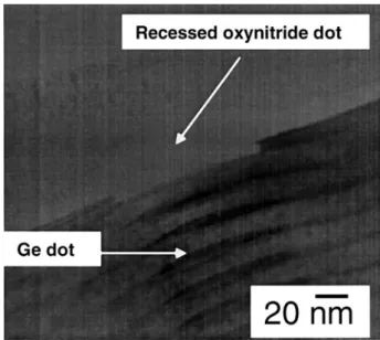
Figure 1 shows the cross-sectional TEM image of the 20-period Ge dot structure. The base width and the height of each Ge dot are about 100 nm and 6 nm, respectively. Because the spacer is smaller than the correlation length, the Ge dots are self-assembled in a row vertically in the same position.9Above the Ge dots, the recessed LPD-SiON dots are formed by adding 0.5 M NH4OH during the
LPD process. The typical SiON dot has a height of 22 nm and a wetting layer of 10 nm after 20 min growth. Note the definition of dot height is the vertical distance between the top of the dot and the wetting layer. Due to the relaxation of Ge dots, the Si cap area
directly on the Ge dots has tensile strain, while the Si cap area above the Ge wetting layer is strain free. During the oxynitride deposition process, the ionized NH4⫹, H⫹, F⫺ions incorporate into the
depos-ited film. The ions may diffuse to the Si cap/oxynitride interface and attack the Si cap surface. Therefore, the Si cap is also etched during the deposition. The tensile strain probably enhances the etching rate of Si cap directly above the Ge dots. Therefore, the oxynitride is deposited in the recess and the recessed oxynitride dot is formed 共Fig. 1兲.
To confirm that the tensile strain can enhance the oxynitride deposition rate, both the tensile-strained Si sample and the control Si sample were studied. Figure 2 shows the oxynitride film thickness vs. deposition time for both samples and the structure of the strained Si sample is shown in the inset. The strained Si sample yielded a thicker film as compared to the control Si sample. Therefore, the enhanced deposition rate above the Ge dot probably comes from the tensile strain of the Si cap layer.
The SIMS profiles of O, N, and Ge atoms of the LPD oxynitride film with 1 M NH4OH in the solution are shown in Fig. 3. The
SIMS profile was performed by Cs ion source with 2 keV energy. The increase of Ge signal as the number of deposition layers in-creased indicates the size increase of the Ge quantum dots, as con-firmed by TEM micrograph共Fig. 1兲. However, the Ge signal of the top layer is smaller as compared to the second and third Ge layer due to the top Ge layer being etched by NH4OH. The estimated O:N
zE-mail: [email protected]
Figure 1. Cross-sectional TEM micrograph of recessed oxynitride dots on self-assembled Ge quantum dots.
Electrochemical and Solid-State Letters, 7共10兲 G201-G203 共2004兲
1099-0062/2004/7共10兲/G201/3/$7.00 © The Electrochemical Society, Inc.
G201
ratio is 16:7 at N peak position共⬃55 nm from the surface兲. Note that the N and O are piled up at⬃55 nm, and the first Ge peak is also located at⬃55 nm, indicating that both the Si cap and the top Ge layer were etched during deposition and the oxynitride/Ge inter-face is about 55 nm in depth.
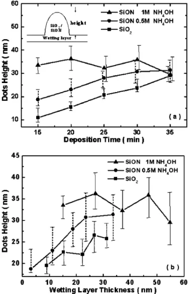
From the TEM image, the oxynitride wetting layer is 10 nm thick, similar to the LPD-SiON thickness on the control Si samples under the same growth condition. The thickness of LPD-SiON on control Si sample can be measured by ellipsometry. The step height 共22 nm兲 of the LPD-SiON dots also agrees well with the AFM results. Therefore, the AFM morphology and the film thickness mea-sured by ellipsometry on control Si samples were used to character-ize the SiON dots height and the wetting layer thickness, respec-tively. Figure 4a shows the average dot height of LPD-SiO2 and
LPD-SiON共0.5 M and 1 M NH4OH) dots vs. deposition time. The
LPD-SiON had a higher deposition rate as compared to the LPD-SiO2, and the deposition rate increased as ammonia
concen-tration increased. The dot height vs. wetting layer thickness is shown in Fig. 4b. Under the same wetting layer thickness, the LPD-SiON dots still yielded a higher dot height. The LPD-SiON dots with 1 M NH4OH concentration were the tallest, and the dot height almost did
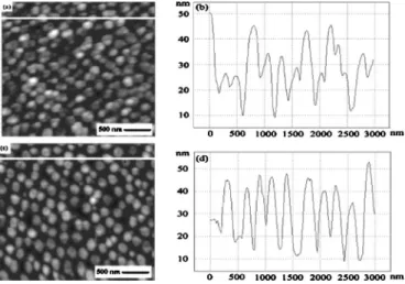
not change with deposition time. The AFM images of oxide and oxynitride dots with similar wetting layer thicknesses are shown in Fig. 5a and c, respectively, and the corresponding cross-sectional morphologies are illustrated in Fig. 5b and d. Because the deposition rate for oxynitride is much higher than that for oxide, the deposition time for oxide was longer to have the same wetting layer thickness. From Fig. 5b and d, the oxynitride dots are more uniform in lateral size and height as compared to oxide dots. The dot densities of oxide and oxynitride dots are 2.1⫻ 109 and 1.7⫻ 109 cm⫺2,
respec-tively. The higher dot density of oxide dots is owing to the over-lapped small dots, as shown in Fig. 5b. The oxide and oxynitride dots have an average base width of 188 and 173 nm, respectively 共not including the overlapped small dots兲.
To have a metal-insulator-semiconductor共MIS兲 structure, alumi-num was deposited on 1.5 nm LPD oxide and oxynitride films and was patterned to form MIS diodes10 with a circular area of 3 ⫻ 10⫺4cm2. For MIS tunneling devices with insulators less than 3
nm thick, the minority carrier generation rate in the deep depletion region dominates the dark current at inversion bias.11 The LPD-SiON device had a lower inversion current as compared to LPD-SiO2device due to the N atoms at the interface to passivate the
Figure 2. Oxynitride film thickness vs. deposition time for both
tensile-strained Si and control Si samples. The inset shows the structure of the strained Si sample.
Figure 3. SIMS profiles of O, N, and Ge atoms of LPD oxynitride on 20
layer Ge quantum dots. The increase of the Ge signal as the number of deposition layers increases indicates the size increase of the Ge quantum dots, as confirmed by TEM micrograph.
Figure 4. 共a兲 Dot height of LPD oxide and oxynitride vs. deposition time.
The measured thickness on the control Si wafers is similar to the wetting layer thickness.共b兲 Dot height vs. wetting layer thickness. The oxynitride dots are taller than oxide dots with the same wetting layer thickness. Note that the solid symbols are the average value of measurement data. The upper and lower error bars are the maximum and minimum of the measured data. Electrochemical and Solid-State Letters, 7共10兲 G201-G203 共2004兲
G202
interface states and to have a smaller interface state density (Dit)3.
In conclusion, the tensile strain on the Si cap above self-assembled quantum dots probably can enhance the etching rate of Si and have a preferential oxynitride deposition on Ge dots during
LPD. The recessed oxynitride dots are demonstrated with larger dot height as compared to oxide dots. Due to N atom passivation of the interface states, the device with oxynitride yields a lower dark cur-rent as compared to an oxide device.
Acknowledgment
This work is supported by National Science Council, Taiwan, R.O.C., under contract no. NSC 2120-E-002-006 and NSC 92-2215-E-002-007. TEM assistance by S. W. Lee, National Tsing Hua University, is also highly appreciated.
National Taiwan University assisted in meeting the publication costs of this article.
References
1. B.-C. Hsu, S. T. Chang, T.-C. Chen, P.-S. Kuo, P. S. Chen, and C. W. Liu, IEEE
Electron Device Lett., 24, 318共2003兲.
2. B.-C. Hsu, S. T. Chang, C.-R. Shie, C.-C. Lai, P. S. Chen, and C. W. Liu, Tech. Dig.
- Int. Electron Devices Meet., 2002, 91.
3. B.-C. Hsu, W.-C. Hua, C.-R. Shie, K.-F. Chen, and C. W. Liu, Electrochem.
Solid-State Lett., 6, F9共2003兲.
4. C. W. Liu, B.-C. Hsu, K.-F. Chen, M. H. Lee, C.-R. Shie, and P.-S. Chen, Appl.
Phys. Lett., 82, 589共2003兲.
5. D. J. Eaglesham and M. Cerullo, Phys. Rev. Lett., 64, 1943共1990兲.
6. H. Nagayama, H. Honda, and H. Kawahara, J. Electrochem. Soc., 135, 2013
共1988兲.
7. J.-S. Chou and S.-C. Lee, Appl. Phys. Lett., 64, 1971共1994兲.
8. M. K. Lee, S. Y. Lin, and J.-M. Shyr, J. Electrochem. Soc., 148, F1共2001兲. 9. O. G. Schmidt and K. Eberl, Phys. Rev. B, 61, 13721共2000兲.
10. C. W. Liu, W. T. Liu, M. H. Lee, W. S. Kuo, and B. C. Hsu, IEEE Electron Device
Lett., 21, 307共2000兲.
11. C.-H. Lin, B.-C. Hsu, M. H. Lee, and C. W. Liu, IEEE Trans. Electron Devices, 48, 2125共2001兲.
Figure 5. 共a兲 AFM surface image of LPD oxide with 15 nm wetting layer thickness after 60 min growth.共b兲 Cross-sectional morphology of LPD oxide along the line in 共a兲. 共c兲 AFM surface image of LPD oxynitride 共1 M NH4OH) with 15 nm wetting layer thickness after 15 min growth.共d兲 Cross-sectional morphology of LPD oxynitride along the line in共c兲.
Electrochemical and Solid-State Letters, 7共10兲 G201-G203 共2004兲 G203