國 立 交 通 大 學
電子工程學系 電子研究所碩士班
碩 士 論 文
鎳/氧化鉿/氮化鈦結構的電阻式記憶體
及其熱處理效應
Effect of Thermal Treatment on Resistive Random Access
Memory (RRAM) of Ni / HfO
x/ TiN Structure
研 究 生 : 陳 信 宇
指導教授 : 張 國 明 博士
鎳/氧化鉿/氮化鈦結構的電阻式記憶體
及其熱處理效應
Effect of Thermal Treatment on Resistive Random Access Memory
(RRAM) of Ni / HfO
x/ TiN Structure
研 究 生:陳信宇 Student:Hsin-Yu Chen
指導教授:張國明 博士 Advisor:Dr. Kow-Ming Chang
國 立 交 通 大 學
電子工程學系 電子研究所碩士班
碩 士 論 文
A Thesis
Submitted to Department of Electronics Engineering and Institute of Electronics
College of Electrical and Computer Engineering
National Chiao Tung University
in Partial Fulfillment of the Requirements
for the Degree of Master
in
Electronics Engineering
August 2009
Hsinchu, Taiwan
中華民國九十八年八月
鎳/氧化鉿/氮化鈦結構的電阻式記憶體
及其熱處理效應
研究生:陳信宇
指導教授:張國明 博士
國立交通大學
電子工程學系 電子研究所碩士班
摘
摘
摘
摘 要
要
要
要
在本論文中,我們使用鎳、非化學當量的氧化鉿和氮化鈦的金屬-氧化物-金 屬結構來展示電阻式記憶體的特性。可以觀察到重覆性的電阻值轉換而且平均的 電阻比例大於 100。經過氬氣退火的氧化鉿薄膜展現出大電流操作的特性,藉由 X 光繞射分析觀測到氧化鉿薄膜已經結晶,這可能是造成大電流操作的原因。為 了降低功率消耗,我們對氧化鉿進行氧退火並且使用細絲理論來解釋量測到的數 據。量測結果顯示:比起沒有氧退火的試片而言,氧退火過的試片其電流和功率 消耗都大約小 10 倍。經過氧退火製程後,操作電壓並沒有很顯著的增加,而且 耐用度也稍微改善。除此之外,資料保留特性和非破壞性讀取也在本讑文中被測 試。我們的研究顯示:退火過的鎳/氧化鉿/氮化鈦的電阻式記憶體是很有希望被 應用在低功率消耗的非揮發性記憶體。Effect of Thermal Treatment on Resistive Random Access
Memory (RRAM) of Ni / HfO
x/ TiN Structure
Student:Hsin-Yu Chen Advisor:Dr. Kow-Ming Chang
Department of Electronics Engineering and Institute of Electronics
National Chiao Tung University, Hsinchu, Taiwan
ABSTRACT
In this thesis, we used metal-oxide-metal (MOM) structure of nickel (Ni), non-stoichiometric hafnium oxide (HfOx), and titanium nitride (TiN) to demonstrate RRAM characteristics. Voltage-induced resistance switching is repeatedly observed in the Ni/HfOx/TiN device with average resistance ratio greater than 100. The HfOx film which is annealed in Ar ambient exhibits large current operation. It is probably due to crystallization of HfOx film by X-Ray Diffraction (XRD) result. In order to reduce power dissipation, HfOx is oxygen annealed and we use filamentary model to explain the measured data. Measurement result shows that all operation current and power are smaller about 10 times than the sample which is not annealed in O2 ambient. Operation voltage is not elevated noticeably and endurance is slightly improved after oxygen annealing process. Besides, data retention and non-destructive readout are tested in this thesis. Our study shows that the annealed Ni/HfOx/TiN RRAM is a promising candidate for low power nonvolatile memory applications.
誌
誌
誌
誌
謝
謝
謝
謝
在碩士求學時間裡,首先要感謝我的指導老師張國明教授,使我在研究或做 人處世上都獲益良多。此外,感謝王水進老師、鄧一中老師和賴瓊惠老師在口試 中,對本論文內容提出的建議及看法,讓我對研究的題目有更進一步的想法。 其次感謝實驗室學長們的熱心指導,尤其是曾文賢學長,提供試片並給予訓 練和意見,黃菘宏學長給予旁觀者的看法和觀點,使我能用不同的角度去思考。 另外也感謝國家奈米元件實驗室(NDL)與國立交通大學奈米中心(NFC)提供完善 的研究環境和設備,以及張妙如小姐、何惟梅小姐、簡秀芳小姐及姚潔宜小姐等 人的熱心協助,讓我的研究和論文可以很順利的完成。 在新竹求學的日子,感謝交大電子物理系和交大電子研究所對我的栽培,李 清音小姐在我低潮時的鼓勵,實驗室同學和其他實驗室朋友的幫忙與照顧,實驗 夥伴吳天佑、賴威仁、廖彥凱、學弟黃俊傑和林煒力對實驗的付出。亦要感謝下 列獎學金的資助,使我能無後顧之憂專心求學,新竹城隍廟獎學金,黃顯雄、劉 秀蓮獎學金,林公熊徵學田基金會獎學金,宗倬章先生教育基金會獎助學金,公 益信託崇貿環保節能教育基金會獎學金。 最後,要特別感謝家人對我的支持,女友卉馨的陪伴,讓我能順利完成我的 學業,取得碩士學位。 陳信宇于新竹交大 2009 年 8 月
CONTENTS
摘要 ...i
ABSTRACT ...ii
誌謝 ...iii
CONTENTS ...iv
TABLE CAPTIONS ...vi
FIGURE CAPTIONS ...vii
CHAPTER 1 INTRODUCTION...1
1-1 Overview of Nonvolatile Memory ...1
1-2 Nano CMOS and High-κ Material ...2
1-3 Resistive Random Access Memory...3
1-4 Typical Switching Operation and Model of RRAM ...4
1-5 Filamentary Model and Anode Interface...5
CHAPTER 2 EXPERIMENTAL PROCEDURE & MEASUREMENT SETUP ...9
2-1 Motivation ...9
2-2 Experimental Procedures ...9
2-3 Measurement Setup ...12
CHAPTER 3 RESULTS & DISCUSSION ...14
3-1 Definition of switching parameter ...14
3-2 Example of Switching Parameter Extraction ...16
3-3 Comparison between Control Sample and RTA in Ar Ambient ...21
3-4 Comparison between Control Sample and RTA in O2 Ambient...26
3-4-1 Time of RTA in O2 Ambient at 400oC...26
3-4-3 Compliance Current ...36
3-4-4 Summary and Comparison...39
CHAPTER 4 CONCLUSION ...42
CHAPTER 5 FUTURE WORK ...43
REFERENCES ...44
APPENDIX A DETAIL MEASUREMENT RESULT...50
A-1 Control Sample, 0.5mA...50
A-2 Ar, 400oC, 90sec, 0.5mA ...52
A-3 Ar, 500oC, 90sec, 0.5mA ...53
A-4 O2, 400oC, 30 sec, 0.5mA...54
A-5 O2, 400oC, 60 sec, 0.5mA...55
A-6 O2, 400oC, 90 sec, 0.5mA...56
A-7 O2, 500oC, 30 sec, 0.5mA...57
A-8 O2, 400oC, 30 sec, 0.1mA...58
TABLE CAPTIONS
Table 1-1 Comparison of Non-volatile Memory [1] ...2 Table 3-1 Statistical summary of control sample and RTA at 400oC and 500oC in Ar ambient for 90 seconds under 0.5 mA compliance current ...25 Table 3-2 Statistical summary of control sample and RTA at 400oC in O2 ambient for 30, 60, and 90 seconds under 0.5 mA compliance current ...31 Table 3-3 Statistical summary of control sample and RTA in O2 ambient at 400oC for 60, 90 seconds and 500oC for 30 seconds under 0.5 mA compliance current
...35 Table 3-4 Statistical summary of control sample and RTA in O2 ambient at 400oC for 30 and 60seconds under 0.1 mA compliance current ...38 Table 3-5 Summary of measured performance and comparison with the other works ...41
FIGURE CAPTIONS
Fig. 1-1 Typical switching operation of RRAM...5
Fig. 1-2 Process of filament formation and oxygen ion movement ...7
Fig. 1-3 I-V curve of uni-polar operation ...7
Fig. 1-4 Conductive filament of on state ...8
Fig. 1-5 Multi-filament of on state ...8
Fig. 1-6 Filament rupture near anode interface and conductive filament of off state ...8
Fig. 2-1 The fabricated RRAM cell, voltage polarity and current direction of measurement ...10
Fig. 2-2 XPS compositional depth profile of Ni/HfOx/TiN structure (control sample) ... 11
Fig. 2-3 AFM image of HfOx... 11
Fig. 2-4 Conceptual diagram of uni-polar operation and definition of resistive switching...13
Fig. 3-1 Definition of set and reset power ...15
Fig. 3-2 I-V curves of control sample under different compliance currents ...16
Fig. 3-3 Fifty-two I-V switching curves of control sample under 0.5 mA compliance current ...17
Fig. 3-4 (a) Vset and Vreset from Fig. 3-3 (b) histogram of Vset and Vreset from Fig. 3-3...17
Fig. 3-5 Selected I-V curves from Fig. 3-3...18
Fig. 3-6 Maximal reset current of Fig. 3-3 ...18
Fig. 3-8 Gon, Goff, Ratio of Fig. 3-3 ...20 Fig. 3-9 Forming process I-V curves of control sample and RTA at 500oC in Ar ambient for 30, 60, and 90 seconds ...22 Fig. 3-10 X-Ray Diffraction result of control sample, RTA in Ar ambient at 500oC for 30 seconds and 3 minutes ...22 Fig. 3-11 Comparison of control sample, RTA at 400oC and 500oC in Ar ambient for 90 seconds under 0.5 mA compliance current : (a) Goff (b) Gon (c) Vset (d) Vreset (e) Maximal reset current ...25 Fig. 3-12 Comparison of control sample, RTA at 400oC in O2 ambient for 30, 60, and 90 seconds under 0.5 mA compliance current : (a) Goff (b) Gon (c) Vset (d) Vreset (e) Maximal reset current ...29 Fig. 3-13 Gon, Goff, and Ratio of the sample of RTA in O2 ambient at 400oC for 90 seconds under 0.5mA compliance current ...30 Fig. 3-14 (a) Reset process I-V curves of O2 RTA at 400oC for 60 and 90 seconds samples (b) Linear fitting of reset process log I – log V curves...31 Fig. 3-15 Comparison of control sample, RTA in O2 ambient for 60 and 90 seconds at 400oC or 30 seconds at 500oC under 0.5 mA compliance current : (a) Goff (b) Gon (c) Vset (d) Vreset (e) Maximal reset current ...34 Fig. 3-16 Set process I-V curves of RTA in O2 ambient at 500oC for 60 seconds 35 Fig. 3-17 Comparison of control sample, RTA in O2 ambient at 400oC for 30 and 60 seconds under 0.1 mA compliance current : (a) Goff and Gon (b) Vset and Vreset (c) Maximal reset current ...38 Fig. 3-18 Retention test and switching cycles of RTA in O2 ambient at 400oC for 60 seconds under 0.1mA compliance current ...40 Fig. 3-19 Average of maximal reset current versus compliance current under various process conditions...40
CHAPTER 1
INTRODUCTION
1-1 Overview of Nonvolatile Memory
During the last several years, there has been a rapid growth of nonvolatile memory (NVM) due to the demand for applications to personal computer (PC) and portable device. NVM is computer memory that can retain the stored information even when powered off. NVM of common usage includes not only mechanical type, such as hard disk (HD) and digital video disk (DVD), but also electrical type, such as read-only memory (ROM) and flash memory. The advantages of small size, anti-seismic, and low power consumption make flash memory more superior in applying mobile equipment than mechanical type. Moreover, it is believed that flash memory will have higher operation speed than mechanical type in the long run.
However, flash memory is facing the downscaling limitation problem. The main difficulty is : tunnel oxide is such thin that charges stored in the floating gate will leak into the substrate through the thinner tunnel oxide. Inter-poly dielectric thickness, isolation spacing, cell-cell parasitic coupling, and number of stored charge are also issues of downscaling [1]. Therefore, several types of nonvolatile memories like ferroelectric random access memory (FeRAM), magnetic random access memory (MRAM), phase change memory (PCM), and resistive random access memory (RRAM) are under investigation. Among these nonvolatile memories, RRAM is a good candidate for a few factors: compared to FeRAM, it has non-destructive readout;
its operation voltage is lower than flash memory; its program current is lower than PCM and MRAM [2]; its operation speed is higher than PCM; compared to MRAM, its structure (Metal-Oxide-Metal) is so simple that it can be applied in 3D integration easily. Comparison of NVMs is listed in Table 1-1 [1].
Table 1-1 Comparison of Non-volatile Memory [1]
Flash PCM FeRAM MRAM RRAM
Integration Good Good Poor Poor Good
Multi Level Cell Yes Yes No No Yes
Cell Size 4F2 6F2 20F2 30F2 4F2
Current ~ µA ~ mA ~µA ~ mA < 0.1mA
Write/Erase Voltage (V) 12 3 0.9 ~ 3.3 1.5 < 3
Write/Erase Time ~ ms ~ 100ns ~ 40ns < 10ns < 10ns
Read Voltage (V) 4 ~ 5 3 0.9 ~ 3.3 1.5 0.7
Read Time 70~90ns 60ns 45ns 20ns < 50ns
Write/Erase Cycles > 105 108 1014 > 3×10¹⁶ > 105
Retention Time > 10 years > 10 years > 10 years > 10 years > 10 years
1-2 Nano CMOS and High-κ
κ
κ Material
κ
Recently, the technology, which is often applied to very-large-scale integrated circuit (VLSI), is complementary metal-oxide-semiconductor (CMOS) process. In order to achieve specification of Moore’s law, the trend of CMOS process was
downscaling of channel length and thickness of gate oxide in the past. But the downscaling led to short channel effect and increased of leakage current through gate oxide [3]. Hence, strained silicon technique is brought up to enhance carrier mobility. Metal gate is proposed to improve depletion of poly-silicon gate and enhance capability of gate control over the channel. High-κmaterial is used to relax the requirement of gate leakage current while maintaining the same capacitance. Among many proposed oxide, hafnium oxide film has great potential as high-κgate oxide due to its high dielectric constant, large energy bandgap, and compatibility with conventional CMOS process [3-6]. Furthermore, it is reported that thermal treatment, such as oxygen annealing [7, 8], enable hafnium oxide to have better performance of leakage current.
1-3 Resistive Random Access Memory
Silicon oxide has been shown to exhibit resistive switching as early as 1967 [9], and has recently been revisited [10, 11]. In addtion, perovskite oxides and transition metal oxides (TMOs) were also found to have properties of resistive switching. But TMOs have more endurance cycles than the other one [12] and they are more easily applicable to normal semiconductor manufacturing processes than perovskite oxide, which consists of more than 3 components [13]. Nickel oxide [14], copper oxide [15], tantalum oxide [16], and hafnium oxide [17] have been revealed their excellent properties of resistive switching. For the most part, hafnium oxide is the best candidate of RRAM because hafnium oxide is a well-known oxide, has more reliability studies, and is the best choice of high κ gate dielectric in CMOS technology as mentioned above.
1-4 Typical Switching Operation and
Model of RRAM
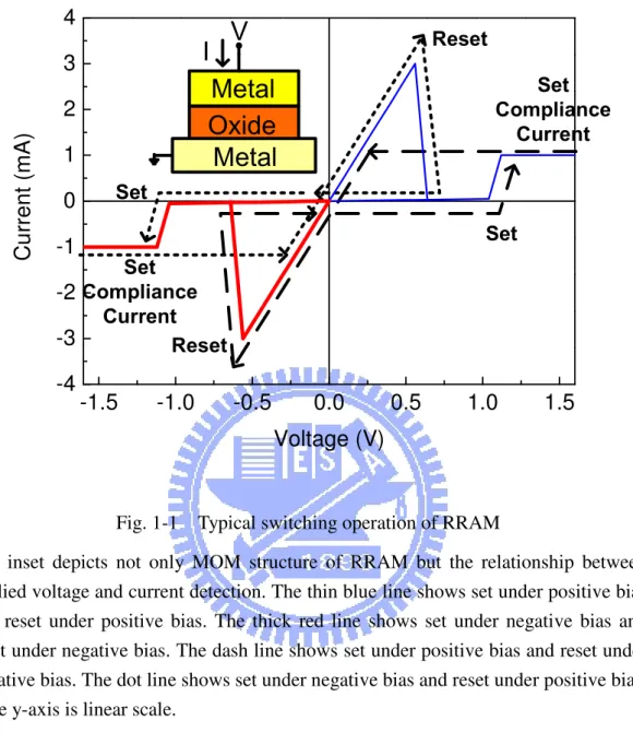
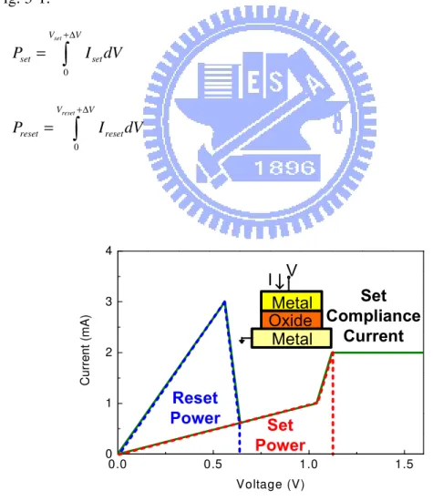
The structure of RRAM cell is metal-oxide-metal (MOM) as shown in the inset of Fig. 1-1. The relationship between applied voltage and current detection is also depicted in the inset of Fig. 1-1. Basic characterization of RRAM consists of the following methods: direct current (DC) voltage bias [18], DC current bias [19], and alternating current (AC) impedance measurement [20, 21]. Most popular is the voltage bias method that is current detection under several given bias voltage. It can set (turn on, or write) the RRAM cell from off state (i.e. low current level) to on state (i.e. high current level) and reset (turn off, or erase) from on state to off state under appropriate voltage bias. In accordance with voltage polarity, this method can be subdivided into four types schematized in Fig. 1-1. If the RRAM cell has four type operations, we call it “non-polarity” [18, 22]. If the RRAM cell only has single polarity operation, we call it “uni-polarity” [23]. If the RRAM cell belong to neither non-polarity nor uni-polarity, we call it “bi-polarity” [24]. In general, uni-polar operation is seen to be relevant to filamentary conductive path and anode interface [23]. Bi-polar operation is associated with the redox reaction and trap/detrap at the anode interface [25] or space charge limited conduction (SCLC) model [15, 17]. For commercial application, uni-polar operation is superior to bi-polar operation due to the demand for single polar supply voltage merely or no need for voltage converters. The number of write and erase is called endurance.
Set Compliance Current Set Compliance Current Set Set Reset Reset
Oxide
Metal
V
Metal
I
-1.5
-1.0
-0.5
0.0
0.5
1.0
1.5
-4
-3
-2
-1
0
1
2
3
4
C
u
rr
e
n
t
(m
A
)
Voltage (V)
Fig. 1-1 Typical switching operation of RRAM
The inset depicts not only MOM structure of RRAM but the relationship between applied voltage and current detection. The thin blue line shows set under positive bias and reset under positive bias. The thick red line shows set under negative bias and reset under negative bias. The dash line shows set under positive bias and reset under negative bias. The dot line shows set under negative bias and reset under positive bias. Note y-axis is linear scale.
1-5 Filamentary Model and Anode
Interface
Although exact resistive switching mechanism is a controversial issue, filamentary model is often used and accepted extensively. Hence, filamentary model by using DC voltage sweeping is introduced in this section. During voltage sweeping,
the voltage is applied to the top electrode and the bottom electrode is grounded. Here, uni-polar switching which is set under positive voltage and reset under positive voltage is used.
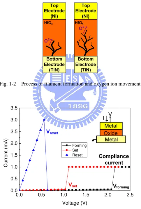
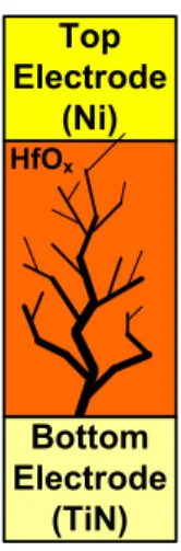
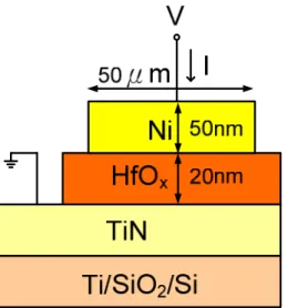
A transition metal oxide (TMO) is normally insulating without any voltage sweeping. When positive voltage is applide to top electrode, the oxygen ion (O2-) moves toward anode through oxygen vacancies as shown in Fig. 1-2 [26]. Oxygen leaving remains many oxygen vacancies which aligned together like “tree” or “filament”as depicted in Fig. 1-2 [26]. When voltage is raised to Vforming as shown in Fig. 1-3, current will suddenly increase (soft breakdown) to a certain limiting value (prevent completely breakdown [23]). That top electrode and bottom electrode are connected together by conductive filament forms on state as show in Fig. 1-4. This is called “forming process” which is initialized RRAM cell. Electron in this film can transport through these filament (or oxygen vacancy). Generally speaking, Vforming is usual positively related to oxide thickness [14, 17] and filament near anode is weaker than cathode [27]. Conductive Atomic Force Microscope (CAFM) results suggested that probably many current paths [27, 28], rather than a single filament, are involved as shown in Fig. 1-5.
Once the filament is formed, excute voltage sweep without any compliance current again. As voltage is raised to Vreset as shown in Fig. 1-3, current will reach maximal current and accumulate Joule heat. This heat results in rupture of weaker filament near anode interface [29] as showed in Fig. 1-6 and current suddenly decreases (reset) to low current level (off state). This is called “reset process” and explained why characteristic of RRAM is highly related to top electrode [30, 31]. One study indicated that the rupture thickness is about 3-10 nm [32].
The off state cell can return to on state by “set process”. Set process is similar to forming process as shown in Fig. 1-3. Vset is usually smaller than Vforming because set process only needs to construct shorter filament than forming process. Set and reset process can make the cell of state reversible.
Fig. 1-2 Process of filament formation and oxygen ion movement
0.0 0.5 1.0 1.5 2.0 2.5 0.0 0.5 1.0 1.5 2.0 2.5 3.0 3.5 C u rr e n t (m A ) Voltage (V) Forming Set Reset
HfOx Top Electrode (Ni) Bottom Electrode (TiN)
Fig. 1-4 Conductive filament of on state
Fig. 1-5 Multi-filament of on state
CHAPTER 2
EXPERIMENTAL PROCEDURE &
MEASUREMENT SETUP
2-1 Motivation
Hafnium oxide based RRAM in previous studies seldom used in uni-polar operation. One study [23] uses platinum (Pt) as top electrode, HfOx as oxide, TiN as bottom electrode to form MOM structure of RRAM. Pt hardly causes reaction with oxygen, but this inert metal is more expensive than others. We used nickel (Ni) as top electrode because of its high free energy [31] and low cost compared to inert metal.
Thermal treatment is used to improve leakage current of highκmaterial as mentioned in section 1-2. Several studies applied this technique on RRAM to enhance ratio [33] (i.e. on state current divided by off state current), decrease forming voltage [34] (i.e. first set voltage from fresh sample to on state), improve endurance [35]. Also, most of those studies focused on bi-polar operation. Hence, we used non-stoichiometric HfOx films to demonstrate effect of thermal treatment and focus on uni-polar operation, behavior of on state and off state.
2-2 Experimental Procedures
The fabrication of RRAM cell is described as follows. A TiN film as the bottom electrode was deposited on Ti/SiO2/Si by sputtering. Then, non-stoichiometric HfOx
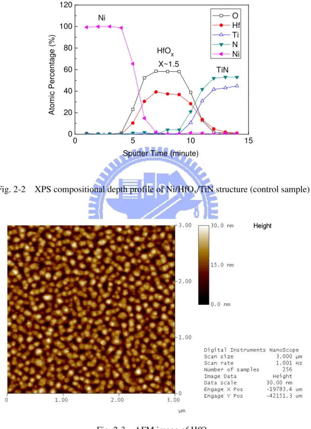
films with a thickness of 20 nm were deposited by Industrial Technology Research Institute (ITRI) using hafnium tetrachloride (HfCl4) and water (H2O) as reactants at temperature of 300OC in standard atomic layer deposition (ALD) system. After HfOx deposition, some samples were thermally annealed in a rapid thermal annealing (RTA) system at 400OC or 500OC for 30, 60, 90, and 120 seconds. Argon (Ar) and Oxygen (O2) were used as the annealing gas for the annealing systems. The samples without thermal annealing treatment are called control samples. Then, nickel (Ni) as a top electrode was deposited by E-beam evaporation using a shadow mask at room temperature. The thickness of Ni and diameter of top electrode was 50 nm and 50μm, respectively. The fabricated RRAM cell is shown in Fig. 2-1. The depth profile of the
chemical composition of HfOx films (control sample) measured by X-ray
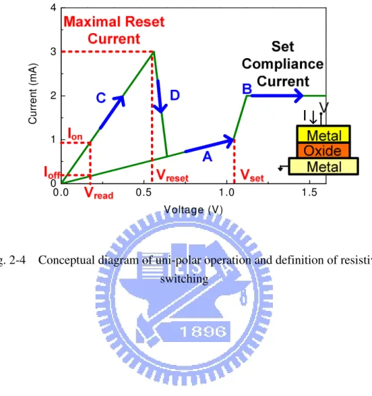
Photon–electron Spectroscopy (XPS) is shown in Fig. 2-2. The atomic ratio of oxygen to hafnium (O:Hf) inside the HfOx film is found to be about 1.5 (x < 2), which suggests that the HfOx film is non-stoichiometric. The surface morphology of HfOx samples was examined by atomic force microscopy (AFM) in tapping mode as shown in Fig. 2-3. The rms surface roughness over a scanning area of 3×3μm2 is around 4.9 nm.
Fig. 2-1 The fabricated RRAM cell, voltage polarity and current direction of measurement
0 5 10 15 0 20 40 60 80 100 120 Ni A to m ic P e rc e n ta g e ( % )
Sputter Time (minute)
O Hf Ti N Ni HfOx X~1.5 TiN
Fig. 2-2 XPS compositional depth profile of Ni/HfOx/TiN structure (control sample)
2-3 Measurement Setup
The electrical properties of the RRAM devices were measured using a Agilent 4156C semiconductor parameter analyzer. During measurement, the voltage was applied to the Ni electrode and the TiN electrode was grounded. In this thesis, we adopted DC voltage bias method. Our voltage step was 0.08 V as voltage sweeping and compliance currents were 0.1, 0.5, and 1mA. In order to achieve the purpose of low power consumption, the lower compliance current was preferable. But not all samples of different process conditions had operation of low compliance current or sufficient endurance under small compliance current.
The uni-polar operation of RRAM is described as follows and shown in Fig. 2-4. Suppose that RRAM cell is at off state. Firstly, execute voltage sweeping (A→B) and detect current. As voltage is raised to Vset, current will suddenly increase (soft breakdown, or set) to a certain limiting value (0.1~10mA). Secondly, execute voltage sweeping (C→D) and detect current without any compliance current. In general, the second current is usually larger than the first at small voltage bias and maximal reset current is usually larger than compliance current. As voltage is raised to Vreset, current will suddenly decrease (reset) to low current level (off state) and stop sweeping immediately. These step (A→B and C→D) are called one cycle. Vreset is always smaller than Vset. This is how resistance switching is observed. If the suddenly increased current is too high (>30mA), this cell is hard breakdown (never return to off state or burn out) and becomes useless. If the compliance current is too small, this cell is not switched state or small on/off ratio. Therefore, setting a proper current limit (compliance current) is crucial.
0.0 0.5 1.0 1.5 0 1 2 3 4 C u rr e n t (m A ) Voltage (V)
Fig. 2-4 Conceptual diagram of uni-polar operation and definition of resistive switching
CHAPTER 3
RESULTS & DISCUSSION
3-1 Definition of switching parameter
The switching parameter is defined in this section. As show in Fig. 2-4, the currents of on state and off state at small voltage Vread are defined as Ion and Ioff, respectively. When Vread is limited to far less than Vreset, on state and off state are not disturbed. Then, conductance of these two states at Vread are defined in Eq. (3-1) and Eq. (3-2), respectively. 1 / on on on read G =R − ≡I V (3-1) 1 /
off off off read
G =R − ≡I V (3-2)
Conductance ratio of two states is defined as Eq. (3-3). /
on off
Ratio≡G G (3-3)
Assume two states are equally probable, and then expectation value of readout
power Pread can be expressed as Eq. (3-4).
2 2
1 1 1 1
2 2 2 2
read read on read off read on read off
P = V I + V I = V G + V G (3-4)
Assume Gon>>Goff, then the term of off state can be neglected. Eq. (3-4) can be
simplified as Eq. (3-5).
2
1 1
2 2
read read on read on
To make Gon overly large gain large Ratio (= Gon/Goff) causes high readout power
as indicated in Eq. (3-5). For commercial NVM, the number of times of readout is
1012. Therefore, small readout power is significant. In order to achieve the purpose of
small readout power, Gon must be decreased as indicated in Eq. (3-5). Nevertheless,
small Gon leads to small conductance ratio as indicated in Eq. (3-3). Hence, Goff must
also be reduced for large enough ratio. Gon is only need to be large enough to
distinguish Gon from Goff.
Besides, set power [36] and reset power (power of write and erase) are defined in Eq. (3-6) and Eq. (3-7), respectively. The set power and reset power are also sketched as Fig. 3-1. 0 set V V set set P I dV +∆ =
∫
(3-6) 0 reset V V reset reset P I dV +∆ =∫
(3-7) Set Compliance Current Set Power 0.0 0.5 1.0 1.5 0 1 2 3 4 C u rr e n t (m A ) Voltage (V) Reset Power Oxide Metal V Metal I3-2 Example of Switching Parameter
Extraction
In this section, extraction and presentation of measurement result are stated
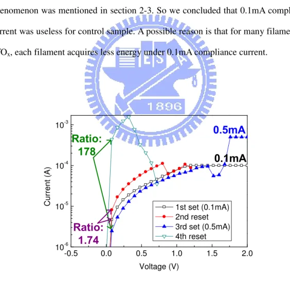
clearly by using the measurement result of control sample. From 1st and 2nd I-V curve
of Fig. 3-2, the cell in off state was not switching (only 1.74 ratio) under too small compliance current (0.1mA). In this case, we must boost compliance current to 0.5mA
to have large on/off ratio (178) as shown in 3rd and 4th I-V curve of Fig. 3-2. This
phenomenon was mentioned in section 2-3. So we concluded that 0.1mA compliance current was useless for control sample. A possible reason is that for many filaments in
HfOx, each filament acquires less energy under 0.1mA compliance current.
Ratio:
178
-0.5 0.0 0.5 1.0 1.5 2.0 10-6 10-5 10-4 10-3 Cu rr e n t (A ) Voltage (V) 1st set (0.1mA) 2nd reset 3rd set (0.5mA) 4th resetRatio:
1.74
0.1mA
0.5mA
Fig. 3-3 shows fifty-two I-V switching curves. Operation voltage, selected I-V curve, and Maximal reset current (defined in section 3-1) from Fig. 3-3 are depicted in Fig. 3-4, Fig. 3-5, and Fig. 3-6, respectively.
0 1 2 3 4 0.0 0.5 1.0 1.5 2.0 Cu rr e n t (m A ) Voltage (V)
Fig. 3-3 Fifty-two I-V switching curves of control sample under 0.5 mA compliance current 0 10 20 30 40 50 60 0.0 0.5 1.0 1.5 2.0 2.5 3.0 3.5 Set Reset V o lt a g e ( V ) Cycles 0.0 0.5 1.0 1.5 2.0 2.5 3.0 0 10 20 30 40 50 60 P e rc e n ta g e ( % ) Voltage (V) Vset Vreset
Fig. 3-4 (a) Fig. 3-4 (b)
Fig. 3-4 (a) Vset and Vreset from Fig. 3-3 (b) histogram of Vset and Vreset from Fig.
0 1 2 3 4 10-6 10-5 10-4 10-3 10-2 10-1 100 101 Cu rr e n t ( m A ) Voltage (V) 1st 10th 20th 30th 40th
Fig. 3-5 Selected I-V curves from Fig. 3-3
0 10 20 30 40 50 60 0.0 0.5 1.0 1.5 2.0 M a x Re s e t C u rr e n t (m A ) Cycles
Fig. 3-7 left y-axis shows average current of turn on and turn off process. Fig.
3-7 right x-axis shows ratio of Iturn on / Iturn off. This is the advantage of RRAM due to
large ratio at small readout voltage. So we chose 0.08 V as Vread (sketched in Fig. 3-7)
to calculate conductance of on state and off state (Gon and Goff). Vread is far less than
Vreset to prevent disturbing on state and off state as mentioned in section 3-1. Fig. 3-8
shows calculated Gon, Goff, and Ratio and large window region to prevent confusing
on state and off state. This cell was measured only fifty-two cycles because 53th cycle under 0.5mA compliance was not switching, which is similar to Fig. 3-2. Detail measurement results of each process condition are provided in Appendix of this thesis. Because measurement data is numerous, we use statistical quantities to infer
measurement result. Average (μ), standard deviation (σ), and coefficient of variation
(CV) are defined in Eq. (3-8), Eq. (3-9), and Eq. (3-10), respectively.
1 n i i x n µ = =
∑
(3-8) 2 1 ( ) 1 n i i x n µ σ = − = −∑
(3-9) CV σ µ = (3-10)V
read
0.0 0.5 1.0 1.5 2.0 2.5 0.0 0.2 0.4 0.6 0.8 1.0 1.2 Iturn on Iturn offIturn off / Iturn on
Voltage (V) A v e ra g e C u rr e n t (m A ) 0 20 40 60 80 100 120 140 160 180 200 R a tio
Fig. 3-7 Average currents of Fig. 3-3 and their ratio
Window region
0 10 20 30 40 50 60 10-6 10-5 10-4 10-3 10-2 Goff Gon Ratio Cycles C o n d u c ta n c e ( S ) 100 101 102 103 104 105 R a tio3-3 Comparison between Control Sample
and RTA in Ar Ambient
Forming process I-V curves of control sample and RTA at 500oC in Ar ambient
30, 60, and 90 seconds are shown in Fig. 3-9. The time of RTA in Ar ambient at 500oC
is positively related to leakage current in forming process. Fig. 3-10 shows X-Ray
Diffraction (XRD) result of control sample, RTA in Ar ambient at 500oC for 30
seconds and 3 minutes. We can not identify crystal orientation of the peak in XRD result because the XRD data base have no non-stoichiometric hafnium oxides information. But it can be clearly observed that hafnium oxide crystallize if the time of Ar RTA is too long. This phenomenon may cause large leakage current in forming process.
Comparison of control sample and RTA at 400oC and 500oC in Ar ambient for 90
seconds under 0.5mA compliance current is depicted in Fig. 3-11. Table 3-1 also lists statistical quantities of switching parameters which is shown in Fig. 3-11. Fig. 3-11 (a)
shows large variation of Goff after RTA compared to control sample. The temperature
of Ar RTA is moderately positively related to Gon and maximal reset current as shown
in Fig. 3-11 (b)(e) and Table 3-1. Large Gon implies more readout power consumption
after RTA in Ar ambient. In addition, Fig. 3-11 (e) shows a tendency of large current
0 1 2 3 4 5 6 7 8 10-14 10-13 10-12 10-11 10-10 10-9 10-8 10-7 10-6 10-5 10-4 Control Ar, 500oC, 30sec Ar, 500oC, 60sec Ar, 500oC, 90sec C u rr e n t (A ) Voltage (V)
Fig. 3-9 Forming process I-V curves of control sample and RTA at 500oC in Ar
ambient for 30, 60, and 90 seconds
20 30 40 50 60 70 80 0 1000 2000 3000 4000 5000 In te n s it y 2 Theta (degree) Control Ar, 500oC, 30sec Ar, 500oC, 3min
Fig. 3-10 X-Ray Diffraction result of control sample, RTA in Ar ambient at 500oC for
0 50 100 150 10-7 10-6 10-5 10-4 10-3 Control Ar, 400oC, 90sec Ar, 500oC, 90sec Compliance Current : 0.5 mA G o ff ( S ) Switching Cycles Fig. 3-11 (a) 0 50 100 150 10-3 10-2 Control Ar, 400oC, 90sec Ar, 500oC, 90sec Go n ( S ) Switching Cycles Compliance Current : 0.5 mA Fig. 3-11 (b)
0 50 100 150 0.0 0.5 1.0 1.5 2.0 2.5 3.0 3.5 Control Ar, 400o C, 90sec Ar, 500oC, 90sec V s e t (V ) Switching Cycles Compliance Current : 0.5 mA Fig. 3-11 (c) 0 50 100 150 0.0 0.2 0.4 0.6 0.8 1.0 Control Ar, 400oC, 90sec Ar, 500oC, 90sec Vre s e t (V ) Switching Cycles Compliance Current : 0.5 mA Fig. 3-11 (d)
0 50 100 150 0 2 4 6 8 10 12 Control Ar, 400oC, 90sec Ar, 500o C, 90sec M a x im a l R e s e t C u rr e n t (m A ) Switching Cycles Compliance Current : 0.5 mA Fig. 3-11 (e)
Fig. 3-11 Comparison of control sample, RTA at 400oC and 500oC in Ar ambient for
90 seconds under 0.5 mA compliance current : (a) Goff (b) Gon (c) Vset (d) Vreset
(e) Maximal reset current
Table 3-1 Statistical summary of control sample and RTA at 400oC and 500oC in Ar
ambient for 90 seconds under 0.5 mA compliance current
Control Ar 400oC 90sec Ar 500oC 90sec
Goff (S) µ 2.41×10⁻⁵ 3.87×10⁻⁵ 2.28×10⁻⁵
Gon (S) µ 4.33×10⁻³ 8.58×10⁻³ 1.3×10⁻²
Max Ireset (A) µ 1.39×10⁻³ 3.07×10⁻³ 3.49×10⁻³
Vset (V) µ 1.409 1.257 1.981
Vreset (V) µ 0.431 0.477 0.362
Set Power (W) µ 6.68×10⁻⁵ 8.54×10⁻⁵ 6.9×10⁻⁵
3-4 Comparison between Control Sample
and RTA in O
2
Ambient
3-4-1 Time of RTA in O
2Ambient at 400
oC
Comparison of control sample and RTA at 400oC in O2 ambient for 30, 60, 90
seconds under 0.5 mA compliance current are shown in Fig. 3-12. Table 3-2 also lists statistical quantities of switching parameters which is shown in Fig. 3-12.
From Fig. 3-12, we can observe some tendency in control, 30, and 60 seconds
condition. Goff, Gon, and maximal reset current decreases with time of O2 RTA. Vset
and Vreset increases with time of O2 RTA. CV which is defined in section 3-2 increases
with the time of O2 RTA at 400oC as shown in Table 3-2. This phenomenon suggests
that oxygen molecules fill some oxygen vacancies and this effect results in reduction
of number of filaments. Reduction in number of filament leads to decrease of Gon, Goff,
and maximal reset current. Assume the number of filament of resistive switching is about the same in each sample of a variety of process conditions but different in each
resistive switching, and then the sample deficient in filament (i.e. the longer O2 RTA
sample) has large variation in Gon. Although Vset and Vreset of O2 RTA at 400oC for 60
seconds sample are little larger than control sample, the set and reset power are still smaller than control sample.
Moreover, Gon of O2 RTA at 400oC for 90 seconds sample is too small and so
dispersive (about three orders) that Gon and Goff are mixed up as shown in Fig. 3-13.
As shown in Fig. 3-14 (a), on state I-V curves of O2 RTA at 400oC for 60 seconds
of linear fitting are shown in Fig. 3-14 (b). It can be clearly observed that slope of O2
RTA at 400oC for 60 seconds sample is equal to 1 but 90 seconds sample is larger than
1. Small Gon and large reset current operation due to set incompletely on the O2 RTA
at 400oC for 90 seconds sample is not suitable for RRAM application. Hence, too
many oxygen vacancies leads to large power consumption and lack of oxygen vacancies destroies RRAM characteristics. This phenomenon suggests that proper
oxygen vacancies (or proper O2 RTA) are needed in resistive switching operation.
0 20 40 60 80 100 10-6 10-5 10-4 Control O2, 400oC, 30sec O2, 400oC, 60sec O2, 400oC, 90sec G o ff ( S ) Switching Cycles Compliance Current : 0.5 mA Fig. 3-12 (a)
0 20 40 60 80 100 10-6 10-5 10-4 10-3 10-2 Control O2, 400oC, 30sec O2, 400o C, 60sec O2, 400oC, 90sec Go n ( S ) Switching Cycles Compliance Current : 0.5 mA Fig. 3-12 (b) 0 20 40 60 80 100 0.0 0.5 1.0 1.5 2.0 2.5 3.0 3.5 4.0 Control O2, 400oC, 30sec O2, 400o C, 60sec O2, 400o C, 90sec V s e t (V ) Switching Cycles Compliance Current : 0.5 mA Fig. 3-12 (c)
0 20 40 60 80 100 0.0 0.5 1.0 1.5 2.0 2.5 Control O2, 400oC, 30sec O2, 400oC, 60sec O2, 400oC, 90sec Vre s e t (V ) Switching Cycles Compliance Current : 0.5 mA Fig. 3-12 (d) 0 20 40 60 80 100 10-3 10-2 Control O2, 400oC, 30sec O2, 400oC, 60sec O2, 400oC, 90sec M a x im a l R e s e t C u rr e n t (A ) Switching Cycles Compliance Current : 0.5 mA Fig. 3-12 (e)
Fig. 3-12 Comparison of control sample, RTA at 400oC in O2 ambient for 30, 60,
and 90 seconds under 0.5 mA compliance current : (a) Goff (b) Gon (c) Vset (d)
0 20 40 60 80 100 10-6 10-5 10-4 10-3 10-2 Goff Gon Ratio Cycles C o n d u c ta n c e ( S ) 100 101 102 103 R a tio O2, 400oC, 90sec
Fig. 3-13 Gon, Goff, and Ratio of the sample of RTA in O2 ambient at 400oC for 90
seconds under 0.5mA compliance current
0 1 2 3 0 1 2 3 4 C u rr e n t (m A ) Voltage (V) Open : O2, 400oC, 90sec Solid : O2, 400oC, 60sec Fig. 3-14 (a)
1 1.007 1 1.016 1 1.428 10-1 100 10-5 10-4 10-3 C u rr e n t (A ) Voltage (V) O2, 400oC, 90sec O2, 400oC, 60sec 1 2.934 Fig. 3-14 (b)
Fig. 3-14 (a) Reset process I-V curves of O2 RTA at 400oC for 60 and 90 seconds
samples (b) Linear fitting of reset process log I – log V curves
Table 3-2 Statistical summary of control sample and RTA at 400oC in O2 ambient
for 30, 60, and 90 seconds under 0.5 mA compliance current
Control O2 400oC 30sec O2 400oC 60sec O2 400oC 90sec
Goff (S) µ 2.41×10⁻⁵ 1.04×10⁻⁵ 6.83×10⁻⁶ 5.67×10⁻⁶
µ 4.33×10⁻³ 1.55×10⁻³ 1.14×10⁻³ 3.22×10⁻⁴
Gon (S)
CV 0.10 0.10 0.24 1.03
µ 1.39×10⁻³ 6.49×10⁻⁴ 6.69×10⁻⁴ 1.07×10⁻³
Max Ireset (A)
CV 0.15 0.09 0.15 0.70
Vset (V) µ 1.409 1.179 1.718 2.330
Vreset (V) µ 0.431 0.578 0.713 1.334
Set Power (W) µ 6.68×10⁻⁵ 6.9×10⁻⁵ 5.39×10⁻⁵ 8.94×10⁻⁵
3-4-2 Temperature of RTA in O
2Ambient
Comparison of control sample, RTA in O2 ambient for 60 and 90 seconds at
400oC or 30 seconds at 500oC under 0.5mA compliance current are shown in Fig.
3-15. Table 3-3 also lists statistical quantities of switching parameters which is shown
in Fig. 3-15. From Gon, Goff, Vset and Vreset of Fig. 3-15 and Table 3-3, we can deduce
that switching properties of O2 RTA at 500oC for 30 seconds is between O2 RTA at
400oC for 60 seconds and 90 seconds. In addition, O2 RTA at 500oC for 30 seconds
sample exhibits nonlinear I-V curves of on state at small readout voltage as O2 RTA at
400oC for 90 seconds sample and reduces average conductance ratio smaller than two
orders as depict in Table 3-3. Moreover, O2 RTA at 500oC for 60 seconds sample does
not exhibit resistive switching properties. As shown in Fig. 3-16, it can not be set even under 5mA compliance current and eventually burn out under larger compliance current. So far, the best RTA process condition of 0.5 mA compliance current
operation is O2 RTA at 400oC for 60 seconds.
0 20 40 60 80 100 10-6 10-5 10-4 Control O2, 400oC, 60sec O2, 400oC, 90sec O2, 500o C, 30sec G o ff ( S ) Switching Cycles Compliance Current : 0.5 mA Fig. 3-15 (a)
0 20 40 60 80 100 10-6 10-5 10-4 10-3 10-2 Control O2, 400oC, 60sec O2, 400oC, 90sec O2, 500oC, 30sec Go n ( S ) Switching Cycles Compliance Current : 0.5 mA Fig. 3-15 (b) 0 20 40 60 80 100 0.0 0.5 1.0 1.5 2.0 2.5 3.0 3.5 4.0 Control O2, 400o C, 60sec O2, 400oC, 90sec O2, 500oC, 30sec V s e t (V ) Switching Cycles Compliance Current : 0.5 mA Fig. 3-15 (c)
0 20 40 60 80 100 0.0 0.5 1.0 1.5 2.0 2.5 Control O2, 400oC, 60sec O2, 400oC, 90sec O2, 500oC, 30sec Vre s e t (V ) Switching Cycles Compliance Current : 0.5 mA Fig. 3-15 (d) 0 20 40 60 80 100 10-4 10-3 10-2 Control O2, 400oC, 60sec O2, 400oC, 90sec O2, 500oC, 30sec M a x im a l R e s e t C u rr e n t (A ) Switching Cycles Compliance Current : 0.5 mA Fig. 3-15 (e)
Fig. 3-15 Comparison of control sample, RTA in O2 ambient for 60 and 90 seconds
at 400oC or 30 seconds at 500oC under 0.5 mA compliance current : (a) Goff (b) Gon
0 1 2 3 4 5 6 7 8 10-9 10-8 10-7 10-6 10-5 10-4 10-3 C u rr e n t (A ) Voltage (V) 0.05mA 0.05mA 0.05mA 0.1mA 0.1mA 0.5mA 0.5mA 1mA 1mA 5mA 5mA Compliance Current
Fig. 3-16 Set process I-V curves of RTA in O2 ambient at 500oC for 60 seconds
Table 3-3 Statistical summary of control sample and RTA in O2 ambient at 400oC
for 60, 90 seconds and 500oC for 30 seconds under 0.5 mA compliance current
Control O2 400oC 60sec O2 500oC 30sec O2 400oC 90sec
Goff (S) µ 2.41×10⁻⁵ 6.83×10⁻⁶ 5.76×10⁻⁶ 5.67×10⁻⁶
µ 4.33×10⁻³ 1.14×10⁻³ 4.93×10⁻⁴ 3.22×10⁻⁴
Gon (S)
CV 0.10 0.24 0.61 1.03
µ 1.39×10⁻³ 6.69×10⁻⁴ 6.33×10⁻⁴ 1.07×10⁻³
Max Ireset (A)
CV 0.15 0.15 0.39 0.70
Vset (V) µ 1.409 1.718 1.828 2.330
3-4-3 Compliance Current
Comparison of control sample, RTA in O2 ambient at 400oC for 30 and 60
seconds under 0.1 mA compliance current are shown in Fig. 3-17. Table 3-4 also lists statistical quantities of switching parameters which is shown in Fig. 3-17. It can be
observed that O2 RTA at 400oC for 30 seconds sample has small endurance (< 50)
under 0.1mA compliance current as shown in Fig. 3-17. But it can be slightly elevated
by increase of O2 RTA time (RTA for 60 seconds sample). In addition, control sample
and Ar RTA samples are not operated under 0.1mA compliance current. We think that control sample and Ar RTA samples leaves many filaments. So each filament acquires
less energy under 0.1mA compliance current. This can also explain why O2 RTA at
400oC for 30 seconds sample has small endurance. Moreover, maximal reset current is
reduced by increasing the time of O2 RTA. Maximal reset current of O2 RTA at 400oC
for 60 seconds sample is usually 0.1mA, but 0.5mA at some switching cycles. This
phenomenon has been explained in Kinoshita et al.’s study [37]. In addition, the O2
RTA at 400oC for 90 seconds sample can not be measured under 0.1 mA compliance
current due to its small Gon. The O2 RTA at 400oC for 60 seconds sample can be
0 50 100 150 200 10-8 10-7 10-6 10-5 10-4 10-3 10-2 Goff (O2, 400oC, 30sec) Gon (O2, 400oC, 30sec) Goff (O2, 400OC, 60sec) Gon (O2, 400OC, 60sec) Compliance Current : 0.1 mA C o n d u c ta n c e ( S ) Switching Cycles Fig. 3-17 (a) 0 50 100 150 200 0.0 0.5 1.0 1.5 2.0 2.5 3.0 3.5 Compliance Current : 0.1 mA Set (O2, 400oC, 30sec) Reset (O2, 400oC, 30sec) Set (O2, 400OC, 60sec) Reset (O2, 400OC, 60sec) V o lt a g e ( V ) Switching Cycles Fig. 3-17 (b)
0 50 100 150 200 0.0 0.5 1.0 1.5 2.0 Compliance Current : 0.1 mA O2, 400oC, 30sec O2, 400oC, 60sec M a x im a l re s e t c u rr e n t (m A ) Switching Cycles Fig. 3-17 (c)
Fig. 3-17 Comparison of control sample, RTA in O2 ambient at 400oC for 30 and 60
seconds under 0.1 mA compliance current : (a) Goff and Gon (b) Vset and Vreset (c)
Maximal reset current
Table 3-4 Statistical summary of control sample and RTA in O2 ambient at 400oC
for 30 and 60seconds under 0.1 mA compliance current
O2 400oC 30sec O2 400oC 60sec
Goff (S) µ 4.51×10⁻⁶ 1.09×10⁻⁶
Gon (S) µ 1.82×10⁻³ 3.89×10⁻⁴
Max Ireset (A) µ 5.73×10⁻⁴ 1.77×10⁻⁴
Vset (V) µ 1.70 1.33
Vreset (V) µ 0.48 0.67
Set Power (W) µ 1.29×10⁻⁵ 7.46×10⁻⁶
3-4-4 Summary and Comparison
Retention test and switching cycles of RTA in O2 ambient at 400oC for 60
seconds under 0.1mA compliance current are shown in Fig. 3-18. The retention test
was directly given 0.08V (=Vread) voltage bias and logarithmicly detected off state
current (Ioff) from 0 to 104 seconds. Off state conductance as shown in Fig. 3-18 was
Ioff divided by Vread. After retention test of off state, the cell was set to on state under
0.1mA compliance current. Similarly to off state retention test, on state retention was conducted again. On state conductance was also shown in Fig. 3-18. From Fig. 3-18, the retention test is agreeable to I-V sweep method. Also, this RRAM cell exhibits non-destructive readout and good data retention.
Fig. 3-19 shows average of maximal reset current versus compliance current under various process conditions. From Fig. 3-19, we can conclude that Ar RTA increases
maximal reset current, temperature of Ar RTA especially. However, O2 RTA can
decrease maximal reset current to about compliance current even under different compliance currents. The effect that low compliance current led to low reset current has been mentioned in Gao et al.’s study [38].
Table 3-5 also lists the performance of the control sample and O2 RTA at 400oC
for 60 seconds under 0.1mA compliance current. We used low cost nickel (Ni) as top
electrode and applied O2 RTA to diminished compliance current to 0.1mA, maximal
reset current to 0.18mA, set power to 7.46μW, reset power to 69.1μW, conductance
50 100 150 200 10-8 10-7 10-6 10-5 10-4 10-3 10-210 0 101 102 103 104 Time (sec) C o n d u c ta n c e ( S ) Switching cycles Goff (Cycles) Gon (Cycles) Goff (Time) Gon (Time) @ 0.08V Compliance Current : 0.1 mA RTA: O2, 400oC, 60sec
Fig. 3-18 Retention test and switching cycles of RTA in O2 ambient at 400oC for 60
seconds under 0.1mA compliance current
0.0 0.2 0.4 0.6 0.8 1.0 0 1 2 3 4 A v e . o f M a x r e s e t c u rr e n t (m A )
Compliance Current (mA)
Ar, 500oC, 90sec Ar, 400oC, 90sec Control O2, 400oC, 30sec O2, 400oC, 30sec O2, 400oC, 60sec
Max Ireset = Icompliance
Fig. 3-19 Average of maximal reset current versus compliance current under various process conditions
Table 3-5 Summary of measured performance and comparison with the other works
* The definition of set power and reset power is not clear. ** Measurement was conducted by pulse I-V measurement.
Control O2 400oC 60sec 2007 JJAP [23] 2008 IEDM [16]
Structure Ni/HfOx/TiN Ni/HfOx/TiN Pt/HfOx/TiN Pt/TaOx/Pt
Compliance current (mA) 0.5 0.1 0.1 -
Operation mode uni-polar uni-polar uni-polar bi-polar
Vread (V) 0.08 0.08 0.5 -
Goff (S) 2.41×10⁻⁵ 1.09×10⁻⁶ 1×10⁻⁶ 4×10⁻⁴
Gon (S) 4.33×10⁻³ 3.89×10⁻⁴ 9.09×10⁻⁵ 6.67×10⁻³
Max Ireset (mA) 1.39 0.18 < 0.1 0.15
Vset (V) 1.41 1.33 2.4 -1.5 **
Vreset (V) 0.43 0.67 1.5 2 **
Set Power (W) 6.68×10⁻⁵ 7.46×10⁻⁶ 2.5×10⁻⁴ * -
CHAPTER 4
CONCLUSION
The resistive switching characteristics of a Ni/HfOx/TiN structure have been
demonstrated. Although the exact mechanism of RRAM is not yet clear, the filament model is plausible. Proper annealing can slightly elevate endurance. Ar RTA leads to
large current of on state and reset process. Proper O2 annealing can reduce compliance
current, operation power, and conductance of on and off state while maintaining
sufficient ratio. If time and temperature of O2 annealing are too high, RRAM cell
exhibits nonlinear I-V curves of on state or no resistive switching. In addition, non-destructive readout and data retention were tested in this thesis. Base on above reason, RRAM is suitable for the use in low power and nonvolatile memory portable device applications.
CHAPTER 5
FUTURE WORK
I am presenting preliminary results of a pilot experiment that will be further analyzed, expanded and replicated. The switching operation of set and reset under negative bias is the needful due to asymmetrical MOM structure. Chemical analysis is
used to explore oxygen concentration of HfOx films. Pulse I-V measurement can
provide not only an extra degree of freedom of measurement, time but also more precise reliability tests, endurance and data retention. Future research is necessary to
determine with certainty the relationship between optimal condition of O2 RTA and
thickness or oxygen content of HfOx. It may be of interest for future research that the
effect of thermal treatment on RRAM which is constructed by the other metal top electrode. We are hopeful that future research will provide more detailed results which may support these views.
REFERENCES
[1] New Non-Volatile Memory Workshop 2008, Hsinchu, Taiwan.
[2] K. Tsunoda, K. Kinoshita, H. Noshiro, Y. Yamazaki, T. Jizuka, Y. Ito, A. Takahashi, A. Okano, Y. Sato, T. Fukano, M. Aoki, and Y. Sugiyama, “Low power and high speed switching of Ti-doped NiO ReRAM under the unipolar voltage source of less than 3 V,” in IEDM Tech. Dig., 2007, pp. 767-770.
[3] G. D. Wilk, R. M. Wallace, and J. M. Anthony, “High-κ gate dielectrics : Current
status and materials properties considerations,” J. Appl. Phys., vol. 89, no. 10, pp. 5243-5275, Jan. 2001.
[4] S. J. Lee, H. F. Luan, C. H. Lee, T. S. Jeon, W. P. Bai, Y. Senzaki, D.Roberts, and D.
L. Kwong, “Performance and reliability of ultra thin CVD HfO2 gate dielectrics with
dual poly-Si gate electrodes,” in VLSI Symp. Tech. Dig., 2001, pp. 133-134.
[5] S. J. Lee, H. F. Luan, W. P. Bai, C. H. Lee, T. S. Jeon, Y. Senzaki, D. Roberts, D. L.
Kwong, “High quality ultra thin CVD HfO2 gate stack with poly-Si gate electrode,” in
IEDM Tech. Dig., 2000, pp. 31-34.
[6] L. Kang, K. Onishi, Y. Jeon, B. H. Lee, C. Kang, W. J. Qi, R. Nieh, S. Gopalan, R.
Choi, and J. C. Lee, “MOSFET devices with polysilicon on single-layer HfO2 high-κ
dielectrics,” in IEDM Tech. Dig., 2000, pp. 35-38.
[7] H. Park, M. Jo, H. Choi, M. Hasan, R. Choi, P. D. Kirsch, C. Y. Kang, B. H. Lee, T. W. Kim, T. Lee, and H. Hwang, “The effect of nanoscale nonuniformity of oxygen
vacancy on electrical and reliability characteristics of HfO2 MOSFET devices,” IEEE
[8] T. K. KANG, C. W. CHEN, C. L. LIN, and W. F. WU, “Effect of thermal annealing or
plasma treatment on analog characteristics for high-κ material capacitors,” Jpn. J.
Appl. Phys., vol. 47, no. 7, pp. 5374–5379, 2008.
[9] D. R. Lamb and P. C. Rundle, “A non-filamentary switching action in thermally grown silicon dioxide films,” Br. J. Appl. Phys., vol. 18, no. 1, pp. 29–32, 1967. [10] I.-S. PARK, K.-R. KIM, S. LEE, and J. AHN, “Resistance switching characteristics
for nonvolatile memory operation of binary metal oxides,” Jpn. J. Appl. Phys., vol. 46, no. 4B, pp. 2172–2174, 2007.
[11] C. T. Tsai, T. C. Chang, P. T. Liu, Y. L. Cheng, and F. S. Huang, “Low temperature improvement on silicon oxide grown by electron-gun evaporation for resistance memory applications,” Appl. Phys. Lett., vol. 93, no. 5, p. 052 903, Aug. 2008.
[12] C.-Y. Lin, C.-Y. Liu, C.-C. Lin, and T.-Y. Tseng, “Current status of resistive nonvolatile memories,” J. Electroceram., vol. 21, issue 1-4, pp. 61-66, Dec. 2008. [13] I. G. Baek, M. S. Lee, S. Seo, M. J. Lee, D. H. Seo, D.-S. Suh, J. C. Park, S. O. Park,
H. S. Kim, I. K. Yoo, U.-I. Chung, and J. T. Moon, “Highly scalable non-volatile resistive memory using simple binary oxide driven by asymmetric unipolar voltage pulses,” in IEDM Tech. Dig., 2004, pp. 587–590.
[14] Y. Sato, K. Tsunoda, K. Kinoshita, H. Noshiro, M. Aoki, and Y. Sugiyama, “Sub-100-µA reset current of nickel oxide resistive memory through control of filamentary conductance by current Limit of MOSFET,” IEEE Trans. Electron Devices, vol. 55, no. 5, pp. 1185-1191, May 2008.
[15] A. Chen, S. Haddad, Y.-C. Wu, T.-N. Fang, Z. Lan, S. Avanzino, S. Pangrle, M. Buynoski, M. Rathor, W. Cai, N. Tripsas, C. Bill, M. VanBuskirk, and M. Taguchi, “Non-volatile resistive switching for advanced memory applications,” in IEDM Tech. Dig., 2005, pp. 746-749.
[16] Z. Wei, Y. Kanzawa, K. Arita, Y. Katoh, K. Kawai, S. Muraoka, S. Mitani, S. Fujii, K.Katayama, M. Iijima, T. Mikawa, T. Ninomiya, R. Miyanaga, Y. Kawashima, K. Tsuji, A. Himeno, T. Okada, R. Azuma, K. Shimakawa, H. Sugaya, and T. Takagi, R.
Yasuhara, K.Horiba, H. Kumigashira and M. Oshima, “Highly reliable TaOx ReRAM
and direct evidence of redox reaction mechanism,” in IEDM Tech. Dig., 2008, pp.293-296.
[17] H. Y. Lee, P. S. Chen, T. Y. Wu, Y. S. Chen, C. C. Wang, P. J. Tzeng, C. H. Lin, F. Chen, C. H. Lien, and M.-J. Tsai, “Low power and high speed bipolar switching with
a thin reactive Ti buffer layer in robust HfO2 based RRAM,” in IEDM Tech. Dig.,
2008, pp. 297–300.
[18] B. J. Choi, D. S. Jeong, S. K. Kim, C. Rohde, S. Choi, J. H. Oh, H. J. Kim, C. S. Hwang, K. Szot, R.Waser, B. Reichenberg, and S. Tiedke, “Resistive switching
mechanism of TiO2 thin films grown by atomic-layer deposition,” J. Appl. Phys., vol.
98, no. 3, p. 033 715, Aug. 2005.
[19] D. C. Kim, S. Seo, S. E. Ahn, D.-S. Suh, M. J. Lee, B.-H. Park, I. K. Yoo, I. G. Baek, H.-J. Kim, E. K. Yim, J. E. Lee, S. O. Park, H. S. Kim, U.-I. Chung, J. T. Moon, and B. I. Ryu, “Electrical observations of filamentary conductions for the resistive memory switching in NiO films,” Appl. Phys. Lett., vol. 88, no. 20, p. 202 102, May 2006.
[20] M. G. KIM, S. M. KIM, E. J. CHOI, S. E. MOON, J. PARK, H. C. KIM, B. H. PARK, M. J. LEE, S. SEO, D. H. SEO, S. E. AHN and I. K. YOO, “Study of transport and dielectric of resistive memory states in NiO thin film,” Jpn. J. Appl. Phys., vol. 44, no. 42, pp. L 1301–L 1303, 2005.
[21] Y.-H. You, B.-S. So, J.-H. Hwang, W. Cho, S. S. Lee, T.-M. Chung, C. G. Kim, and K.-S. An, “Impedance spectroscopy characterization of resistance switching NiO thin films prepared through atomic layer deposition,” Appl. Phys. Lett., vol. 89, no. 22, p. 222 105, Nov. 2006.
[22] I. H. Inoue, S. Yasuda, H. Akinaga, and H. Takagi, “Nonpolar resistance switching of
metal/binary-transition-metal oxides/metal sandwiches: Homogeneous /
inhomogeneous transition of current distribution,” Phys. Rev. B, Condens. Matter, vol. 77, no. 3, p. 035 105, Jan. 2008.
[23] H. Y. LEE, P. S. CHEN, C. C. WANG, S. MAIKAP, P. J. TZENG, C. H. LIN, L. S. LEE, and M. J. TSAI, “Low power switching of nonvolatile resistive memory using hafnium oxide,” Jpn. J. Appl. Phys., vol. 46, no. 4B, pp. 2175–2179, 2007.
[24] D. S. Jeong, H. Schroeder, U. Breuer, and R. Waser, “Characteristic electroforming
behavior in Pt /TiO2 /Pt resistive switching cells depending on atmosphere,” J. Appl.
Phys., vol. 104, no. 12, p. 123 716, Dec. 2008.
[25] Y. H. Do, J. S. Kwak, J. P. Hong, K. Jung, and H. Im, “Al electrode dependent
transition to bipolar resistive switching characteristics in pure TiO2 films,” J. Appl.
Phys., vol. 104, no. 11, p. 114 512, Dec. 2008.
[26] K.M. Kim, B. J. Choi, and C. S. Hwang, “Localized switching mechanism in resistive
switching of atomic-layer-deposited TiO2 thin films,” Appl. Phys. Lett., vol. 90, no.
24, p. 242 906, Jun. 2007.
[27] K. M. Kim, B. J. Choi, B. W. Koo, S. Choi, D. S. Jeong, and C. S. Hwang, “Resistive
switching in Pt/Al2O3/TiO2/Ru stacked structures,” Electrochem. and S.-S. Lett., vol.
[28] D. Lee, D.-J. Seong, I. Jo, F. Xiang, R. Dong, S. Oh, and H. Hwang, “Resistance
switching of copper doped MoOx films for nonvolatile memory applications," Appl.
Phys. Lett., vol. 90, no. 12, p. 122 104, Mar. 2007.
[29] K. Kinoshita, T. Tamura, M. Aoki, Y. Sugiyama, and H. Tanaka, “Bias polarity dependent data retention of resistive random access memory consisting of binary transition metal oxide,” Appl. Phys. Lett., vol. 89, no. 10, p. 103 509, Sep. 2006. [30] W.-Y. Yang and S.-W. Rhee, “Effect of electrode material on the resistance switching
of Cu2O film,” Appl. Phys. Lett., vol. 91, no. 23, p. 232 907, Dec. 2007.
[31] C. B. Lee, B. S. Kang, A. Benayad, M. J. Lee, S.-E. Ahn, K. H. Kim, G. Stefanovich, Y. Park, and I. K. Yoo, “Effects of metal electrodes on the resistive memory switching property of NiO thin films,” Appl. Phys. Lett., vol. 93, no. 4, p. 042 115, Aug. 2008. [32] K. M. Kim, B. J. Choi, Y. C. Shin, S. Choi, and C. S. Hwang, “Anode-interface
localized filamentary mechanism in resistive switching of TiO2 thin films,” Appl.
Phys. Lett., vol. 91, no. 1, p. 012 907, Jul. 2007.
[33] D. S. Kim, C. E. Lee, Y. H. Kim, and Y. T. Kim, “Effect of oxygen annealing on
Pr0.7Ca0.3MnO3 thin film for colossal electroresistance at room temperature,” Appl.
Phys. Lett., vol. 100, no. 9, p. 093 901, Jul. 2006.
[34] C.-Y. Lin, D.-Y. Lee, S.-Y. Wang, C.-C. Lin, T.-Y. Tseng, “Effect of thermal treatment
on resistive switching characteristics in Pt/Ti/Al2O3/Pt devices,” Surf. Coat. Tech.,
vol.203, Issue 5-7, pp. 628-631, Dec. 2008
[35] R. Dong, W. F. Xiang, D. S. Lee, S. J. Oh, D. J. Seong, S. H. Heo, H. J. Choi, M. J. Kwon, M. Chang, M. Jo, M. Hasan, and H. Hwang, “Improvement of reproducible
hysteresis and resistive switching in metal-La0.7Ca0.3MnO3-metal heterostructures by
[36] J.-W. Park, M. K. Yang, K. Jung, and J.-K. Lee, “Effects of switching parameters on
resistive switching behaviors of polycrystalline SrZrO3:Cr-Based Metal–Oxide–Metal
structures,” IEEE Trans. Electron Devices, vol. 55, no. 7, pp. 1782-1786, Jul. 2008. [37] K. Kinoshita, K. Tsunoda, Y. Sato, H. Noshiro, S. Yagaki, M. Aoki, and Y. Sugiyama,
“Reduction in the reset current in a resistive random access memory consisting of
NiOx brought about by reducing a parasitic capacitance,” Appl. Phys. Lett., vol. 93,
no. 3, p. 033 506, Jul. 2008.
[38] B. Gao, S. Yu, N. Xu, L.F. Liu, B. Sun, X.Y. Liu, R.Q. Han, J.F. Kang, B. Yu, and Y.Y.
Wang, “Oxide-based RRAM switching mechanism: a new
APPENDIX A DETAIL
MEASUREMENT RESULT
A-1 Control Sample, 0.5mA
0 1 2 3 4 10-6 10-5 10-4 10-3 10-2 10-1 100 101 C u rr e n t ( m A ) Voltage (V) 1st 10th 20th 30th 40th 0 10 20 30 40 50 60 0.0 0.5 1.0 1.5 2.0 M a x R e s e t C u rr e n t (m A ) Cycles
0 10 20 30 40 50 60 10-6 10-5 10-4 10-3 10-2 Goff Gon Ratio Cycles C o n d u c ta n c e ( S ) 100 101 102 103 104 105 R a tio 0 10 20 30 40 50 60 0.0 0.5 1.0 1.5 2.0 2.5 3.0 3.5 Set Reset V o lt a g e ( V ) Cycles 0.0 0.5 1.0 1.5 2.0 2.5 3.0 0 10 20 30 40 50 60 P e rc e n ta g e ( % ) Voltage (V) Vset Vreset
![Table 1-1 Comparison of Non-volatile Memory [1]](https://thumb-ap.123doks.com/thumbv2/9libinfo/8748500.205393/12.892.136.803.337.817/table-comparison-non-volatile-memory.webp)