國科會專題研究計劃結案報告 90-2213-E-009-060
具線缺陷之二維週期結構局部波波模波導特性研究 - 理論分析與實驗驗證 Guiding and Scattering Characteristics of Waveguides with Two-Dimensionally
Periodic Walls of Finite Thickness 計劃主持人:黃瑞彬 副教授
Ruey Bing Hwang [email protected]
Microelectronics and Information Systems Research Center Chiao-Tung University, Hsinchu, Taiwan, R.O.C
Abstract
Electromagnetic wave propagation along waveguides having two-dimensionally (2D) periodic walls with finite thickness is formulated here as a rigorous and exact boundary-value problem. The dispersion relations of such a class of waveguide having various 2D periodic patterns of finite-thickness walls are systematically expressed with both phase and attenuation constants. In addition, the contour plots of field components and Poynting vector are also demonstrated in this paper to verify the guiding characteristics of such a class of waveguide. In particular, the phase-matching condition (anomalous coupling) between the incident plane wave and the waveguide mode is carefully examined and is employed for the first time to predict the guiding characteristic of the waveguide.
Keywords: 2D periodic structures, 1D periodic structure, stop band, artificial crystal waveguide, photonic crystal waveguide, defect, photonic band gap
1. Introduction
The development of artificial materials by constructing lattice structures has gained considerable attention in recent years; in particular, the stop-band phenomenon associated with the lattice structures has found many applications. For example, the antenna substrate etched with two-dimensionally (2D) periodic holes has been utilized to suppress the surface waves introduced by printed antennas [1-4]. The 2D periodic layers in conjunction with planar structures have been investigated for both optical and microwave applications; one example is the high impedance surface that will not support a surface wave in any direction [5, 6]. A 2D periodic impedance surface has been employed as a simplified model to study its scattering and guiding characteristics, especially for its stop bands behavior in bound- and leaky- wave region [7, 8]. A 2D periodic array of dielectric rods in a uniform surrounding has been shown to exhibit many interesting phenomena, such as the spontaneous emission and the localization of electromagnetic energy. Such a class of periodic structures was employed as a novel waveguide to mold the flow of electromagnetic energy or a novel cavity to store the energy [9-13]. Although the phenomenon of waveguiding in the waveguide has been investigated by means of numerical computation or experimental studies, a clear physical picture of wave process still needs to be studied in detail for understanding the wave phenomenon in it. In addition, the type of research is needed for developing design rules that are useful for practical
considerations.
The basic concept of this class of applications can be traced back to the early work of Larsen and Oliner [14] who had used one-dimensionally (1D) periodic dielectric slabs to form waveguide walls operated in their stop-band or below-cutoff condition. The guiding characteristic of waveguide with periodic uniform dielectric layers served as its walls has been also investigated [15]. In this paper, we extend the structure to the two-dimensional case, that is, the waveguide walls are replaced by a finite stack of 1D periodic layer rather than that of uniform layer.
Specifically, the structure under consideration is a waveguide with 2D periodic walls made up of rectangular dielectric rods array immersed in a uniform surrounding, such as air. The 2D periodic array is composed of a finite number of one-dimensionally periodic layers of infinite extent on the horizontal plane, which are stacked with equal spacing between two neighboring ones. Each periodic layer is composed of an infinite number of rectangular dielectric rods of infinite length. In addition, we can have any 2D array patterns by displacing every second row by a fractional part of the period. However, the performance of this kind of waveguide walls is worse than that of metal plate since its reflection characteristic depends on the incident angle as well as frequency of operation. Thus, before carrying out the calculation for the dispersion relation of the waveguide, we have to study the scattering characteristics of 2D periodic dielectric rods array with finite thickness.
The scattering characteristics of such a structure can be easily analyzed as a multilayer boundary-value problem. We can analyze this problem by means of building block approach; that is, the overall 2D periodic structure can be regarded as a stack of 1D periodic and uniform layers. Once the input-output relation of 1D periodic and uniform layers is obtained, as has been done in this paper by the rigorous mode-matching method, the reflection and transmission characteristics as well as field behavior within the structure can be determined immediately. Even an irregular shape of 1D periodic layer such as circular cylinder, we can use the approach of staircase approximation to model it as the cascade of rectangular shape 1D periodic layer. As to the guiding analysis, we can utilize the transverse resonance technique to find the dispersion relation of the waveguide. The condition for the existence of a non-trivial solution in the absence of the incident wave yields the dispersion relation of the waveguiding structure. Thus the problem is considered completely resolved. On the basis of the exact approach described above, we have carried out extensive numerical results to identify and explain the physical phenomena associated with the waveguide with 2D periodic walls of finite thickness. The dispersion characteristics of waveguide are displayed with both phase and attenuation constants included. In particular, the contour plots for electric and magnetic field components and distribution of Poynting vector are plotted to gain our understanding of the physical process of wave guiding in such waveguide. Moreover, the interesting anomalous coupling between the incident plane wave and waveguide modes supported by the waveguide has also been studied in detail and verified by analyzing the field and Poynting vector distribution in the structure. In short, the results establish considerably the distinctive characteristics of the waveguide with 2D periodic walls of finite thickness.
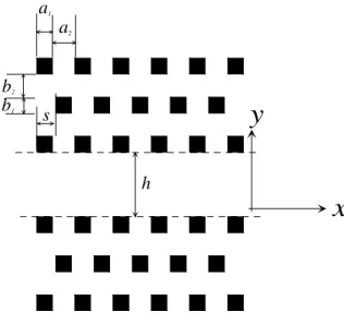
Figure 1 shows a stack of a finite number of identical, equal spaced, periodic layers of infinite extent on the horizontal plane. Each periodic layer is composed of an infinite number of rectangular dielectric rods of infinite length. When the number of the periodic layers in the stack is increased indefinitely, the structure can be viewed as an unbounded 2D periodic medium. Therefore, we may infer the propagation characteristics of the 2D periodic medium by the scattering characteristics of a stack of sufficiently large number of 1D periodic layers. With the coordinate system attached, the dielectric rods in each layer has the width a1 and the distance between
two neighboring rods is a2, thus the period of the layer is a = a1 + a2. For simplicity, a1/a is referred to as the aspect ratio of the 1D periodic layer. The thickness of each
1D periodic layer is b1 and the separation between two neighboring ones is b2. In
general, we assume that between two neighboring layers, there is a position shift of the distance s in lateral direction, so that we may investigate the effect of a large class of array patterns on the propagation characteristics of 2D periodic structures by adjusting the parameter s in our analysis. For example, we have a square array pattern for s = 0 and a triangular array pattern for s = 0.5a. Notice that for an arbitrary value of s, b = b1 + b2 is not necessary the period of the structure in the
y-direction. Actually, the structure has a period s2 +b2 along the direction at the
angle θ = sin-1(s/b) from the y-axis. Even though, the ratio b1/ b is referred to as the
aspect ratio in the y-direction.
f igure 1: Structural conf iguration of waveguide with 2D periodic walls of f inite thickness
a1 a2 b1 b2 s h
x
y
3. Mathematical AnalysisReferring to Figure 1, the 2D periodic structure consists of a finite number of 1D periodic layers, and scattering of plane waves by such a structure can be easily analyzed as a rigorous multilayer boundary-value problem. The formulation of such a type of boundary-value problems can be carried out for any values of s and it is
convenient for the analysis of the effect of array pattern on the propagation characteristics of the 2D periodic structures. For simplicity, this will be referred to as the scattering approach.
As will be explained in the next section, the scattering of plane-wave by a stack of 1D periodic layers can be analyzed in terms of that by a single 1D periodic layer. The scattering of plane-wave by a single 1D periodic layer has been well treated [16-20]. The formulation of the boundary-value problem is generally valid for any periodic profiles, as long as the characteristic solutions of the periodic medium can be constructed. For brevity, the input-output relation for a 1D periodic layer is outlined in this section while the detail derivation is referred to [19]. In this section, the results in the form of input impedance and transfer matrices will be used as a building block to analyze the plane-wave scattering by a stack of periodic layers.
A. Input-output relation of 1D periodic layer
For a 1D periodic layer, it is vertically uniform and is characterized by the relative dielectric constant: ) ( ) (x =ε x+d ε (1)
where d is the period. Due to the spatial periodicity in the x direction, a set of
Fourier components or space harmonics is generated everywhere in the structure. The propagation constant of the nth space harmonic in the x- direction is given by:
2 for ...,-2,-1,0,1,2,..., xn x k k n n d π = + = (2)
where kx is the wavenumber along the x-direction. According to the Floquet’s
theorem, the general field solutions can be expressed as a superposition of the complete set of space harmonics. The general electric and magnetic field solutions in 1D periodic medium can be written as follows [16]:
[
j z c j z d]
z Et( )=Qexp(− K ) +exp(+ K ) (3)[
j z c j z d]
z Ht( )=Pexp(− K ) −exp(+ K ) (4)where the tangential electric and magnetic field components are vectors with the amplitudes of space harmonics being their elements. Matrices P and Q are the coupling matrices with elements dependent on the structural parameters and the incident condition. K is the diagonal matrix with the propagation constant along the z-direction, kzm, as the mth diagonal element.
By imposing the boundary conditions at the interfaces between periodic and uniform layers, we can obtain the input-output relations of the periodic layer. The detail mathematical derivations can be found in reference [2]. The results are listed below. 1 1 ) )( ( + − − − =Q I Γ I Γ P Zin l l (5a)
exp(Γl = −j tK Γ) outexp(−j tK (5b) )
1
) )(
( + − −
= Z P Q Z P Q
Γout out out (5c)
1 ) )( ( + − − = Z P Q Z P Q T out out (5d)
matrices looking downward from the lower- and upper- surfaces of such 1D periodic layer, respectively, whereas T is the transfer matrix, which defines the transformation relation of the electric fields between the input and output interfaces. It is noted that the uniform layer can be regarded as the limiting case of 1D periodic layer with the vanishment of the periodic variations. In view of this, the input-output relation of the uniform layer will remain almost the same form but with slight modification and could be derived without any difficulties.
B. Scattering characteristics of the stack of 1D periodic layers
Underlying the input-output relation and transfer matrix for a single periodic layer as previously described, we can successively employ the input-output relation from the bottom- to the top- layer. Thus we can obtain the input impedance matrix looking downward from the top surface of the structure Zdn, the relationship between the
tangential electric and magnetic field vectors at the reference plane z = 0 can be
written as: ) 0 ( ) 0 ( dn t t H E =Z (6)
Meanwhile, the tangential electric and magnetic field vectors in the incident region (e.g. air), can be written as:
) ( ) 0 ( a b Et =Za + (7a) b a Ht(0)= − (7b)
where the vector a and b represent the incident and reflected plane waves. Since the tangential field components must be continuous at the interface at z = 0, we obtain a reflection matrix defining the relationship between incident and reflected plane waves, as given below: a b=Γ (8a) ) ( ) (Za Zdn 1 Zdn Za Γ= + − − (8b) where ΓΓΓΓ is the reflection matrix. After determining the reflection matrix, we obtain
the reflected amplitude associated with each space harmonic. Meanwhile, we also obtain the tangential electric and magnetic field over the input surface by equation 7(a). Furthermore, we successively employ the transfer matrix of 1D periodic and uniform layers, equation 5(d), from the top- to bottom- layer. Thus we can obtain the electric and magnetic field everywhere within the structure under consideration.
C. Guiding characteristics of the stacks of 1D periodic layers
The condition for the existence of nontrivial solutions in the absence of any incident wave leads to the vanishment of the coefficient matrix. It is so called the transverse resonance condition that defines the dispersion relation of the waveguide:
0 )
det(Za +Zdn = (9)
This equation defines the dispersion relation that determines the guided modes of the waveguide. The dispersion relation in equation (9) is a determinantal equation of infinite order; it requires a suitable truncation to a finite order to yield numerical
results. We have implemented a computer code on the basis of the exact formulation described above to determine the dispersion roots of the waveguide. The results are obtained systematically for various structural and incident parameters, thus we can identify the wave propagation phenomena and their physical implications.
4. Numerical Results and Discussions
According to the exact formulation described in the preceding section, we are now in a position to carry out both qualitative and quantitative analyses of guiding characteristics in such a class of waveguides. First, we shall invoke the concept of parallel-plate waveguide to model the waves propagating inside the waveguide. This allows us to identify the guiding characteristics of the waveguide in an easy manner for various physical effects associated with the structure and will be particularly useful for practical considerations. Second, for the numerical analysis, the infinite system equations for the Fourier amplitude have to be truncated to a finite order and the numerical accuracy has to be carefully studied. Note that it is essential to utilize some techniques to accelerate the convergence rate of the numerical process. After the numerical accuracy is assured, extensive numerical data are obtained to identify systematically all possible physical processes associated with the structure under consideration and to explore promising applications.
The characteristic solutions of the class of 2D periodic dielectric array certainly depend on the composition of the structure. The dielectric rods may have any cross-sectional shape and may be arranged in diverse array patterns. The relative dielectric constants of the dielectric rod and the surrounding medium are 11.4 and 1.0, respectively. The values of aspect ratio along x and y directions are 0.4 and 0.6, respectively. By a proper choice of the parameters a1, a2, b1, b2 and s, we can
generate any array patterns. For example, we can have a square pattern as we set a1
= a2 = b1 = b2 and the shift distance in the lateral direction s = 0; another case is the
triangular pattern in which the structural parameters remain unchanged as those of the square one while the lateral shift distance is changed to a half of the period along the x direction.
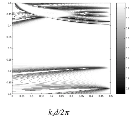
Contour of constant reflection coefficient
Since the reflection of plane wave by 2D periodic dielectric array depends on the angle as well as frequency of the incident plane wave, we have plotted the contour maps of constant reflection coefficient according to these two parameters. These contour plots provide a simple and useful procedure for the design of the waveguide for a desired number of propagating modes.
Figure 2 shows the contour plot of constant reflection coefficient for the finite stack of 1D periodic layers. The horizontal axis represents the normalized phase constant along x direction (i.e. kxd/2π ) and the vertical axis is the normalized frequency, d/λ. The reflectivity is plotted in gray-scale color map according to the level shown in the color bar on the right hand side of the figure. The region drawn in white color indicates the total reflection, that is, the reflection coefficient is close to unity. For instance, the band characterized by the normalized frequency (d/λ) 0.25-0.4 and the normalized phase constant 0-0.5 locates in the region of total reflection. Here, we can utilize the characteristics of total reflection in such region to serve as a waveguide wall and, as the waves bounce between the two walls so the electromagnetic energy flows along this guiding structure.
0.1 0.2 0.3 0.4 0.5 0.6 0.7 0.8 0.9 0 0.05 0.1 0.15 0.2 0.25 0.3 0.35 0.4 0.45 0.5 0.1 0.15 0.2 0.25 0.3 0.35 0.4 0.45 0.5
Dispersion characteristics of waveguide
Before embarking on an elaborate numerical analysis, it is instructive to consider first the approximation by the dispersion relation of an ideal parallel-plate waveguide. The dispersion relation of a parallel-plate waveguide with a separation h between the two metal plates can be expressed explicitly as:
a x d h nd d k ε λ π 2 2 2 2 2 = + (10)
where d is the period of 1D periodic layer along x direction, n is the mode index of the parallel-plate waveguide. This simple expression can be plotted graphically into curve in the form of Brillouin diagram, and the results are shown in dash line depicted in figure 3(a). The above equation determines a parabolic curve with the normalized cutoff frequency located at d/λ =d/2h , for the lowest order mode of the parallel-plate waveguide with TE polarization. In order to obtain a waveguide having the guiding characteristics as that of ideal parallel-plate waveguide, we should have the reflection characteristics of waveguide walls to be close to total reflection. In comparison with the contour map as shown in figure 2, we choose the cutoff condition: d/2h = 0.3 in order to assure that the dispersion curve is located in such region with strong reflection.
k
xd/2
π
d/
λ
Figure 2: Contour of constant reflection coefficient for the stacks of 1D periodic layer, where the number of stack is three.
According to the exact dispersion relation in (10), we have carried out a systematic evaluation of the guiding characteristics of the waveguide walls with the square pattern, and the results are displayed in the form of Brillouin diagram in figure 3(a) and (b) for both real and imaginary parts of kx. Note that the line in long dash is the
boundary of bound-wave region. The curves on the left-hand side of bound-wave boundary represent fast waves. From figure 3(a) we observe that the variation of phase constant for such a waveguide is very similar to that of ideal parallel-plate waveguide. Thus it can be concluded that the guiding characteristics of such waveguide are equivalent to those of parallel-plate waveguide. Another interesting observation is that, though we designed three cases with three, four and five 1D periodic layers as their waveguide walls; however, we can observe that the increase in the number of 1D periodic layers has a negligible effect on the phase constant. On the contrary, it reduces appreciably the attenuation due to the leakage of energy as depicted in figure 3(b). 0 0.1 0.2 0.3 0.4
β
xd/ 2
π
0 0.05 0.1 0.15 0.2 0.25 0.3 0.35 0.4d/
λ
a1a2 b1 b2 h x z ideal ppwgf igure 3(a): Variation of the phase constant versus normalized f requency f or dif f erent number of 1D periodic layers
0.2 0.24 0.28 0.32 0.36 0.4
d/
λ
1e-007 1e-006 1e-005 0.0001 0.001 0.01 0.1 1α
xd/
2
π
1e-007 1e-006 1e-005 0.0001 0.001 0.01 0.1 1 0.2 0.24 0.28 0.32 0.36 0.4 N=3 N=4 N=5 a1a2 b1 b2 h x z εs=11.4f igure 3(b): Variation of the attenuation constant versus normalized f requency f or dif f erent number of 1D periodic layers
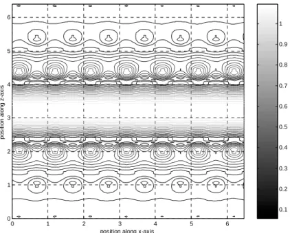
Field contour plot
To substantiate the guiding characteristics of waveguide modes in such a waveguide, we plot the contour of electric field component for understanding more easily of the physical picture of waveguiding in this waveguide. First, we randomly choose one point (d/2h = 0.3175) on the dispersion curve to plot the field distribution. Figure 4(a) is the distributions of field component Ey over the waveguide with square wall
pattern. Referring to the color bar attached, figure 4(a) indicates that the electric field is concentrated in the waveguide region and exhibits the localization of power within it. Away from this region, the field is exponentially decaying along the transverse direction.
0.1 0.2 0.3 0.4 0.5 0.6 0.7 0.8 0.9 1 0 0.5 1 1.5 2 2.5 3 3.5 4 4.5 5 0 1 2 3 4 5 6
position along x-axis
po s it ion a long z -ax is
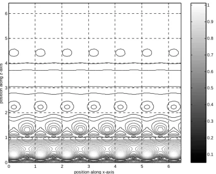
Distribution of Poynting vector
In addition to the field contour plots as shown previously, Poynting vector can also provide us some information about the power flow in waveguide. We setup a grid with considerable points in the structure and determine the vector Poynting power at each of those grid points. The resulting pattern is shown in figure 4(b) with the same parameters as that in figure 4(a). As we have known before, the real part of Poynting vector represents the magnitude and direction of power flow. In figure 4(b), the distribution of Poynting power is seen to be almost uniform in the central region and flows along the waveguide direction. On the other hand, the power leakage is negligible away from the waveguide, consistent with the fact that the attenuation constant is quite small.
Figure 4(a): Distribution of electric field components Ey(x,z) within the
waveguide with 2D periodic walls, which is arranged in square pattern; guiding analysis
0.5 1 1.5 2 2.5 1.5 2 2.5 3 3.5 4 4.5 5
position along x-axis
po s it ion a long z -ax is
Influence of the periodic pattern for the waveguide walls
Aside from studying the square pattern, we have also investigated the dispersion relation for various periodic patterns with different values of lateral shift distance s, for example, s ranges from zero to half of the period along x direction. Though not shown, we have found that the distribution for the phase constant almost converges to the same one. On the contrary, there are some differences between the attenuation constants. As shown in figure 5, we can take the attenuation constants of square and triangular pattern as upper and lower bounds, respectively. The lateral shift distance
s runs from 0.1 to 0.4 is located in the region. It is interesting to note that the
attenuation constant decreases as the increase in the shift distance. From the results we can conclude that the triangular pattern provide better stop band behavior than that of the other patterns. This permits us to design a low-loss waveguide by using the waveguide walls with triangular pattern.
Figure 4(b): Distribution of Poynting vector within the waveguide with 2D periodic walls, which is arranged in square pattern; guiding analysis
0.3 0.31 0.32 0.33 0.34 0.35 0.36 0.37 0.38
d/
λ
1e-008 1e-007 1e-006 1e-005 0.0001 0.001 0.01α
xd/
2
π
shift distance s=0 s=0.1 s=0.2 s=0.3 s=0.4 s=0.5 a1 a2 b1 b2 s h x yf igure 5: Variation of the attenuation constant versus normalized f requency f or various lattice pattern
Anomalous coupling between incident plane wave and localized modes in the waveguide
We have carried out considerable numerical experiments with various incident conditions and structure parameters; however, only a few sets are selected here to present the interesting phenomena that take place in the presence of 2D periodic structure. Figure 6(a) shows the reflection intensity of space harmonic n = 0 versus wavelength of the plane wave for various incident angles. Furthermore, we observe that there exists a sharp variation along each curve, as marked by the characters from A’ to E’ in figure 6(a).
0.28 0.29 0.3 0.31 0.32 0.33 0.34 0.35 0.36 0.37 0.38 0.39 0.4
d/
λ
0 0.1 0.2 0.3 0.4 0.5 0.6 0.7 0.8 0.9 1 Di ff rac tion E ff ic ienc y o f ze ro-th o rd er 0.28 0.29 0.3 0.31 0.32 0.33 0.34 0.35 0.36 0.37 0.38 0.39 0.4 0 0.1 0.2 0.3 0.4 0.5 0.6 0.7 0.8 0.9 1 A' B' C' D' E' a1 a2 b1 b2 s h x z θincf igure 6(a): Variation of the ref lection intensity versus normalized f requency f or various incident angles; the number of 1D periodic layer is three and is arranged in triangular pattern
To explain the unusual behavior of reflection characteristics, we recall the dispersion curve of a waveguide with 2D periodic walls of triangular pattern. Referring to the inset in figure 6(b), a plane wave of TE polarization is incident on the waveguide at an angle θinc with respect to z axis. The phase constant kx along the x direction is
given by:
inc o
x k
k = sinθ (11)
where ko is the free-space wavenumber.
For a given incident angle θinc, the relationship between kxd/2π and kod/2π can be
represented as a straight line passing through the origin with the slope 1/sinθinc.
Here, we plot the straight line for various angles together with Brillouin diagram in figure 6(b). Note that the two extreme cases: θinc = 0o and θinc = 90o, of incident
angles correspond to the left vertical axis and the boundary of bound-wave region with the slope equal to unity, respectively.
0 0.1 0.2 0.3 0.4
β
xd/ 2π
0 0.05 0.1 0.15 0.2 0.25 0.3 0.35 0.4d/
λ
30o 45 o A B 20o 55o 10o C D Ef igure 6(b): Variation of the phase constant versus normalized f requency f or dif f erent number of 1D periodic
layers which is arranged in triangular pattern
θinc a1 a2 b1 b2 s h
The intersection points between incident plane wave and waveguide mode are circled and labeled in alphabetical order for various incident angles, as shown in figure 6(b). Each of the intersection points represents a case of strong coupling in which the real part of the guided-wave wavenumber along the x direction is the same as that of the incident plane wave. Over the frequency range covering each set of intersection points, we calculate the reflected power under the same incident conditions. The variation of reflected power versus normalized frequency is shown in figure 6(a). Returning to figure 6(a), we observe the sharp decreases in the bandwidth at different frequencies as marked by the characters A’, B’, C’, D’ and E’, respectively. Comparing to figure 6(b), we found that the position of rapid variation corresponds to the intersection points A, B, C, D and E, respectively. It is interesting to note that at these intersection points there are very small attenuation constants for the waveguide, as shown in figure 6(c). Thus good phase-matching condition occurs at these points and strong coupling takes place between the incident plane wave and the waveguide mode supported by this structure. Particularly, the attenuation constants are very close to zero at the intersection points C and D, hence the coupling takes place almost at certain frequencies, as shown in this figure.
0.2 0.22 0.24 0.26 0.28 0.3 0.32 0.34 0.36 0.38
d/
λ
1e-007 1e-006 1e-005 0.0001 0.001 0.01 0.1α
xd/
2
π
0.2 0.22 0.24 0.26 0.28 0.3 0.32 0.34 0.36 0.38 1e-007 1e-006 1e-005 0.0001 0.001 0.01 0.1 N=3 N=4 N=5 a1 a2 b1 b2 s h x yf igure 6(c): Variation of the attenuation constant versus normalized f requency f or dif f erent number of 1D periodic
layers which is arranged in triangular pattern
To verify the anomalous coupling due to phase-matching condition, we also plot the contour plots for the electric and magnetic field components, as we have done in the previous example. In this example, the incident angle is designated as 30o and the normalized frequency is d/λ = 0.317, which is also the case characterized by the conditions at the intersection point C. We can observe that the field component
Ey(x,z), as depicted in figure 7, has almost the identical pattern as shown in figure 4(a).
Thus we can infer that the incident plane wave will couple its energy into such waveguide at the phase-matching condition, which is also known as a anomalous coupling between the incident plane wave and the waveguide mode supported by the waveguide.
0.1 0.2 0.3 0.4 0.5 0.6 0.7 0.8 0.9 1 0 1 2 3 4 5 6 0 1 2 3 4 5 6
position along x-axis
po s it ion a long z -ax is
Also, addition to the phase-matching condition, in this example, we choose an incident condition away from the point of phase-matching condition such as θinc = 30o
and d/λ = 0.35, for example, to study the scattering characteristics. Since the phase of incident plane wave can’t match with that of guided mode supported by the structure, the incident power can’t couple into the waveguide and is reflected back to the free-space. The contour plot of field component Ey(x,z) and the distribution of
Poynting vector are shown figure 8(a) and 8(b), which indicate that the incident plane wave is reflected by the structure and can hardly penetrate into the structure any further.
Figure 7: Distribution of electric field components, Ey(x,z), within the
waveguide with 2D periodic walls, which is arranged in triangular pattern; scattering analysis
0.1 0.2 0.3 0.4 0.5 0.6 0.7 0.8 0.9 1 0 1 2 3 4 5 6 0 1 2 3 4 5 6
position along x-axis
po s it ion a long z -ax is 0.5 1 1.5 2 2.5 3 3.5 4 0 0.5 1 1.5 2 2.5 3 3.5 4
position along x-axis
po s it ion a long z -ax is
Figure 9 shows the contour plot of constant reflection coefficient for the waveguide with triangular wall pattern. In this example, we plot the map versus both
Figure 8(a): Distribution of electric field components Ey(x,z) within the
waveguide with 2D periodic walls, which is arranged in triangular pattern; scattering analysis
Figure 8(b): Distribution of Poynting vector within the waveguide with 2D periodic walls, which is arranged in square pattern;
normalized frequency and phase constant along x direction. It is interesting to note that there exists some points with low reflectivity arranged along a parabolic curve, which is the same as shown in figure 6(b). As we have known previously these points are based on the presence of anomalous coupling (phase-matching condition). Therefore, as long as the attenuation constant of waveguide mode is not quite obvious, the phase constant of the waveguide mode must be predicted by the phase-matching condition by means of the scattering analysis. In a word, we can infer that the guiding characteristic of the waveguide through its scattering characteristic, in particular, by means of the presence of anomalous coupling (phase-matching condition). 0.3 0.4 0.5 0.6 0.7 0.8 0.9 1 0 0.05 0.1 0.15 0.2 0.25 0.3 0.35 0.4 0.45 0.5 0.1 0.15 0.2 0.25 0.3 0.35 0.4 0.45 0.5 5. Conclusions
We have employed the rigorous mode-matching method to deal with the problem of scattering and guiding characteristics of waveguide with 2D periodic walls of finite thickness. The scattering characteristics of 2D periodic dielectric array utilized as a waveguide wall have been analyzed first to realize its stop band behavior. And then the guiding characteristics of waveguide using such a class of 2D periodic walls are studied in detail. Extensive numerical results have been obtained to examine the guiding phenomena of the waveguide together with different array patterns. In
d/
λ
Figure 9: Contour plot of constant reflection coefficient within the waveguide with 2D periodic walls, which is arranged in square pattern; scattering analysis.
addition, an anomalous coupling between incident plane wave and the waveguide modes has also been investigated and was utilized for the first time to predict the guiding characteristic of the waveguide.
Acknowledge
This author would like to thank Prof. S. T. Peng and Prof. F. Y. Chang, Chiao-Tung University, Taiwan, R.O.C for their encouragement, constructive criticism and many suggestions for improvement. This research work was supported by the Ministry of Education and National Science Council.
References
1. H. Y. David Yang, “Finite Difference Analysis of 2-D Photonic Crystals,” IEEE
Trans, Microwave Theory Tech., vol. 44, no.12, Dec. 1996.
2. G. P. Gauthier, A. Courtay, and G. M. Rebeiz, “Microstrip antennas on synthesized low dielectric-constant substrates.” IEEE Trans. Antennas Propagat. Vol. 45. Pp. 1310-1314. Aug. 1997.
3. Papapolymerou, R. F. Drayton, and L. P. B. Katechi. “Micromachined patch
antennas.” IEEE Trand. Antennas Propagat. Vol. 46. Pp.275-283. Feb. 1998.
4. V. M. Lubecke. K. Mizuno. And G. M. Rebeiz. “Micromachining for terahertz applications.” IEEE Trans. Microwave Theory Tech. Vol. 46. Pp 1821-1831. Nov. 1998.
5. Dan Sievenpiper, Lijun Zhang, Romulo F. Jimenez Broas, Nicholas G. Alexopolous,and Eli Yablonovitch. “High-Impedance Electromagnetic Surface with a Forbidden Frequency Band.” IEEE Trans. Microwave Theory tech. Vol. 47. pp 2059-2074. Nov. 1999.
6. Fei-Ran Yang, Kuang-Ping Ma, Yongxi Qian,and Tatsuo Itoh, “A Novel TEM Waveguide Using Uniplanar Compact Photonic-Bandgap(UC-PBG) Structure.”
IEEE Trans. Microwave Theory tech. Vol. 47. pp 2092-2098.
7. R. B. Hwang and S. T. Peng, “Guidance Characteristics of Two-Dimensional Periodic Impedance Surface”, IEEE Transaction on Microwave Theory and
Techniques, Vol. 47, No. 12, pp. 2503-2511, December, 1999.
8. R. B. Hwang and S. T. Peng, “Guided waves on 2D Periodic Structures and their Relation to Planar Photonic Band Gap structures”, Accepted for publication in
IEICE Transactions on Electronics, 1999
9. Attila Mekis, Shanhui Fan, and J. D. Joannopoulos, “Absorbing boundary conditions for FDTD simulations of photonic crystal waveguides”, IEEE Microwave and Guided Wave Letters, Vol. 9, No. 12, pp502-504, December 1999. 10. D. Maystre, “Electromagnetic study of photonic band gaps,” Pure Appl. Opt.,
vol.3, no.6, pp.975-993, Nov. 1994.
11. J. D. Joannopoulos, R. D. Meade, and J. N. Winn, Photonic Crystal: Modeling the flow of light. Princeton, NJ: Princeton University Press, 1995.
12. E. Noponen and J. Turunen, “Eigenmode method for electromagnetic synthesis of diffractive elements with three-dimensional profiles,” J. Opt. Soc. Am. A, vol. 11, no. 9, 2494-2502, 1994.
13. Vardaxoglou, J.C.; Hossainzadeh, A.; Stylianou, A. “Scattering from two-layer FSS with dissimilar lattice geometries,” Microwaves, Antennas and Propagation, IEE Proceedings H Volume: 140 1 , Feb. 1993 , Page(s): 59 -61
1967 G-MTT International Microwave Symposium Program and Digest, pp. 17-22.
15. R. B. Hwang and S. T. Peng, ”Properties of Waveguides with Periodic Side Walls of Finite Width”, Progress in Electromagnetic Research, 2002 Nov. 1999.
16. S. T. Peng, "Rigorous formulation of scattering and guidance by dielectric grating waveguides: general case of oblique incidence," J. Opt. Soc. Am. Vol. 6, 1869-1883 (1989).
17. T. Tamir, H. C. Wang and A. A. Oliner, “Wave Propagation in sinusoidally Stratified Dielectric Media,: IEEE Trans. MTT, vol.MTT-12, p.323, 1964.
18. A. Hessel and A. A. Oliner, “A New Theory of Wood’s Anomalies on Optical Gratings,” Appl. Optics, Vol.4, 1275-1297, (1965).
19. S. T. Peng, T. Tamir and H.L. Bertoni, “Theory of dielectric grating waveguides,” IEEE Trans. MTT, Vol. MTT-23, p123-133, 1975.
20. R. C. Hall, R. Mittra and K.M. Mitzner, “Analysis of multilayered periodic structures using generalized scattering matrix theory,” IEEE Trans. Antenna and Propagation, vol.36, no.4, 511-517.