Comparison of oxide breakdown progression in ultra-thin oxide silicon-on-insulator
and bulk metal-oxide-semiconductor field effect transistors
M. C. Chen, S. H. Ku, C. T. Chan, and Tahui Wang
Citation: Journal of Applied Physics 96, 3473 (2004); doi: 10.1063/1.1776640 View online: http://dx.doi.org/10.1063/1.1776640
View Table of Contents: http://scitation.aip.org/content/aip/journal/jap/96/6?ver=pdfcov Published by the AIP Publishing
Articles you may be interested in
Tunneling spectroscopy of electron subbands in thin silicon-on-insulator metal-oxide-semiconductor field-effect transistors
Appl. Phys. Lett. 96, 112102 (2010); 10.1063/1.3360224
Soft breakdown enhanced hysteresis effects in ultrathin oxide silicon-on-insulator metal-oxide-semiconductor field effect transistors
J. Appl. Phys. 96, 2297 (2004); 10.1063/1.1773384
Enhanced electroluminescence in silicon-on-insulator metal–oxide–semiconductor transistors with thin silicon layer
Appl. Phys. Lett. 82, 4830 (2003); 10.1063/1.1587877
Low-frequency noise overshoot in ultrathin gate oxide silicon-on-insulator metal–oxide–semiconductor field-effect transistors
Appl. Phys. Lett. 82, 1790 (2003); 10.1063/1.1561575
Nitrided thermal SiO 2 for use as top and bottom gate insulators in self-aligned double gate silicon-on-insulator metal–oxide–semiconductor field effect transistor
J. Vac. Sci. Technol. B 19, 800 (2001); 10.1116/1.1364698
enhanced progression is attributed to the increase of hole stress current resulting from breakdown induced channel carrier heating in a floating-body configuration. Numerical analysis of hole tunneling current and hot carrier luminescence measurement are performed to support our proposed theory. This phenomenon is particularly significant to the reliability of devices with ultra-thin oxides and low operation gate voltage. © 2004 American Institute of Physics.[DOI: 10.1063/1.1776640]
I. INTRODUCTION
The aggressive scaling of advanced complementary metal-oxide-semiconductor (CMOS) field effect transistors
(MOSFETs) has pushed the gate oxide thickness towards its
limit in terms of reliability.1–4 In ultra-thin gate oxide MOSFETs, oxide breakdown(BD) has been shown to evolve in a continuous manner from initial stages to final shorting.5–7Previous study has shown that a small increase in gate leakage due to oxide BD does not disrupt circuit opera-tion, and the failure criterion should be changed to a higher level of gate leakage.8,9Therefore, the oxide failure time is determined by BD hardness involved in a progressive pro-cess, or in other words, by BD evolution rate. Presently, the silicon-on-insulator (SOI) technology has emerged to be a candidate for advanced CMOS technology for its higher per-formance. The BD progression in conventional bulk CMOS devices10–12 has been widely investigated. In this paper, we will investigate the influence of floating body effect on BD progression in partially depleted(PD) p-type SOI MOSFETs. Several concerns of hard breakdown evolution in ultra-thin oxides have been proposed.7–14Monsieur et al.7reported that for low gate stress bias, the defect generation rate being very low, the degradation of the BD conduction path be-comes macroscopic and can last thousands of seconds even in the case of accelerated test. Linder et al.9showed that the growth of BD current could be exponentially dependent on gate bias, oxide thickness, and any other parasitics, such as inversion layer resistances, altering the observed growth rate drastically. Alam et al.13indicated that circuits do continue to operate after the first soft breakdown(SBD), and suggested that the standard reliability specification is too restrictive, and should be redefined, particularly for pMOS devices. In ultra-thin oxide pMOSFETs, enhanced gate oxide BD growth rate was observed with a negative substrate bias.14 Further-more, the floating body configuration of partially depleted SOI CMOS may result in a nonzero body voltage due to various body charging mechanisms15–18and thus affects
ox-ide BD evolution. The objective of this paper is therefore to investigate floating body effect on BD progression rate. A model based on breakdown induced channel carrier heating will be proposed to explain the observed phenomenon.
II. DEVICES AND EXPERIMENT
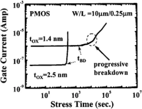
The devices in this work were made with an optimized 0.13m CMOS process on p-type SOI wafer and have a gate length of 0.5m, a gate width of 2m, and an oxide thickness of 1.6 nm. The gate oxide was grown with rapid plasma nitridation process. The test devices have an H-gate structure with an additional contact to facilitate the measure-ment of the body current and voltage. In this paper, all de-vices were stressed at constant gate voltage with the source and drain grounded. Figure 1 shows typical BD evolution in a 1.4 nm oxide and a 2.5 nm oxide bulk pMOSFETs. In the 1.4 nm gate oxide pMOSFET, oxide BD is evolved in a pro-gressive way, and the gate leakage current increases gradu-ally with stress time. As a contrast, the 2.5 nm oxide pMOSFET exhibits an abrupt jump in gate leakage current after BD. Since a slight gate leakage increases due to oxide BD is considered to be nondestructive for circuit operation,8 we define oxide breakdown time tBDand device fail time tfail
a)Electronic mail: [email protected]
FIG. 1. Comparison of breakdown behavior in a 1.4 nm oxide pMOSFET and in a 2.5 nm oxide pMOSFET. The stress gate voltage is −3 V for the 1.4 nm oxide and −4.5 V for the 2.5 nm oxide. tBDdenotes the onset time of
oxide breakdown.
0021-8979/2004/96(6)/3473/5/$22.00 3473 © 2004 American Institute of Physics
as the time when the gate leakage current reaches 1.5 times and 15 times its prestress value, respectively.
III. RESULT AND DISCUSSION A. A shortertfailin SOI pMOSFETs
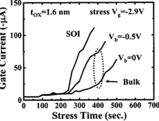
Figure 2 shows the gate leakage current evolution with stress time at a stress gate voltage of Vg= −2.9 V for various
applied substrate biases共Vb兲 in pMOSFETs. The oxide tBDis almost the same for different substrate biases. This can be understood because oxide defect generation rate is dependent on injected charge energy and fluence during stress,19–22 re-gardless of applied substrate bias. After the onset of BD, the BD growth rate exhibits an apparent dependence on substrate bias. A forward substrate bias can significantly enhance BD growth rate. It should be noted that the SOI device with floating-body configuration has the worst BD progression rate in Fig. 2. The statistic Weibull distributions of oxide tBD and tfailfor SOI(floating substrate) and bulk (grounded sub-strate) pMOSFETs are plotted in Fig. 3. Although the float-ing substrate configuration does not affect tBD, it does cause a two times shorter tfailthan in bulk pMOSFETs.
B. Mechanism of enhanced BD progression in SOI The floating body configuration of SOI devices may re-sult in a small forward body voltage due to various body
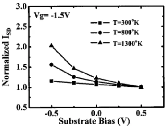
charging processes. In an ultra-thin oxide pMOSFET, the gate stress current may have comparable electron and hole components at a negative gate bias. To analyze the polarity of dominant stress current in a pMOSFET, a charge separa-tion technique is utilized to measure electron stress current and hole stress current. The inset of Fig. 4 illustrates the carrier flow at a negative gate bias, Ib denotes electron
cur-rent and comes from valance-band electron tunneling from the gate electrode. Isdstands for hole tunneling current from the inverted channel. The substrate bias dependence of elec-tron current and hole current before and after tBDis shown in Fig. 4. Note that the electron and hole currents in a fresh device are independent of substrate bias. Interestingly, the post-tBDhole current, unlike the pre-BD, Ib, and Isd, exhibits a significant Vbdependence. Furthermore, Fig. 5 reveals that
the Vbdependence of the post-tBDhole current increases with BD evolution. Since the hole stress current dominates gate stress during (BD) evolution and increases with a forward body bias, the enhanced(BD) progression in a floating body configuration can be understood.
C. BD caused carrier heating
Since the post-tBDelectron current does not exhibit Vb dependence (Fig. 4), the possibility that the Vb dependence of the post-tBD hole current is caused by the variation of effective gate-to-channel voltage resulting from Vb
modu-lated channel resistance can be excluded. Otherwise, the post-tBDIb should have the same Vb effect as the post-FIG. 2. Oxide breakdown progression in bulk and SOI pMOSFETs. The
stress gate bias is −2.9 V and temperature is 125° C.
FIG. 3. The Weibull plots of tBDand tfaildistribution for 1.6 nm oxide SOI
and bulk pMOSFETs. The stress gate bias is −2.9 V and the temperature is 125° C. tBDand tfailare defined as the time for gate current to reach 1.5 times
and 15 times its prestress value, respectively.
FIG. 4. The Vbdependence of pre-BD and post-BD electron currents Iband hole currents Isdat Vg= −1.5 V. Distinct Vbdependence of the post-tBDIsdis
noted. The floating body configuration corresponds to a body voltage of approximately −0.65 V. The inset illustrates carrier flow in a pMOSFET at a negative gate bias.
FIG. 5. The Vbdependence of the hole current Isdat different stress times,
t0,t1, t2, and t3. Isd is normalized to its value at Vb= 2 V. Gate current vs
stress time in a stress condition of Vg= −3.2 V and T = 25° C is shown in the inset.
3474 J. Appl. Phys., Vol. 96, No. 6, 15 September 2004 Chenet al.
tBDISD. Moreover, substrate impact ionization and negative bias-temperature instability effects are also excluded because the trend of the Vb dependence is opposite.
To further investigate the origin of the Vbdependence of the post-tBDhole current, we measured the spectral distribu-tion of hot carrier light emission before and after tBD(Fig. 6). The light intensity is greatly increased after oxide BD. The high-energy tail of the post-tBDspectral distribution indicates the rise of the carrier temperature. Similar finding was also reported by other groups.23The extracted carrier temperature from the high-energy tail of the spectrum is around 1300 K
[Fig. 6(b)]. There are two possible theories to explain the rise
of channel carrier temperature at a BD spot. First, based on the model proposed by Rasras et al.,23the gate voltage may penetrate into the substrate after BD and causes lateral field heating of channel carriers. However, this process is unlikely here since the post-tBDelectron current and hole current have distinctly different Vbdependence. The second possible
rea-son is that high-dissipated energy, released by valence elec-trons tunneling from the gate through the BD path, will lo-cally produce a rise of hole temperature. A temperature range of 1000 to 2000 K was estimated in Ref. 24. Electron-hole scattering or Auger recombination is suspected to be the re-sponsible energy transfer process.
To show that the rise of hole temperature may account for the observed Vb dependence, we calculate the hole
tun-neling current with hole temperature at 300 K and 1300 K. In our calculation, we solve the coupled Poisson and Schrödinger equations to obtain the subband structure for the inversion holes (Fig. 7). A simple one-band effective mass approximation is used for simplicity. The hole tunneling cur-rent is calculated according to the Tsu-Esaki formula25
Isd= qm储ⴱ
冉
122ប3
冊
kBT兺
n Dn„ln兵1 + exp关共En− Ef兲/kBT兴其 − ln兵1 + exp关共En− Ef⬘兲/kBT兴其…, 共1兲where Ef共Ef⬘兲 denotes the Fermi energy in the channel (poly gate) and Dn is the hole tunneling probability of the nth subband. mⴱis the hole effective mass in Si. Other variables have their usual definitions. It should be emphasized that it is not our intention to consider detailed trap-assisted charge transport in the BD path. It is also not our intension to cal-culate the precise current value before and after oxide BD, since the BD area and BD caused effective oxide thinning cannot be easily determined. Instead, our purpose is to inves-tigate the effect of hole temperature on the inversion hole distribution in different subbands and the corresponding sub-strate bias effect on hole tunneling current. Therefore, a simple WKB formula for direct tunneling is employed for
Dn.
Our result in Fig. 8 clearly shows that the hole tunneling current exhibits a larger Vbdependence at 1300 K. The
simu-lation can well interpret the measured Vbdependence of the TABLE I. Calculated distribution of channel holes in the lowest three sub-bands. The gate bias in simulation is −1.5 V. The parameters used in simu-lation is mⴱ共Si兲=0.67 m0, mⴱ共SiO2兲=0.55 m0,h (hole barrier height at SiO2 interface)=4.25 eV, tox= 1.6 nm, and NB (substrate doping)=1
⫻1018cm−3.
Channel hole dist.(%)
300 K 1300 K
Subband Vb= −0.5 Vb= 2 Vb= −0.5 Vb= 2
1st 96.6 99.5 39.8 99.4
2nd 3 0.5 18 0.6
3rd 0.3 0 11.6 0
FIG. 7. Illustration of hole distribution in subands at a hole temperature of 300 K and 1300 K. Higher carrier temperature results in a larger Vbeffect.
FIG. 8. Simulated substrate bias effect on hole tunneling current in a 1.6 nm oxide pMOSFET. Isdis normalized to its value at Vb= 2 V. Simulated Vg
= −1.5 V. FIG. 6. Spectral distribution of light emission in a 1.4 nm oxide pMOSFET
at Vg= −2.5 V. The extracted carrier temperature from the high-energy tail of the spectrum is around 1300 K.
post-tBD Isd by simply using an elevated hole temperature. The trend in Fig. 8 is similar to the measured Vbdependence
in Fig. 5. To explain the temperature effect on the Vb
depen-dence in more detail, the distribution of inversion holes in the lowest three subbands is given in Table I. At T = 300 K, channel holes mostly reside in the first subband no matter of
Vb. At T = 1300 K, a large part of holes are thermally excited to higher subbands at a forward body voltage 共−0.5 V兲, where the oxide tunneling probability is larger. Thus, a much larger hole tunneling current is obtained at negative body voltages.
IV. THE IMPACT OF GATE STRESS BIAS
From previous discussion, the Vb dependence of hole stress current was identified to be the origin of the floating-body enhanced BD progression. Now, the impact of gate stress bias scaling on the enhanced BD progression is ex-plored. Figure 9 shows the Vbdependence of BD current at various measurement gate biases. The Vb dependence is
more distinguished at a smaller gate bias. Figure 10 shows the range of the gate stress bias where hole current is domi-nant. The hole current dominates gate stress at small gate biases (less than ⬃3.0 V) and the hole component of the stress current increases during BD evolution. This result is consistent with the findings in Fig. 9 that a large Vb
depen-dence of the post-BD stress current is obtained at smaller gate voltages. Figure 11 compares the 63% time-to-failure in
SOI and bulk pMOSFETs at various gate stress biases. Ac-celerated BD progression is noticed in SOI samples and the trend becomes more apparent at lower gate stress biases. Figure 12 shows the range of oxide thickness and stress gate voltage, where the hole current component is dominant in a fresh device and after breakdown. For example, for an oxide thickness of 1.6 nm, hole current is dominant in stress for
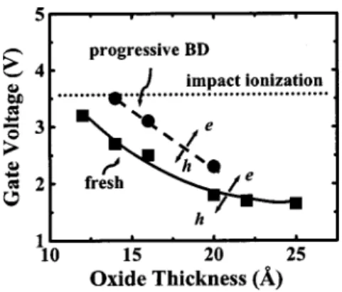
Vg⬍2.5 V in a fresh device and for Vg⬍3.0 V after BD.
High-energy electron impact ionization does not need to be considered until Vg is above 3.5 V. Figure 12 also reveals
that the hole current dominant region increases not only with BD progression but with decreasing oxide thickness. It im-plies that the floating body enhanced BD progression will become more significant as oxide thickness scales down.
V. CONCLUSION
In ultra-thin oxide SOI pMOSFETs, breakdown progres-sion is aggravated by a forward body bias. An enhanced post-tBDgate current is observed in SOI devices due to the charging of the floating body. Numerical analysis shows that the Vb enhanced hole stress current can be explained by the increase of hole temperature at the breakdown spot. The Vb
accelerated BD progression is more significant at a lower stress gate bias and for a thinner oxide.
FIG. 9. Substrate bias dependence of the post-BD hole current at various gate biases. Isdis normalized to its value at Vb= 2 V.
FIG. 10. Gate bias dependence of electron current and hole current in a fresh pMOSFET and during progressive BD.
FIG. 11. tfail共63%兲 vs gate stress bias for SOI and bulk pMOS devices.
FIG. 12. The range of oxide thickness and stress gate voltage, where the hole current component is dominant in a fresh device and after breakdown h or e represents hole current or electron current dominant regime, respectively.
3476 J. Appl. Phys., Vol. 96, No. 6, 15 September 2004 Chenet al.
4
E. Miranda, J. Sune, R. Rodriguez, M. Nafria, and X. Aymerich, Appl. Phys. Lett. 73, 490(1998).
5
T. Hosoi, P. L. Re, Y. Kamakura, and K. Taniguchi, Tech. Dig. - Int. Electron Devices Meet. 2002, 155.
6
B. P. Linder, S. Lombardo, J. Stathis, A. Vayshenker, and D. Frank, IEEE Electron Device Lett. 23, 661(2002).
7
F. Monsieur, E. Vincent, D. Roy, S. Bruyere, J. C. Vildeuil, G. Panan-akakis, and G. Ghibaudo, Proc. Int. Reliab. Phys. Symp. ,2002, p. 45.
8
B. Kaczer, R. Degraeve, G. Groeseneken, M. Rasras, S. Kubicek, E. Van-damme, and G. Badenes, Tech. Dig. - Int. Electron Devices Meet. 2000, 553.
9
B. P. Linder, J. H. Stathis, D. J. Frank, S. Lombardo, and A. Vayshenker, Proc. Int. Reliab. Phys. Symp. ,2003, p. 402.
17
T. Poiroux, O. Faynot, C. Tabone, H. Tigelaar, H. Mogul, N. Bresson, and S. Cristoloveanu, IEEE International SOI Conference(2002).
18
M. C. Chen et al., Proc. Int. Reliab. Phys. Symp. , 2002, p. 404.
19
J. S. Suehle, IEEE Trans. Electron Devices 49, 958(2002).
20
J. H. Stathis, J. Appl. Phys. 86, 5757(1999).
21
E. Miranda and J. Sune, Appl. Phys. Lett. 78, 225(2001).
22
R. Degraeve, G. Groeseneken, R. Bellens, J. L. Ogier, M. Depas, P. J. Roussel, and H. E. Maes, IEEE Trans. Electron Devices 45, 904(1998).
23
M. Rasras, I. De Wolf, G. Groeseneken, R. Degraeve, and H. E. Maes, Tech. Dig. - Int. Electron Devices Meet. 2000, 537.
24
S. Lombardo, A. La Magna, C. Spinella, C. Gerardi, and F. Crupi, J. Appl. Phys. 86, 6382(1999).
25
R. Tsu and L. Esaki, Appl. Phys. Lett. 22, 562(1973).