Enhanced Output Power of GaN-Based
Resonance Cavity Light-Emitting Diodes
With Optimized ITO Design
Tzeng-Tsong Wu, Chien-Chung Lin, Member, IEEE, Yun-Lin Wu, Chien-Kang Chen,
Tien-Chang Lu, Member, IEEE, Hao-Chung Kuo, Senior Member, IEEE, and
Shing-Chung Wang, Life Member, IEEE, Fellow, OSA
Abstract—We fabricated and measured GaN-based resonant
cavity light-emitting diodes with a 30 nm thick Indium tin oxide (ITO) thin film as a transparent contact layer. Four different ITO structures on p-type GaN samples were deposited by sputter and e-gun, and the corresponding device performance was compared. Each of these four samples has been annealed by its optimal parameters. The ITO thin film deposited by sputter demonstrated better electrical characteristics, surface morphology, specific contact resistance, and the overall device light output compared to those of the e-gun samples. Between the two sputtered ITO types, the hybrid type shows higher roll-over current density of 14 kA/cm , and the output power is increased from 15 to 39 W. From statistical data of the 2-D light intensity under the same cur-rent, we saw the lateral current spreading of the pure crystalline ITO by sputter is worst. The hybrid type, which combines the crystalline and amorphous ITO, has the best overall performance when we consider all the electrical, optical, and metrology mea-surements. From these results, we believe the 30 nm thick hybrid ITO thin film has the best potential to be applied in light emitting devices such as light-emitting diodes, laser diodes, etc.
Index Terms—Current spreading, GaN, indium tin oxide (ITO),
resonance cavity light-emitting diodes (RCLEDs).
I. INTRODUCTION
G
ALLIUM NITRIDE (GaN) is an attractive material due to its wide bandgap and its emission in blue-green wave-length which can be applied extensively in the optoelectronic devices including light emitting diodes (LEDs) and laser diodes Manuscript received August 10, 2011; revised October 12, 2011; accepted October 12, 2011. Date of publication October 19, 2011; date of current version December 14, 2011. This work was supported in part by the Ministry of Edu-cation Aim for the Top University program and in part by the National Science Council of Taiwan under Contract NSC 98-3114-E009-002-002, Contract NSC 98-3114-E009-009-001, and Contract NSC 98-2923-E009-001-MY3.T.-T. Wu, Y.-L. Wu, T.-C. Lu, H.-C. Kuo, and S.-C. Wang are with the Department of Photonics and Institute of Electro-Optical Engineering, Na-tional Chiao Tung University, Hsinchu 30050, Taiwan (e-mail: mulderbob. eo98g@nctu.edu.tw; hotcafe905@hotmail.com; timtclu@mail.nctu.edu.tw; hckuo@faculty.nctu.edu.tw; scwang@cc.nctu.edu.tw).
C.-K. Chen was with the Department of Photonics and Institute of Electro-Optical Engineering, National Chiao Tung University, Hsinchu 30050, Taiwan. He is now with AU Optronics Corporation, Science Park, Hsinchu 30078, Taiwan (e-mail: agonchen@msn.com).
C.-C. Lin is with the Institute of Photonics System, National Chiao Tung University, Tainan 711, Taiwan (e-mail: chienchunglin@faculty.nctu.edu.tw).
Color versions of one or more of the figures in this paper are available online at http://ieeexplore.ieee.org.
Digital Object Identifier 10.1109/JLT.2011.2172916
(LDs) [1]–[3]. To fabricate highly efficient optoelectronic de-vices, electrical contacts to GaN layers (n-type or p-type) play important roles. There are many methods to improve electrical characteristics of the GaN-based devices, such as choices of metal for a stable ohmic contact, a better current spreading layer design, and better epitaxial quality.
However, due to low doping density resulted from high acti-vation energy of the p-type dopant, the electrical conductance of p-GaN contact is worse than that of n-type GaN. Therefore, it is important to find a better conductive layer on p-GaN for current spreading. This layer should not only form good ohmic contacts to p-GaN, but also have higher transparency at emission wave-length. In the past few years, Ni/Au contact was widely used in commercial GaN-based LEDs. The specific contact resistance between p-GaN and metal contact can reach – cm after annealing. However, the Ni/Au layer has high absorption, and it was reported that the transmittance of Ni/Au only around 60–85% in the wavelength range from 450 to 550 nm [4]. The absorption of contact layer is particularly important for LEDs and LDs because it would decrease the output power. Nowa-days, indium tin oxide (ITO) has gradually replaced the con-ventional metal conductive layer such as Ni/Au due to its high transparency and its low electrical resistivity ( cm). So far, there have been many studies about the ITO thin film for op-toelectronic device application [5]–[8]. In general, ITO is a mix-ture material of indium oxide (In O ) and tin oxide (SnO ), and both of them have a wide bandgap ( eV) and low elec-trical resistivity ( cm). The oxygen vacancies accompanied with the Sn donor, which are responsible for its high conductivity, but can also lead to non-stoichiometric ITO. In the optical characteristics, ITO shows high absorption in the UV region, high transmittance % in the visible region, and high reflectance in the infrared (IR) region. In addition, the ITO thin film is thermally stable and has better device reliability compared to the Au-based contact. Due to these unique prop-erties, ITO has been used in a wide range application, such as transparent electrodes for display and solar cell [9], [10], IR re-flective mirrors for building and transparent conducting layers for nitride-based devices [11], [12].
Up to now, there are many methods applied in the deposition of ITO film such as sputter, e-gun evaporation [13], chemical vapor deposition, pulsed laser deposition, etc. In previous re-ports [14], [15], thick ITO layer by e-gun is commonly applied in the light-emitting devices such as LEDs. Actually, these 0733-8724/$26.00 © 2011 IEEE
on specific ITO design with higher roll-over current density, higher output power, and better current spreading mechanism than conventional designs.
II. EXPERIMENT
The Mg-doped p-GaN layer samples and resonance cavity light emitting diodes (RCLEDs) were grown on 2-in (0 0 0 1) sapphire substrates by metal–organic chemical vapor deposi-tion. The carrier concentration of the p-GaN material is in the range of cm . Before we started to deposit the ITO thin film on the samples, the initial clean was required. Acetone (ACE) and isopropyl alcohol (IPA) were used to carry out the inorganic and organic particles on surface together with ultra-sonic cleaning. Finally, these samples were rinsed in deionized water (D.I. water) 5 min to remove residual IPA solution and blow-dried with nitrogen environment (N ).
Second, the ITO thin film was deposited on p-GaN layer sam-ples with 1.5 m u-doped GaN layer underneath to examine the specific contact resistance between contact layers and p-GaN layer samples by using CTLM. Photolithography and etching process were performed to form CTLM patterns. The CTLM patterns after etching and removing the photoresist are shown in Fig. 1. This pattern is a series of rings with the identical inner circles and different gap spacing. These gap spacing were 5, 10, 15, 25, 35, and 45 m. The ITO layer in these gap regions was removed during etching process. Then, the samples prepared in previous process were annealed in N using rapid thermal annealing (RTA) system. The annealing temperature and time are varied from 200 to 700 and from 5 to 30 min, respec-tively. Current–voltage (I–V) measurements were performed by using the probe station and Keithley 238 CW current Source. We could obtain the total resistance of different gap thickness from the I–V curve and calculate the specific contact resistance of different annealing conditions. By these steps, we can obtain the best annealed parameters and apply to these samples and devices.
As shown in Table I, there are four different ITO structures and each group of samples was annealed by RTA. ITO A and B were amorphous structures and evaporated by e-gun with 210 and 30 nm thickness. The thickness of ITO A is designed to match one optical wavelength 430 nm, and it is called conven-tional and used as a reference. The thickness of ITO B was re-duced to 30 nm to avoid additional optical loss. The following two groups of these samples, ITO C and D, were deposited both by sputter with the same thickness of 30 nm. The difference be-tween ITO C and D is the deposition temperature. ITO C was
CRYSTAL[17]ANDAMORPHOUS[18]
grown under high temperature, and thus, a crystalline ITO layer was formed. On the other hand, 10 nm ITO was first deposited on the substrate of ITO D at room temperature, and then it was heated up to 150 C for the rest of deposition. This two-step transformation of temperature made ITO D own both amor-phous and crystalline structures.
Finally, we deposited four different ITO structures on RCLED which is consisted of 2 m u-doped GaN layer, 29 pairs AlN/GaN distributed Bragg reflectors, 780 nm n-type GaN layer, ten-pair In Ga N/GaN multiquantum wells (MQWs), 200 nm p-type GaN layer, and ten-pair SiO /TiO distributed Bragg reflectors. In addition, glass and silicon wafers were utilized as reference for transmission spectrum and extinction coefficient analysis, separately.
In the following steps, we would investigate the surface mor-phology and sheet resistance of these ITO designs with atomic forced microscopy (AFM) and four-point probe. The n&k ana-lyzer 1280 was also used to realize the refractive index and ex-tinction coefficient of ITO. The RCLED devices with four dif-ferent ITO contact layers were fabricated to examine the elec-trical and optical characteristics. The fabrication process was described as following. First, using regular lithography process, we defined the mesa region and etched deeply to the n-GaN layer by inductive coupled plasma. Second, the 200 nm SiNx film would be deposited on the sample by plasma-enhanced chemical vapor deposition as a current confinement layer. Next, the thin ITO layer was deposited as a current spreading layer. The size of current aperture was defined to be 5, 10, 15, 20, 25, and 30 m, respectively. After that, the p-contact metal of Ti/Al and n-contact of Ti/Al/Ni/Au would be deposited by e-gun evaporation. Finally, the ten-pair SiO /TiO dielectric DBR was deposited on the top of the aperture by e-gun system. The struc-ture of our devices is similar to what we reported previously
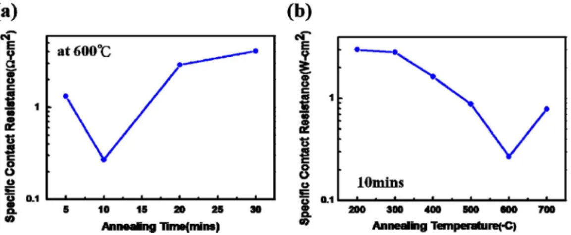
Fig. 2. Specific contact resistance for ITO on p-GaN samples deposited by sputter (a) at fixed annealing temperature of about 600 C (b) with the same annealing time of 10 min.
[19]. The electroluminescence (EL) characteristics of our de-vices were measured by the probe station system at different current density. The output power could be obtained from the optical power-meter through an integrated sphere. Current–light output power (L–I) and current–voltage (I–V) measurements were also performed. In addition, these devices driven by dc current source were analyzed through the charge-coupled de-vice and beam-view instrument. These instruments can show the optical intensity distribution of devices and capture optical intensity distribution of the measured devices. Then, the inten-sity distribution can be digitalized to a 2-D map of inteninten-sity for the current spreading analysis purpose.
III. RESULT ANDDISCUSSION
The annealing temperature of the samples evaporated by e-gun was at 430 C, 1 min by using RTA instrument. The an-nealing temperature has been optimized for ITO A and ITO B. Fig. 2(a) and (b) shows the results of CTLM measurement for ITO deposited by sputter after annealing by RTA with various parameters under N environment. The annealing temperature in Fig. 2(a) was fixed at 600 C and the annealing time used in Fig. 2(b) was 10 min. An optimized temperature and annealing time can be found out at 600 C 10 min under environment. Therefore, we used these annealing parameters for ITO C and D samples in the following experiment.
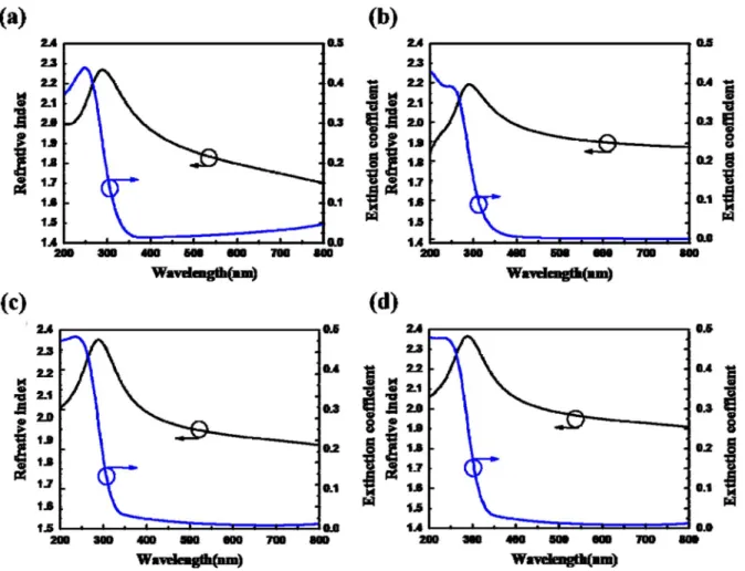
To estimate the material absorption characteristics of ITO film, we measured the refractive index and extinction coeffi-cient from the n&k analyzer. The wavelength dependence of re-fractive index and extinction coefficient for different ITO struc-tures are shown from Fig. 3(a)–(d). The refractive index of GaN-based LEDs with 430 nm is about 2.0. From these figures, the extinction coefficient has a maximum in ultraviolet region be-cause of the interband transition or atomic oscillation [4]. In the visible region, the extinction coefficient is nearly zero and most of light is transparent to most wavelength band. However, the value of absorption in transparent region gradually increases again as wavelength approaches infrared region beyond 800 nm. This increase is due to the vibrational absorption associated with the lattice vibration. The long wavelength absorption can be attributed to the vibrational oscillation in the Lorentz model,
which leads to some loss at this range (especially between vis-ible and IR). The oscillation can come from the bonding be-tween the atoms in the ITO (close to IR range) or from the elec-tronic oscillation in the states (close to visible range). The n&k values in Fig. 3(a) and (b) have larger differences and this could be due to their different grain spacing between larger particles. In Fig. 3(c), the extinction coefficient by sputter is lower than that by e-gun due to the different deposition technology. We be-lieve the lower deposition temperature in the sputter system can help to reduce thermal surface destruction with lower deposi-tion temperature compared to e-gun technology. This feature can provide much better optical characteristics than e-gun tech-nology. The AFM images are shown in Fig. 4. From the AFM results, the surface roughness was measured to be 5.2, 6.6, 0.8, and 0.4 nm with respect to ITO A, ITO B, ITO C, and ITO D, respectively. It shows the surface roughness of ITO C and D is better than ITO A and B. The thin ITO which was deposited by sputter had flatter surface than those deposited by e-gun.
Table II shows the other characteristics of ITO such as sheet resistance, resistivity, and specific contact resistance. The tivity is calculated form the sheet resistance. The sheet resis-tance of ITO A is the lowest compared with 30 nm ITO contact layers due to large thickness. Both optical and electrical proper-ties can be affected by the thickness of ITO [20], and from pre-vious results [20], a thickness between 50 and 100 nm should be best for the external quantum efficiency. However, in our case, due to the requirement of optical loss reduction, we picked 30 nm of ITO as our final choice, and its conductivity is still in the acceptable range. This resistance is associated with lateral cur-rent spreading through the material and it generally decreases as thin film thickness increases. The decreasing of film resistivity could be due to either the increasing carrier concentration and/or Hall mobility in ITO films [21]. However, the specific contact resistance of 30 nm ITO is slightly lower than ITO A. This result reveals the specific contact resistance is not determined by thin film thickness but annealing conditions [22]. Especially, ITO B has the largest sheet resistance and resistivity. We suppose that it could be as a result of its lager vacant space between ITO par-ticles. The results show the deposition quality of e-gun evapo-ration still needs to be improved when deposition thickness is thinner.
Fig. 3. Refractive index and extinction coefficient curves of (a) ITO A, (b) ITO B, (c) ITO C, and (d) ITO D, respectively.
Fig. 4. AFM images of (a) ITO A, (b) ITO B, (c) ITO C, and (d) ITO D, respectively.
Then, these four different ITO structure were applied on RCLEDs and the samples are named RCLED A, RCLED B, RCLED C, and RCLED D, respectively. The performance of
L–I curves and I–V curves was measured by the probe station
and the results are shown in Fig. 5(a) and (b). From these figures, because the surplus nonrecombination carriers become thermalized in the MQW region, the devices would be damaged
TABLE II
ELECTRICALCHARACTERISTICS OFDIFFERENTITO STRUCTURES
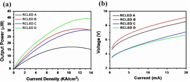
and reduced the recombination efficiency due to higher junc-tion temperature when the output power reaches a maximum value and gradually decay. In Fig. 5(a), the rollover current density of RCLED A, RCLED B, RCLEDC, and RCLED D are 10.5, 12.5, 13.6, and 13.9 KA/cm , respectively. These values exhibits that the effect of heat dissipation of ITO deposited by sputter is better than that by e-gun and the performance of the devices with the RCLED A structure is the worst one. This might be caused by the heat which cannot be easily dissipated from the thick ITO film. Fig. 5(b) shows the I–V curve in each RCLED devices. The turn-ON voltage of RCLED D is about 3 V which is lowest in these devices. In contrast, the turn-ON
Fig. 5. (a) L–I curves and (b) I–V curves of different ITO layers on RCLEDs.
Fig. 6. Device of (a) 20 (b) 25, and (c) 30 m aperture under same current operation.
voltage of RCLED A and RCLED B are higher than RCLED C and RCLED D. This indicates that the interface between the ITO deposited by e-gun and p-GaN is poor and might hinder the electrical conductivity. Next, we measured 50 devices with current aperture diameter of 25 m for every deposition condition with 2-D beam intensity profiler (BeamView), and average the intensity over the radius direction. The standard de-viation is calculated to be 0.1623 times of the average intensity. There are different aperture sizes of devices made in the same sample. As shown in Fig. 6, the beamview images for device of aperture size 20, 25, and 30 m show similar result under 10 mA operation. The size of the aperture would not affect the characteristics of ITO in the range of interest. The normalized results in Fig. 7 demonstrate the different current spreading (and thus the LED output light intensity) between cases: while the sample A shows best normalized light output, the sample D is also comparable in terms of intensity uniformity. The insets in Fig. 7 show the intensity distribution of RCLED D under 10 mA current injection. In the other two cases, condition B is ac-ceptable, but with further degradation in the light intensity, and C is not acceptable because the obvious lack of current lateral spreading. We believe the current-crowding phenomenon and poor conductivity of RCLED C is caused by ion bombardment during the ITO deposition. When the ITO film is deposited on the sample, the p-GaN surface would be slightly damaged. On the other hand, the RCLED D shows uniform current spreading because of the predeposited 10 nm amorphous ITO film whose process is mild and can protect the p-GaN surface. From these data, we can conclude that the new design of ITO D structure
Fig. 7. Integrated intensity distribution from center to edge of the aperture cor-responds to RCLEDs. The inset shows the intensity distribution image of the activated device.
can deliver a good turn-ON voltage plus comparable current spreading to the much thicker and conventional ITO (sample A).
IV. CONCLUSION
To summary, we fabricated and measured four different ITO structures deposited by e-gun and sputter on RCLEDs. By means of CTLM measurement, we can identify the sputter process condition for lower specific contact resistance between p-GaN and ITO. Furthermore, we found that ITO thin films with thickness of 30 nm had slightly lower specific contact resistance compared with samples of 210 nm ITO. In EL mea-surement, RCLED C and RCLED D show better performance in electric characteristics. In addition, the RCLED device using 10 nm amorphous plus 20 nm crystalline ITO especially has the highest output power (39 W) compared with the conventional RCLED A (15 W). The 2-D light intensity map reveals that the current spreading through the active region was more uniform and concentrated in the amorphous/crystalline ITO structure design. From these results, we believe this hybrid deposition
[2] S. Nakamura, M. Senoh, S.-I. Nagahama, N. Iwasa, T. Yamada, T. Matsushita, Y. Sugimoto, and H. Kiyoku, “Room-temperature con-tinuous-wave operation of InGaN multi-quantum-well structure laser diodes,” Appl. Phys. Lett., vol. 69, pp. 4056–4058, 1996.
[3] S. C. Wang, T. C. Lu, C. C. Kao, J. T. Chu, G. S. Huang, H. C. Kuo, S. W. Chen, T. T. Kao, J. R. Chen, and L. F. Lin, “Optically pumped GaN-based vertical cavity surface emitting lasers: Technology and charac-teristics,” Jpn. J. Appl. Phys., vol. 46, pp. 5397–5407, 2007. [4] J. K. Sheu, Y. K. Su, G. C. Chi, P. L. Koh, M. J. Jou, C. M. Chang, C.
C. Liu, and W. C. Hung, “High-transparency Ni/Au ohmic contact to -type GaN,” Appl. Phys. Lett., vol. 74, pp. 2340–2342, 1999. [5] J. W. Bae, H. J. Kim, J. S. Kim, N. E. Lee, and G. Y. Yeom, “Effects
of oxygen ion beam plasma conditions on the properties of indium tin oxide thin films,” Vacuum, vol. 56, pp. 77–81, 2000.
[6] Y. Yao, C. Jin, Z. Dong, Z. Sun, and S. M. Huang, “Improvement in performance of GaN-based light-emitting diodes with indium tin oxide based transparent ohmic contacts,” Display, vol. 28, p. 129, 2007. [7] T. Margalith, O. Buchinsky, D. A. Cohen, A. C. Abare, M. Hansen, S.
P. DenBaars, and L. A. Coldren, “Indium tin oxide contacts to gal-lium nitride optoelectronic devices,” Appl. Phys. Lett., vol. 74, pp. 3930–3932, 1999.
[8] D. W. Kim, Y. J. Sung, J. W. Park, and G. Y. Yeom, “A study of trans-parent indium tin oxide (ITO) contact to p-GaN,” Thin Solid Film, vol. 87, pp. 398–399, 2001.
[9] P. Yu, C. H. Chang, C. H. Chiu, C. S. Yang, J. C. Yu, H. C. Kuo, S. H. Hsu, and Y. C. Chang, “Efficiency enhancement of GaAs photovoltaics employing indium-tin-oxide nano-columns,” Adv. Mater., vol. 21, pp. 1618–1621, 2009.
[10] P. Yu, C. H. Chang, M. S. Su, M. H. Hsu, and K. H. Wei, “Embedded indium-tin-oxide nano-electrodes for efficiency and lifetime enhance-ment of polymer-based solar cells,” Appl. Phys. Lett., vol. 96, pp. 153307-1–153307-3, 2010.
[11] S. H. Su, C. C. Hou, M. Yokoyama, R. S. Shieh, and S. M. Chen, “Tem-perature effect on the optoelectronic properties of GaN-based light-emitting diodes with ITO p-contacts,” J. Electrochem. Soc., vol. 154, pp. 155–158, 2007.
[12] C. Y. Hsu, W. H. Lan, and Y. C. S. Wu, “Thermal annealing effect of indium tin oxide contact to GaN light-emitting diodes,” Jpn. J. Appl.
Phys., vol. 44, pp. 7424–7426, 2005.
[13] M. A. Tsai, P. Yu, C. L. Chao, C. H. Chiu, H. C. Kuo, S. H. Lin, J. J. Huang, T. C. Lu, and S. C. Wang, “Efficiency enhancement and beam shaping of GaN-InGaN vertical-injection light-emitting diodes via high-aspect-ratio nanorod arrays,” IEEE Photon. Technol. Lett., vol. 21, no. 4, pp. 257–259, Feb. 2009.
[14] R. B. H. Tahar, T. Ban, Y. Ohya, and Y. Takahashi, “Tin doped in-dium oxide thin films: Electrical properties,” J. Appl. Phys., vol. 83, pp. 2631–2645, 1998.
[15] T. C. Lu, C. C. Kuo, H. C. Kuo, G. S. Huang, and S. C. Wang, “CW lasing of current injection blue GaN-based vertical cavity surface emit-ting laser,” Appl. Phys. Lett., vol. 92, pp. 141102-1–141102-3, 2008. [16] G. Vanko, T. Lalinsky, Z. Mozolova, J. Liday, P. Vogrincic, A. Vincze,
F. Uherek, S. Hascik, and I. Kostic, “Nb-Ti/Al/Ni/Au based ohmic con-tacts to AlGaN/GaN,” Vacuum, vol. 82, pp. 193–196, 2008. [17] X. S. Yin, W. Tang, X. L. Weng, and L. J. Deng, “Surface morphology
modelling for the resistivity analysis of low temperature sputtered in-dium tin oxide thin films on polymer substrates,” J. Phys. D: Appl.
Phys., vol. 42, pp. 225304-1–225304-8, 2009.
diodes,” J. Electrochem. Soc., vol. 10, pp. 270–272, 2007.
Tzeng-Tsong Wu received the B.S. degree in electrical engineering in 2007 and the M.S. degree in optoelectronic sciences in 2009, both from the National Taiwan Ocean University, Keelung, Taiwan. He is currently working toward the Ph.D. degree in the Department of Photonics, Institute of Electro-Optical Engineering, National Chiao Tung University (NCTU), Hsinchu, Taiwan.
He joined the Semiconductor Laser Technology Laboratory, NCTU in 2009, where he was involved in research on III–V semiconductor materials for semi-conductor lasers under the instruction of Prof. T.-C. Lu and Prof. S.-C. Wang. His recent research interests include GaN-based vertical cavity surface emitting laser, resonance cavity light-emitting diodes, and photonic crystal surface emit-ting laser.
Chien-Chung Lin (S’93–M’02), was born in Taipei, Taiwan, in 1970. He received the B.S. degree in electrical engineering from the National Taiwan University, Taipei, Taiwan, in 1993, and the M.S. and Ph.D. degrees in elec-trical engineering from Stanford University, Stanford, CA, in 1997 and 2002, respectively.
His thesis research was focused on design, modeling, and fabrication of mi-cromachined tunable optoelectronic devices. Since 2009, he has been with Na-tional Chiao-Tung University (NCTU), Tainan, Taiwan, where he is currently an Assistant Professor. The major research efforts in his group are in design and fabrication of semiconductor optoelectronic devices, including LEDs, solar cells, and lasers. Before joining NCTU, he worked for different start-ups in the U.S. In 2002, he joined E2O Communications, Inc., Calabasas, CA, as a Senior Optoelectronic Engineer. His main research interests then were in optically and electrically pumped long-wavelength vertical cavity surface-emitting lasers. In 2004, he joined Santur Corporation, Fremont, CA, where he initially was a member of Technical Staff then became Manager of Laser Chip Engineering later. He had worked on various projects such as monolithic multiwavelength distributed feedback (DFB) laser arrays for data and telecommunications ap-plications, yield and reliability analysis of DFB Laser arrays, etc. He has more than 30 journal and conference publications.
Dr. Lin is a member of IEEE Photonic Society and Electron Devices Society.
Yun-Lin Wu was born in Penghu, Taiwan, on September 5, 1987. He received the B.S. degree in physics from the National Sun Yat-Sen University (NSYSU), Kaohsiung, Taiwan, in 2009. He is currently working toward the M.S. degree at the Institute of Electro-Optical Engineering, National Chiao Tung University, Hsinchu, Taiwan.
His research interests include the simulation, process and characteristics of GaN-based vertical cavity surface emitting laser under the instruction of Prof. T.-C. Lu and Prof. S.-C. Wang.
Chien-Kang Chen was born in Taitung, Taiwan, on January 17, 1985. He re-ceived the M.S. and B.S. degrees from the Department of Material Science and Engineering and the Display Institute, National Chiao Tung University, Hsinchu, Taiwan, in 2007 and 2009, respectively.
He is currently a Senior R&D Engineer in AU Optronics Corporation, Science Park, Hsinchu.
Tien-Chang Lu (M’07) received the B.S. degree in electrical engineering from the National Taiwan University, Taipei, Taiwan, in 1995, the M.S. degree in electrical engineering from the University of Southern California, Los Angeles, in 1998, and the Ph.D. degree in electrical engineering and computer science from the National Chiao Tung University, Hsinchu, Taiwan, in 2004.
He was with the Union Optronics Corporation as a Manager of Epitaxy De-partment in 2004. Since August 2005, he has been with the National Chiao Tung University as a Faculty Member in the Department of Photonics. In 2007 summer, he visited Stanford University for semiconductor microcavity research. He is the author and coauthor of more than 100 internal journal papers. His re-search interests include the design, epitaxial growth, process, and characteri-zation of optoelectronic devices, such as vertical-cavity surface-emitting lasers, photonic crystal lasers, microcavity, wafer-fused flip-chip LEDs, solar cells, etc. He has been involved in the metal–organic chemical vapor deposition epitaxial technique as well as the process development associated with various material systems including InGaAlAs, InGaAsP, AlGaAs, InGaAlP, and InGaAlN. He is also interested in the structure design and simulations for optoelectronic devices using computer-aided software.
Prof. Lu is a recipient of The Exploration Research Award of Pan Wen Yuan Foundation 2007 and Chinese Excellent Young Electronic Engineer Award 2008.
Hao-Chung Kuo (S’98–M’99–SM’06) received the B.S. degree in physics from National Taiwan University, Taipei, Taiwan, the M.S. degree in electrical and computer engineering from Rutgers University, New Brunswick, NJ, in 1995, and the Ph.D. degree from the Department of Electrical and Computer Engineering, University of Illinois at Urbana Champaign, Champaign, in 1999. He has an extensive professional career both in research and industrial re-search institutions that includes: Rere-search Consultant in Lucent Technologies, Bell Laboratories (1993–1995); and a member of Technical Staff in Fiber-Op-tics Division at Agilent Technologies (1999–2001) and LuxNet Corporation (2001–2002). Hong Kong ASTRI (2004). Since October 2002, he has been with the National Chiao Tung University (NCTU) as a Faculty Member of the Insti-tute of Electro-Optical Engineering. He is currently the Chairman, Department of Photonics, Institute of Electro-Optical Engineering, NCTU. He is the author and coauthor of more than 200 SCI journal papers, 200 conference papers, and 8 granted and 14 pending patents. His current research interests include semicon-ductor lasers, vertical cavity surface-emitting lasers, blue and UV LED lasers, quantum-confined optoelectronic structures, optoelectronic materials, and solar cell.
Dr. Kuo is the Associate Editor of the JOURNAL OFLIGHTWAVETECHNOLOGY
and IEEE JOURNAL OFSELECTEDTOPICS INQUANTUMELECTRONICSSPECIAL
ISSUESOLIDSTATELIGHTING. He received Ta-You Wu Young Scholar Award
from National Science Council and Young Photonics Researcher Award in 2007.
Shing-Chung Wang (M’79–SM’03–LM’07) received the B.S. degree in elec-trical engineering from the National Taiwan University, Taipei, Taiwan, the M.S. degree in electrical engineering from the National Tohoku University, Sendai, Japan, and the Ph.D. degree in electrical engineering from the Stanford Univer-sity, Stanford, CA, in 1971.
He has an extensive professional career both in academic and industrial re-search institutions, which includes as follows: member of the faculty at the National Chiao Tung University, Hsinchu, Taiwan (from 1965 to 1967), search Associate with Stanford University (from 1971 to 1974), Senior Re-search Scientist with Xerox Corporation (from 1974 to 1985), and Consulting Scientist with Lockheed-Martin Palo Alto Research Laboratories (from 1985 to 1995). Since 1995, he has been a member of the faculty at the Institute of Electro-Optical Engineering, National Chiao Tung University. He is the au-thor or coauau-thor of more than 160 publications. His current research interests include semiconductor lasers, vertical-cavity surface-emitting lasers, blue and UV lasers, quantum-confined optoelectronic structures, optoelectronic mate-rials, diode-pumped lasers, and semiconductor-laser applications.
Dr. Wang is a Fellow of the Optical Society of America and the recipient of the Outstanding Scholar Award from the Foundation for the Advancement of Outstanding Scholarship.