國
立
交
通
大
學
電子工程學系 電子研究所
碩 士 論 文
以準分子雷射退火製作控制晶界位置之雙閘極
複晶矽薄膜電晶體之研究
Study on the Polycrystalline Silicon Thin-Film Transistors with
Location-Controlled Grain Boundary and Double Gate Structure
Using Excimer Laser Annealing
研 究 生:韋凱方
Kai-Fang Wei
指導教授:鄭晃忠 博士
Dr. Huang-Chung Cheng
以準分子雷射退火製作控制晶界位置之雙閘極
複晶矽薄膜電晶體之研究
Study on the Polycrystalline Silicon Thin-Film Transistors with
Location-Controlled Grain Boundary and Double Gate Structure
Using Excimer Laser Annealing
研 究 生:韋凱方 Student : Kai-Fang Wei
指導教授:鄭晃忠 博士 Advisor : Dr. Huang-Chung Cheng
國立交通大學
電子工程學系 電子研究所碩士班
碩士論文
A Thesis
Submitted to Department of Electronics Engineering
& Institute of Electronics
College of Electrical and Computer Engineering
National Chiao-Tung University
In Partial Fulfillment of the Requirements
For the Degree of Master
In
Electronics Engineering
July, 2007
Hsinchu, Taiwan, Republic of China
以準分子雷射退火製作控制晶界位置之雙閘極
複晶矽薄膜電晶體之研究
研究生:韋凱方 指導教授:鄭晃忠 博士
國立交通大學
電子工程學系 電子研究所碩士班
摘要
近年來,複晶矽薄膜電晶體成為顯示技術的關鍵元件,除了可以應用在系統 面板(System on a Panel, SOP)上,於三維積體電路的實現具備相當大的應用潛 力。雖然透過準分子雷射可有效的提升複晶矽薄膜電晶體複晶矽層的結晶性,但 此方法仍有些許缺點,如隨機的晶界分佈、較窄的製程窗口等等。在這篇論文裡, 我們將提出一種易於控制的結晶方式,並利用該結晶方式配合雙閘極結構來增進 複晶矽薄膜電晶體的特性。在第一個部分,我們稱為梯台式通道結晶法(Elevated Channel Method)之側向 結晶方式將被用於製作控制晶界位置之複晶矽薄膜通道並加以探討,我們將介紹
此種單晶界複晶矽薄膜電晶體成長機制。因為底閘極結構梯台邊緣區域提供了較 厚非晶矽層,而在準分子雷射退火時得以扮演晶種的角色。當雷射能量密度控制 使得較薄的元件通道區域全融,且接近角落較厚的區域半融,如此一來,由通道 兩邊側向成長的晶粒沿著相對的方向往通道中間成長,進而在通道的中心只形成 單一晶界,因而得到大型的晶粒以提升元件的效能。各種各樣的分析方法也將用 來探討晶界控制之複晶矽薄膜層,由掃描式電子顯微鏡,穿透式電子顯微鏡的分 析中可知,我們觀察到大約 0.6μm長的人為控制晶粒。 我們也利用該結晶方式,製作出雙閘極低溫複晶矽薄膜電晶體,並對其電特 性加以研究。在沒有任何氫化的處理之下,其N型元件之等效載子移動率更超過 1000 cm2/V-s,而P型元件則超過 340 cm2/V-s。我們觀察到元件的均勻性也被提 升,在量測二十個元件之下,載子移動率的標準差小於 50 cm2/V-s,臨界電壓的 標準差小於 0.16 V,次臨界擺幅之標準差則小於 0.04 V/decade。而透過雙閘極 之結構,我們也觀察到較為陡峭之次臨界擺幅以及較小的汲極誘導能障下降 (DIBL)。此外,相較於傳統結晶方式之上閘極薄膜電晶體,我們也獲得八倍以上 之驅動電流。 儘管雙閘極結構之複晶矽薄膜電晶體表現出良好的電特性,然而在量測中發 現部分元件之漏電流的問題卻相當嚴重。我們認為漏電流來自於上下兩個閘極在 微影製程造成的不對稱,導致一些隨著梯台式通道結晶法形成的小晶粒在強閘極 逆偏壓時被空乏區所覆蓋,導致當汲極端施加強電場時,一些缺陷中被捕捉的電 子釋放出來而形成漏電流,因此為了解決此問題,我們提出了低汲極摻雜(Lightly Doped Drain, LDD)之雙閘極薄膜電晶體結構,以降低汲極端之電場,將漏電流抑 制下來以提升電流開關比。然而低汲極摻雜也導致轉導衰退與驅動電流減小,因 此我們亦引入了上閘極內縮之結構,以避開小晶粒的方式,在不影響轉導與驅動 電流等電性情況下,達到抑制漏電流之效果。
Study on the Polycrystalline Silicon Thin-Film Transistors
with Location-Controlled Grain Boundary and Double Gate
Structure Using Excimer Laser Annealing
Student: Kai-Fang Wei Advisor: Dr. Huang-Chung Cheng
Department of Electronics Engineering & Institute of Electronics
National Chiao Tung University
ABSTRACT
In recent years, polycrystalline silicon (poly-Si) thin-film transistors (TFTs) were the key devices in flat-panel displays , System on a panel (SOP), and three dimensional integrated circuits (3D-ICs) applications. Although conventional top-gate poly-Si TFTs by excimer laser crystallization was an effective technology to improve the crystallinity of polycrystalline silicon thin films, there were still some drawbacks such as random grain boundaries, narrow process window, etc. In this thesis, we introduced so called elevated channel method to control the grain growth and the location of grain boundary. With the aid of this method and double gate structure, the high performance double gate poly-Si TFTs had been fabricated to obtain single grain boundary in the channel region.
transistors fabricated by excimer laser annealing were investigated. The mechanisms of elevated channel thin films were studied. A thick amorphous silicon region was formed in the both sides of elevated channel on the bottom gate which served as the seeds for the lateral grain growth during excimer laser irradiation. As the laser energy density was controlled to completely melt the thin region in the channel and partially melt the thick region near the corner, the lateral grain growth starting from the sides of elevated channel could progress along the direction toward the center of channel region. There was only one longitudinal grain boundary in the center of the channel. Thus, a large-grain polycrystalline silicon thin film which would lead to improved device performance was obtained. Various analyses were also performed to investigate the elevated channel thin films. From the analyses of scanning electron microscope (SEM), transmission electron microscope (TEM), large longitudinal grains artificially grown were observed to be about 0.6 μm.
Electrical characteristics of single grain-boundary double-gate TFTs were also studied. High-performance SGB-DG-TFTs with equivalent field-effect mobility exceeding 1000 cm2/V-s for n-channel TFTs and 340 cm2/V-s for p-channel TFTs have been fabricated without any hydrogenation treatment. The uniformity was also improved by this method. If twenty SGB-DG-TFTs devices were taken into discussion, the standard deviation of equivalent field-effect mobility was smaller than 50 cm2/V-s and the standard deviation of Vth was smaller than 0.16 V, while that of subthreshold swing was smaller than 40 mV/decade. By means of double gate structure, we obtained steeper subthreshold swing and superior drain-induced- barrier-lowering (DIBL). Furthermore, SGB-DG-TFTs provided 8 times higher driving current than conventional TFTs.
depletion region to the small grain accompanied with the elevated channel structure. During off-state operation, high drain bias voltage causing strong lateral electric field would release the trap charges and lead to the leakage current. Therefore, we proposed two methods for the purpose of the alleviation of leakage current, lightly doped drain (LDD) structure and shrunk gate engineering. For the LDD, the on/off current ratio was increased while the driving current was sacrificed. Therefore, we developed the shrunk gate engineering to achieve the goal of the suppression of leakage current without any sacrifice of transconductance and driving current.
誌 謝
感謝我的論文指導教授鄭晃忠博士,自從大學時代就跟著老師做專題,三年 半來,老師的身教言教,包括研究上的熱心指導以及謙恭溫和的處世態度,讓我 獲益良多。 感謝這幾年帶著我成長兩位學長們。感謝柏廷學長從專題生時代開始對我耐 心的教導,也謝謝你包容我的懶散;感謝春乾學長,半路出家讓你帶的很辛苦, 你毫無怨言的接納跟細心的從基本的機台操作跟製程經驗教起,讓我得以順利邁 向畢業之路。 感謝實驗室的全平學長、國瑞學長、志良學長、國暥學長、高照學長、瑞霖 學長、大傳學長、逸哲學長在知識上的傳承;感謝實驗室同學祐圻、俠威、君翰、 佩琪,兩年來有你們相伴,再沮喪的心情都能夠振作;感謝國科會計畫合作的彥 佑與為鈞,跟你們一起在乾哥的羽翼下長大感覺很好;感謝序恆、仕煒、偉凱、 政欽、建穎學弟與育瑛學妹的生活上的相伴;感謝Class 10 裡面相逢的朋友,因 為有你們讓我熬夜到頭昏腦脹都還是能撐下去;感謝NDL 眾家小姐的鼎力相助 讓我實驗能順利完成;謝謝中華映管的產學合作計畫讓我有學習的機會。 感謝我的父母家人。感謝爸媽從小的教育養成,更謝謝你們從上大學以來給 我極大的空間與信任,讓我自由發展。 無論如何,還是一句謝謝!對於任何曾經關心過我、幫助過我的人。Contents
Abstract (in Chinese)……….i
Abstract (in English)………iii
Acknowledgements (in Chinese)………..………...vi
Contents………...vii
Table Lists………. x
Figure Captions………xii
============================================================= Chapter 1 Introduction……….………...1
1.1 Overview of Low-Temperature Polycrystalline Silicon Thin-Film Transistors (LTPS TFTs)……….………1
1.2 Overview of Crystallization of Amorphous Silicon Thin Films………..2
1.2.1 Solid Phase Crystallization of Amorphous Silicon Thin Films………..2
1.2.2 Metal Induced Crystallization of Amorphous Silicon Thin Films………….3
1.2.3 Laser Irradiation Crystallization of Amorphous Silicon Thin Films………..4
1.3 Motivation………....5
1.3.1 Fabrication of Polycrystalline Silicon Thin Films with Single Grain Boundary………..5
1.3.2 Polycrystalline Silicon TFTs with Double Gate Structure by Elevated Channel Process………...6
1.3.3 Suppression of Leakage Current with Lightly Doped Drain Structure…..…7
1.4 Thesis Organization………..8
Chapter 2 Fabrication of Location-Controlled Single Grain Boundary (SGB) and Double Gate (DG) Polycrystalline Silicon (Poly-Si) Thin-Film
Transistors (TFTs) by Elevated Channel Methods Using Excimer Laser Annealing (ELA)………...9 2.1 Introduction………..9 2.1.1 Introduction to Elevated Channel Methods………...9 2.1.2 Introduction to Single Grain Boundary and Double Gate Polycrystalline
Silicon Thin-Film Transistors Fabricated by Elevated Channel Method….12 2.2 Material Analyses of Single Grain Boundary Polycrystalline Silicon Thin Films
Fabricated by Elevated Channel Methods………. 13 2.2.1 Process Flow of Material Analyses of SGB Poly-Si Thin Film Fabricated
by Elevated Channel Method ………....13 2.2.2 Material Analysis of SGB Poly-Si Thin Film Fabricated by Elevated
Channel Method………...14 2.2.2.1 Scanning Electron Microscope (SEM) Analysis………14 2.2.2.2 Transmission Electron Microscope (TEM) Analysis…………...16 2.3 Fabrication and Electrical Characteristics Analyses of Single Grain Boundary
(SGB) and Double Gate (DG) Polycrystalline Silicon (Poly-Si) Thin-Film
Transistors (TFT) Fabricated by Elevated Channel Method……….17 2.3.1 Process Flow of SGB-DG-TFTs by Elevated Channel Method…………17 2.3.2 Electrical Characteristics of SGB-DG-TFTs by Elevated Channel
Method………...18 2.3.2.1 Electrical Characteristics of SGB-DG-TFTs………..18 2.3.2.2 Uniformity Investigation on SGB-DG-TFTs ………21 2.3.2.3 Dependence of Effective Field Effect Mobility on Applied Laser
Energy Density………..22 2.3.2.4 Activation Energy for Carrier from Source to Drain……….23
Chapter 3 Investigation of the Characteristics of Single Grain Boundary
Low-Temperature Polycrystalline Silicon Thin-Film Transistors with
Double Gate Structure………26
3.1 Introduction………26
3.2 Comparisons of Electrical Characteristics between Top Gate, Bottom Gate and Double Gate TFTs Fabricated by Elevated Channel Method ………27
3.1.1 Process Flow of Top Gate, Bottom Gate and Double Gate TFTs ………….27
3.1.2 Electrical Characteristics Analysis and Comparison of Single Gate Devices and Double Gate Devices………..29
3.3 Leakage Current Issue and Suppression……….30
3.3.1 Leakage Current Mechanism……….30
3.3.2 Suppression of Leakage Current Using Lightly Doped Drain (LDD) Structure………31
3.2.2.1 Introduction………...31
3.2.2.2 Process Flow of DGTFTs with LDD……….32
3.2.2.3 Electrical Characteristics Analysis of DGTFTs with LDD………...33
3.3.3 Suppression of Leakage Current Using Shrunk Gate Engineering………...33
3.2.3.1 Introduction………...33
3.2.3.2 Process Flow of DGTFTs Using Shrunk Gate Engineering ……….34
3.2.3.3 Electrical Characteristics Analysis of DGTFTs Using Shrunk Gate Engineering………...35
3.4 Summary………....36
Chapter 4 Conclusions………..…………37
References………...89
Table Lists
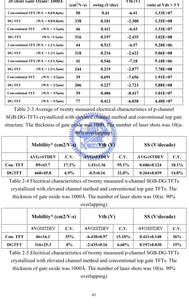
Table 2-1 Average of twenty measured electrical characteristics of n-channel SGB-DG-TFTs crystallized with elevated channel method and conventional top gate structure. The thickness of gate oxide was 1000Å. The number of laser shots was 10(ie. 90% overlapping).
Table 2-2 Average of twenty measured electrical characteristics of n-channel SGB-DG-TFTs crystallized with elevated channel method and conventional top gate structure. The thickness of gate oxide was 1000Å. The number of laser shots was 20(ie. 95% overlapping).
Table 2-3 Average of twenty measured electrical characteristics of p-channel SGB-DG-TFTs crystallized with elevated channel method and conventional top gate structure. The thickness of gate oxide was 1000. The number of laser shots was 10(ie. 90% overlapping).
Table 2-4 Electrical characteristics of twenty measured n-channel SGB-DG-TFTs crystallized with elevated channel method and conventional top gate TFTs. The thickness of gate oxide was 1000Å. The number of laser shots was 10(ie. 90% overlapping)
Table 2-5 Electrical characteristics of twenty measured p-channel SGB-DG-TFTs crystallized with elevated channel method and conventional top gate TFTs. The thickness of gate oxide was 1000Å. The number of laser shots was 10(ie. 90% overlapping)
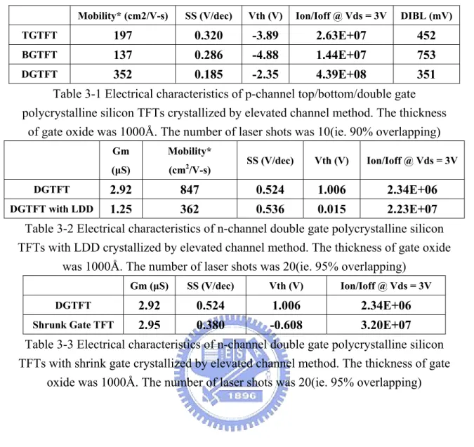
Table 3-1 Electrical characteristics of p-channel top/bottom/double gate poly- crystalline silicon TFTs crystallized by elevated channel method. The thickness of gate oxide was 1000Å. The number of laser shots was 10(ie. 90% overlapping)
Table 3-2 Electrical characteristics of n-channel double gate polycrystalline silicon TFTs with LDD crystallized by elevated channel method. The thickness of gate oxide was 1000Å. The number of laser shots was 20(ie. 95% overlapping)
Table 3-3 Electrical characteristics of n-channel double gate polycrystalline silicon TFTs with shrink gate crystallized by elevated channel method. The thickness of gate oxide was 1000Å. The number of laser shots was 20(ie. 95% overlapping)
Figure Captions
Chapter 2
Fig. 2-1 (a) The schematic illustration of the low energy regime corresponding to energy densities that partially melting the a-Si thin film
Fig. 2-1 (b) The schematic illustration of the high energy regime corresponding to energy densities that completely melting the a-Si thin film
Fig. 2-1(c) The schematic illustration of the super lateral growth regime corresponding to energy densities that nearly completely melting the a-Si thin film
Fig. 2-2 SEM graph of poly-Si by conventional ELA process in SLG regime
Fig. 2-3 Process flow of preparing samples for material characteristics by elevated channel method
Fig. 2-4 The schematic illustration of the excimer laser system.
Fig. 2-5 SEM graphs of excimer laser crystallized polycrystalline silicon by elevated channel method. The channel length was varied from 1μm to 1.5 μm. The bottom poly gate thickness was 1000Å and the gate oxide thickness was 500Å. The laser energy density was 510 mJ/cm2
Fig. 2-6 SEM graphs of excimer laser crystallized polycrystalline silicon by elevated channel method. The channel length was 1.2 μm. The poly gate thickness was 1000Å and the gate oxide thickness was 500Å. The laser energy density was (a) 470 (b) 490 (c) 510 mJ/cm2.
Fig. 2-7 SEM graphs of excimer laser crystallized polycrystalline silicon by elevated channel method. The channel length was (a)1 (b)0.8 (c)0.7 μm. The poly gate thickness was 1000Å and the gate oxide thickness was 500Å. The laser energy density was 310 mJ/cm2.
Fig. 2-8 Cross-section TEM graphs of excimer laser crystallized polycrystalline silicon by elevated channel method.
Fig. 2-9 Cross-section TEM graphs of excimer laser crystallized polycrystalline silicon by elevated channel method.
Fig. 2-10 Process flow for fabrication of SGB-DG-TFTs
Fig. 2-11 Transfer characteristic of n-channel double gate polycrystalline silicon TFTs crystallized using elevated channel method with channel length of 0.8 μm, in which the thickness of gate oxide was 1000 Å. The number of laser shots was 10 (ie. 90% overlapping).
Fig. 2-12 Transfer characteristic of n-channel double gate polycrystalline silicon TFTs crystallized using elevated channel method with channel length of 1 μm, in which the thickness of gate oxide was 1000Å. The number of laser shots was 10 (ie. 90% overlapping).
Fig. 2-13 Transfer characteristic of n-channel double gate polycrystalline silicon TFTs crystallized using elevated channel method with channel length of 1.2 μm, in which the thickness of gate oxide was 1000Å. The number of laser shots was 10 (ie. 90% overlapping).
Fig. 2-14 Transfer characteristic of n-channel double gate polycrystalline silicon TFTs crystallized using elevated channel method with channel length of 1.5 μm, in which the thickness of gate oxide was 1000Å. The number of laser shots was 10 (ie. 90% overlapping).
Fig. 2-15 Transfer characteristic of n-channel double gate polycrystalline silicon TFTs crystallized using elevated channel method with channel length of 2 μm, in which the thickness of gate oxide was 1000Å. The number of laser shots was 10 (ie. 90% overlapping).
Fig. 2-16 Transfer characteristic of n-channel double gate polycrystalline silicon TFTs crystallized using elevated channel method with channel length of 5 μm, in which the thickness of gate oxide was 1000Å. The number of laser shots was 10 (ie. 90% overlapping).
Fig. 2-17 Transfer characteristic of n-channel double gate polycrystalline silicon TFTs crystallized using elevated channel method with channel length of 0.8 μm, in which the thickness of gate oxide was 1000Å. The number of laser shots was 20 (ie. 95% overlapping).
Fig. 2-18 Transfer characteristic of n-channel double gate polycrystalline silicon TFTs crystallized using elevated channel method with channel length of 1 μm, in which the thickness of gate oxide was 1000Å. The number of laser shots was 20 (ie. 95% overlapping).
Fig. 2-19 Transfer characteristic of n-channel double gate polycrystalline silicon TFTs crystallized using elevated channel method with channel length of 1.2 μm, in which the thickness of gate oxide was 1000Å. The number of laser shots was 20 (ie. 95% overlapping).
Fig. 2-20 Transfer characteristic of n-channel double gate polycrystalline silicon TFTs crystallized using elevated channel method with channel length of 1.5 μm, in which the thickness of gate oxide was 1000Å. The number of laser shots was 20 (ie. 95% overlapping).
Fig. 2-21 Transfer characteristic of n-channel double gate polycrystalline silicon TFTs crystallized using elevated channel method with channel length of 2 μm, in which the thickness of gate oxide was 1000Å. The number of laser shots was 20 (ie. 95% overlapping).
Fig. 2-22 Transfer characteristic of n-channel double gate polycrystalline silicon TFTs crystallized using elevated channel method with channel length of 5 μm, in which the thickness of gate oxide was 1000Å. The number of laser shots was 20 (ie. 95% overlapping).
Fig. 2-23 Transfer characteristic of p-channel double gate polycrystalline silicon TFTs crystallized using elevated channel method with channel length of 0.8 μm, in which the thickness of gate oxide was 1000Å. The number of laser shots was 10 (ie. 90% overlapping).
Fig. 2-24 Transfer characteristic of p-channel double gate polycrystalline silicon TFTs crystallized using elevated channel method with channel length of 1 μm, in which the thickness of gate oxide was 1000Å. The number of laser shots was 10 (ie. 90% overlapping).
Fig. 2-25 Transfer characteristic of p-channel double gate polycrystalline silicon TFTs crystallized using elevated channel method with channel length of 1.2 μm, in which the thickness of gate oxide was 1000Å. The number of laser shots was 10 (ie. 90% overlapping).
Fig. 2-26 Transfer characteristic of p-channel double gate polycrystalline silicon TFTs crystallized using elevated channel method with channel length of 1.5 μm, in which the thickness of gate oxide was 1000Å. The number of laser shots was 10 (ie. 90% overlapping).
Fig. 2-27 Transfer characteristic of p-channel double gate polycrystalline silicon TFTs crystallized using elevated channel method with channel length of 2 μm, in which the thickness of gate oxide was 1000Å. The number of laser shots was 10 (ie. 90% overlapping).
Fig. 2-28 Transfer characteristic of p-channel double gate polycrystalline silicon TFTs crystallized using elevated channel method with channel length of 5 μm, in which the thickness of gate oxide was 1000Å. The number of laser shots was 10 (ie. 90% overlapping).
Fig. 2-29 Output characteristic of n-channel double gate polycrystalline silicon TFTs crystallized using elevated channel method with channel length of 0.8 μm, in which the thickness of gate oxide was 1000Å. The number of laser shots was 10 (ie. 90% overlapping).
Fig. 2-30 Output characteristic of n-channel double gate polycrystalline silicon TFTs crystallized using elevated channel method with channel length of 1 μm, in which the thickness of gate oxide was 1000Å. The number of laser shots was 10 (ie. 90% overlapping).
Fig. 2-31 Output characteristic of n-channel double gate polycrystalline silicon TFTs crystallized using elevated channel method with channel length of 1.2 μm, in which the thickness of gate oxide was 1000Å. The number of laser shots was 10 (ie. 90% overlapping).
Fig. 2-32 Output characteristic of n-channel double gate polycrystalline silicon TFTs crystallized using elevated channel method with channel length of 1.5 μm, in which the thickness of gate oxide was 1000Å. The number of laser shots was 10 (ie. 90% overlapping).
Fig. 2-33 Output characteristic of n-channel double gate polycrystalline silicon TFTs crystallized using elevated channel method with channel length of 2 μm, in which the thickness of gate oxide was 1000Å. The number of laser shots was 10 (ie. 90% overlapping).
Fig. 2-34 Output characteristic of n-channel double gate polycrystalline silicon TFTs crystallized using elevated channel method with channel length of 5 μm, in which the thickness of gate oxide was 1000Å. The number of laser shots was 10 (ie. 90% overlapping).
Fig. 2-35 Output characteristic of n-channel double gate polycrystalline silicon TFTs crystallized using elevated channel method with channel length of 0.8 μm, in which the thickness of gate oxide was 1000Å. The number of laser shots was 20 (ie. 95% overlapping).
Fig. 2-36 Output characteristic of n-channel double gate polycrystalline silicon TFTs crystallized using elevated channel method with channel length of 1 μm, in which the thickness of gate oxide was 1000Å. The number of laser shots was 20 (ie. 95% overlapping).
Fig. 2-37 Output characteristic of n-channel double gate polycrystalline silicon TFTs crystallized using elevated channel method with channel length of 1.2 μm, in which the thickness of gate oxide was 1000Å. The number of laser shots was 20 (ie. 95% overlapping).
Fig. 2-38 Output characteristic of n-channel double gate polycrystalline silicon TFTs crystallized using elevated channel method with channel length of 1.5 μm, in which the thickness of gate oxide was 1000Å. The number of laser shots was 20 (ie. 95% overlapping).
Fig. 2-39 Output characteristic of n-channel double gate polycrystalline silicon TFTs crystallized using elevated channel method with channel length of 2 μm, in which the thickness of gate oxide was 1000Å. The number of laser shots was 20 (ie. 95% overlapping).
Fig. 2-40 Output characteristic of n-channel double gate polycrystalline silicon TFTs crystallized using elevated channel method with channel length of 5 μm, in which the thickness of gate oxide was 1000Å. The number of laser shots was 20 (ie. 95% overlapping).
Fig. 2-41 Output characteristic of p-channel double gate polycrystalline silicon TFTs crystallized using elevated channel method with channel length of 0.8 μm, in which the thickness of gate oxide was 1000Å. The number of laser shots was 10 (ie. 90% overlapping).
Fig. 2-42 Output characteristic of p-channel double gate polycrystalline silicon TFTs crystallized using elevated channel method with channel length of 1 μm, in which the thickness of gate oxide was 1000Å. The number of laser shots was 10 (ie. 90% overlapping).
Fig. 2-43 Output characteristic of p-channel double gate polycrystalline silicon TFTs crystallized using elevated channel method with channel length of 1.2 μm, in which the thickness of gate oxide was 1000Å. The number of laser shots was 10 (ie. 90% overlapping).
Fig. 2-44 Output characteristic of p-channel double gate polycrystalline silicon TFTs crystallized using elevated channel method with channel length of 1.5 μm, in which the thickness of gate oxide was 1000Å. The number of laser shots was 10 (ie. 90% overlapping).
Fig. 2-45 Output characteristic of p-channel double gate polycrystalline silicon TFTs crystallized using elevated channel method with channel length of 2 μm, in which the thickness of gate oxide was 1000Å. The number of laser shots was 10 (ie. 90% overlapping).
Fig. 2-46 Output characteristic of p-channel double gate polycrystalline silicon TFTs crystallized using elevated channel method with channel length of 5 μm, in which the thickness of gate oxide was 1000Å. The number of laser shots was 10 (ie. 90% overlapping).
Fig. 2-47 Alleviated kink effect by n-channel SGB-DG-TFTs rather than conventional TFTs. The channel length was 0.8 μm, in which the thickness of gate oxide was 1000Å. The number of laser shots was 10 (ie. 90% overlapping).
Fig. 2-48 Statistics and uniformity of equivalent field effect mobility. Twenty n-channel SGB-DG-TFTs crystallized with elevated channel method and conventional top gate TFTs were measured. The thickness of gate oxide was 1000Å. The number of laser shots was 10(ie. 90% overlapping)
Fig. 2-49 Statistics and uniformity of threshold voltage. Twenty n-channel SGB-DG-TFTs crystallized with elevated channel method and conventional top gate TFTs were measured. The thickness of gate oxide was 1000Å. The number of laser shots was 10(ie. 90% overlapping)
Fig. 2-50 Statistics and uniformity of subthreshold swing. Twenty n-channel SGB-DG-TFTs crystallized with elevated channel method and conventional top gate TFTs were measured. The thickness of gate oxide was 1000Å. The number of laser shots was 10(ie. 90% overlapping)
Fig. 2-51 Statistics and uniformity of equivalent field effect mobility. Twenty p-channel SGB-DG-TFTs crystallized with elevated channel method and conventional top gate TFTs were measured. The thickness of gate oxide was 1000Å. The number of laser shots was 10(ie. 90% overlapping)
Fig. 2-52 Statistics and uniformity of threshold voltage. Twenty p-channel SGB-DG-TFTs crystallized with elevated channel method and conventional top gate TFTs were measured. The thickness of gate oxide was 1000Å. The number of laser shots was 10(ie. 90% overlapping)
Fig. 2-53 Statistics and uniformity of subthreshold swing. Twenty p-channel SGB-DG-TFTs crystallized with elevated channel method and conventional top gate TFTs were measured. The thickness of gate oxide was 1000Å. The number of laser shots was 10(ie. 90% overlapping)
Fig. 2-54 The dependence of equivalent field effect mobility on laser energy densities for n-channel SGB-DG-TFTs crystallized with elevated channel method and conventional TFTs. The thickness of gate oxide was 1000Å. The number of laser shots was 10(ie. 90% overlapping).
Fig. 2-55 The dependence of activation energy of drain current on gate bias voltage for n-channel SGB-DG-TFTs crystallized with elevated channel method. The thickness of gate oxide was 1000Å. The number of laser shots was 10(ie. 90% overlapping).
Fig. 2-56 The dependence of activation energy of drain current on gate bias voltage for n-channel DG-TFTs crystallized with solid phase crystallization. The thickness of gate oxide was 1000Å.
Chapter 3
Fig. 3-1 Process flows for fabrication of SGB-TG-TFTs Fig. 3-2 Process flows for fabrication of SGB-BG-TFTs
Fig. 3-3 Transfer characteristic of p-channel top/bottom/double gate polycrystalline silicon TFTs crystallized using elevated channel method with channel length of 1 μm, in which the thickness of gate oxide was 1000 Å. The number of laser shots was 10 (ie. 90% overlapping).
Fig. 3-4 Output characteristic of p-channel top/bottom/double gate polycrystalline silicon TFTs crystallized using elevated channel method and conventional TFTs with channel length of 1 μm, in which the thickness of gate oxide was 1000 Å. The number of laser shots was 10 (ie. 90% overlapping).
Fig. 3-5 The leakage current issue of n-channel double gate polycrystalline silicon TFTs crystallized using elevated channel method with channel length of 1 μm, in which the thickness of gate oxide was 1000 Å. The number of laser shots was 20 (ie. 95% overlapping).
Fig. 3-6 TEM observation of double gate polycrystalline silicon TFTs crystallized using elevated channel method, in which the thickness of gate oxide was 1000 Å.
Fig. 3-7 The leakage current issue of n-channel double gate polycrystalline silicon TFTs crystallized using elevated channel method measured from Vg = -15V to Vg= 15V with channel length of 1 μm, in which the thickness of gate oxide was 1000 Å. The number of laser shots was 20 (ie. 95% overlapping). Fig. 3-8 The leakage current issue of n-channel double gate polycrystalline silicon
TFTs crystallized using elevated channel method measured from Vg = -20V to Vg= 20V with channel length of 1 μm, in which the thickness of gate oxide was 1000 Å. The number of laser shots was 20 (ie. 95% overlapping). Fig. 3-9 SEM graphs of excimer laser crystallized polycrystalline silicon by elevated
channel method. The channel length was varied from 1μm to 1.5 μm. The bottom poly gate thickness was 1000Å and the gate oxide thickness was 500Å. The laser energy density was 510 mJ/cm2
Fig. 3-10 Process flows for fabrication of SGB-DG-TFTs with LDD Structure
Fig. 3-11 Transfer characteristic of n-channel double gate polycrystalline silicon LDD TFTs crystallized using elevated channel method with channel length of 1 μm, in which the thickness of gate oxide was 1000 Å. The number of laser shots was 20 (ie. 95% overlapping).
Fig. 3-12 Output characteristic of n-channel double gate polycrystalline silicon LDD TFTs crystallized using elevated channel method with channel length of 1 μm, in which the thickness of gate oxide was 1000 Å. The number of laser shots was 20 (ie. 95% overlapping).
Fig.3-13 Process flows for fabrication of SGB-DG-TFTs with Shrunk Gate Engineering
Fig. 3-14 In-line SEM observation of shrunk gate.
Fig. 3-15 Transfer characteristic of n-channel double gate polycrystalline silicon TFTs crystallized using elevated channel method with shrunk gate, in which the thickness of gate oxide was 1000 Å. The number of laser shots was 20 (ie. 95% overlapping).
Fig. 3-16 Output characteristic of n-channel double gate polycrystalline silicon TFTs crystallized using elevated channel method with shrunk gate, in which the thickness of gate oxide was 1000 Å. The number of laser shots was 20 (ie. 95% overlapping).
Chapter 1
Introduction
1.1 Overview of Low-Temperature Poly-
crystalline Silicon Thin-Film Transistors
(LTPS TFTs)
Thin-film transistors (TFTs) have become crucial devices of modern Active Matrix Liquid Crystal Displays (AMLCDs) and Active Matrix Organic Light Emitting Diodes (AMOLEDs) applications [1.1]-[1.5].
Generally, amorphous silicon (a-Si:H) TFTs are the pixel switching elements in AMLCD industry. Amorphous silicon TFTs exhibit low leakage current because of their high off-state resistivity. In addition, they are compatible with large glass substrate for low process temperature. However, the electrical characteristics of a-Si
TFTs such as carrier mobility (typically below 1 cm2/V-s) are inadequate for
peripheral circuits . That is, additional integrated circuits (ICs) are needed to support the function of gate drivers and source drivers to drive a display panel. This will lead
silicon (LTPS) TFTs possesses superior carrier mobility [1.6], greater device reliability, CMOS process capability [1.7], and low temperature process compatibility. Therefore, LTPS TFTs have been investigated to achieve the goal of integrating peripheral circuit in a single panel, which is known as system on panel (SOP) [1.8]. Furthermore, LTPS TFTS have the potential to fulfill the 3-dimentional integrated circuits [1.9].
1.2 Overview of Crystallization of Amorphous
Silicon Thin Films
The crystallinity of poly-Si thin film has great influence on the performance of poly-Si TFTs. For a poly-Si thin film, the grain boundaries cause a lot of defects, which is so called strained bonds and dangling bonds. These defects act as trap states within the band gap and will degrade the electrical characteristics of poly-Si TFTs, such as carrier mobility, threshold voltage, subthreshold swing, and the leakage current. Moreover, the poly-Si TFTs with many defects may suffer reliability issue. It is generally believed that the defects will be reduced by enlarging the grain size. There are several ways to enlarge the grain size, including solid phase crystallization, metal induced crystallization, and laser irradiation crystallization. These methods could be concluded that the a-Si thin films are recrystallized into poly-Si thin film by additional energy. However, there are some differences between these methods and will be introduced in the following three sections.
1.2.1 Solid Phase Crystallization of Amorphous Silicon Thin
Films
The solid phase crystallization (SPC) method is intuitive, with which method the a-Si thin film can be crystallized by thermal annealing. With a view to compatibility with glass substrate, the a-Si thin film is deposited at 550℃ using silane (SiH4). Then followed the SPC process, and the process temperature is kept at 600℃ in N2 ambient, whereas the process time is about 24 hours [1.10]-[1.11].
The grain size of solid phase crystallized poly-Si thin film is several times larger than that of as-deposited poly-Si thin film. Besides, the surface morphology is much smoother in SPC poly-Si thin film than in as-doped ones. However, the SPC TFTs suffers a lot of intra-granular defects and result in a bad performance. The most important of all is the fact that the annealing time is too long and this will limit the throughput to fabricate poly-Si thin film.
1.2.2 Metal Induced Crystallization of Amorphous Silicon
Thin Films
It has been reported that certain metals can induce the crystallization of a-Si thin film. The basic concept of metal induced crystallization (MIC) is furnace annealing, which is analogous to SPC. Compared to SPC, MIC is able to reduce the annealing temperature (<400℃) and process duration (<5hrs); that is, higher throughput can be obtained.
Several metals have been proposed to be applied to MIC process, such as aluminum (Al), aurum (Au), nickel (Ni), platinum (Pt). Among these metals, Ni is the candidate for mainstream industrial application. Nickel silicide will be formed during process and the crystallization of silicon will start. Owing to the very small mismatch (0.4%) of crystal lattice constant between the <111> orientation faces of nickel
However, MIC suffers high leakage current because of the fact that metal residues cannot be avoided after MIC process. The residues act as metal contamination and offer leakage path under carrier transportation.
1.2.3 Laser Irradiation Crystallization of Amorphous Silicon
Thin Films
The laser irradiation crystallization process may be the most promising for grain growth, for the glass substrate not being damaged during laser process [1.16]-[1.17]. The laser modes can mainly be divided into two types, pulse type and continuous wave laser type. The excimer laser emits in UV light region with short pulse duration (10-30ns) by the laser source of ArF, KrF, or XeCl (output wavelengths 193, 248, and 308nm, respectively) gas. On the other hand, the continuous wave (CW) laser emits in green light by the diode-pumped solid-state (DPSS) laser source of Nd:YVO4 (532nm) [1.18].
The benefit of using excimer laser crystallization (ELC) is the strong optical absorption of a-Si thin film to UV lights. During ELC process, a-Si thin films absorb the light, then melt and recrystallize in a short period of time, forming poly-Si grain (~1μm). For the volume expansion from liquid to solid phase, surface roughness (usually called protrusion) occurs after the ELC process. It has been reported that increasing the laser shots will reduce the protrusion and obtain better crystallinity. The definition of laser shots is the overlaps between each laser shot, i.e., 20 shots correspond to 5% overlap per shot. The poly-Si thin film fabricated by ELC suffers from narrow process window and instability of shot-to-shot laser energy, which lead to non-uniformity issue of grain structure.
better uniformity. The power instability is less than 1%, which is superior to that of excimer laser. The continuous wave characteristic makes it possible for grain to grow in a large longitudinal distance (tens ofμm in average). However, the technology has not been well-development and is still under investigation in modern academic research.
1.3 Motivation
In order to fabricate high performance low-temperature polycrystalline silicon thin-film transistor, we introduce several aspects to improve the electrical characteristics of LTPS TFTs: to reduce defects of poly-Si thin film, to raise the gate control ability, and suppress the leakage current. From the view of reducing defects of poly-Si thin film, we introduced a simple method to fabricate high quality poly-Si thin film, which is so called elevated channel structure. When it comes to raising the gate control ability, we propose the double gate structure. The leakage current issue is investigated and alleviated by lightly doped drain structure.
1.3.1 Fabrication of Polycrystalline Silicon Thin Film with
Single Grain Boundary
Although pulsed excimer laser crystallization (ELC) has been widely applied to recrystallize a-Si, narrow process window and the uniformity of crystallized poly-Si thin film are crucial problems. The excimer laser energy should be kept at a certain threshold value to make sure the a-Si thin film is nearly completely melted, which is so called “super lateral growth” (SLG) region; that is, ELC suffers narrow process window. In addition, the shot-to-shot laser energy of ELC is not stable enough and the
ELC process comes out a non-uniform poly-Si thin film.
For the purpose of the issues mentioned above, many researches have been proposed to solve the problem, such as sequential lateral solidification (SLS), phase-modulated ELC, μ-Czochralski (so called grain filter) method, selectively enlarging laser crystallization (SELAX) technology, etc [1.19]-[1.22]. However, these methods are not compatible with the existing excimer laser annealing system or need complex process flows. Therefore, a simple method to control the direction of grain growth and the location of grain boundary has been developed in this thesis, which is called “Elevated Channel Method”. In this method, we can artificially control the thermal gradient in selective region, which is the elevated region, (actually the channel region) formed by bottom gate structure. The step at the corner of bottom gate region is thicker than elsewhere of the other region. If the laser energy density is controlled to completely melt the thinner region and partially melt the thicker region, a lateral thermal gradient will determine the grain growth from the un-melting solid phase seeds towards the melting liquid phase region. For the whole thesis, the crystallization is based on this structure.
1.3.2 Polycrystalline Silicon TFTs with Double Gate
Structure by Elevated Channel Process
It has been demonstrated that the performance of devices can be enhanced with multi-gate structure. These methods, including double gates, dual gates, tri-gates, Ω -gate, and surrounding gate…etc. [1.23]-[1.26], are concentrated on the extension of the field induced channel in the same area. By means of these methods, we can obtain better gate control ability and higher driving current than that of conventional top gate or bottom gate devices. The short channel effect can be alleviated with the strong gate
control ability if the channel region is fully depleted [1.27].
Among the methods mentioned above, the double gate structure is preferred in this thesis because of the compatibility with the elevated channel process. We use the step of the corner of bottom gate structure to control the grain growth and attain single grain boundary in channel region. Therefore the top gate dielectric and top gate electrode can be deposited in the following process. In the first part of this thesis, the device performance is investigated by the combination of elevated channel process and double gate structure.
1.3.3 Suppression of Leakage Current with Lightly Doped
Drain Structure
Low-temperature polycrystalline silicon thin-film transistors suffer storage charge distortion as pixel switches or noise as circuit application if the leakage current is high. Therefore, the suppression of leakage current has become significant issue. The leakage mechanisms of LTPS TFTS have been investigated a lot and are related to the grain boundaries [1.28]-[1.29]. The trap states arisen from grain boundaries act as leakage path at high gate bias and drain bias. Most researches reveal that the lightly doped drain (LDD) or offset structure can eliminate the leakage current [1.30]. Hence, we introduce LDD structure to suppress the leakage current. In this thesis, the LDD structure is formed followed by the gate spacer and then the heavily doped implant. With LDD structure, the electric field near drain can restrain the leakage current from drain to source. In the second part of this thesis, the double gate TFTs with LDD structure are introduced to investigate the leakage current suppression.
1.4 Thesis Organization
In chapter 1, a brief overview of LTPS TFTs technology was given to explain the crystallization process. The motivations of this thesis were subsequently explained to introduce this thesis.
In chapter 2, experimental processes of elevated channel thin films were introduced. The mechanism of lateral growth of elevated channel thin films was proposed by material analysis. The material properties were analyzed by scanning electron microscope (SEM) and transmission electron microscope (TEM). Then experimental procedures of polycrystalline silicon thin-film transistors with double gate structure were introduced. The electrical characteristics, including the field-effect mobility, the subthreshold swing, the threshold voltage, and the uniformity were investigated.
In chapter 3, the double gate devices were compared with the top gate and bottom gate ones. Then the DGTFTs fabricated by elevated channel process were modified with lightly doped drain (LDD) structure and shrunk gate engineering with a view to suppression of leakage current. The process flows and the leakage current lowering mechanism would be discussed in detail.
Chapter 2
Fabrication of Location-Controlled
Single Grain Boundary (SGB) and
Double Gate (DG) Polycrystalline
Silicon (Poly-Si) Thin-Film Transistors
(TFTs) by Elevated Channel Methods
Using Excimer Laser Annealing (ELA)
2.1 Introduction
2.1.1 Introduction to Elevated Channel Methods
Currently, high current-driving capability, low leakage current, and good uniformity of TFT characteristics are essential for the application of AMLCD, AMOLED, and 3-dimensional ICs [2.1]-[2.6]. Low-temperature polycrystalline silicon (LTPS) technology is the most promising method to fabricate high performance thin-film transistors (TFTs) on glass or plastic substrate [2.7]. In comparison with amorphous silicon (a-Si) TFTs, LTPS TFTs exhibit higher field effect-mobility and better reliability, which lead to higher driving current and better
stress resistance. Therefore, LTPS TFTs acting as pixel switches are allowed in smaller size; that is, higher aperture ratio is obtained. Furthermore, LTPS TFTs are compatible with complementary metal-oxide-semiconductor (CMOS) circuits which results in the alleviation of power consumption [2.8]. Consequently, the scan drivers, the data drivers, and even the processors are allowed to be integrated in a single glass substrate for the next generation of system on panel (SOP) application. As compared to high temperature polycrystalline silicon (HTPS) TFTs, the thermal budget of LTPS TFTs is much lower for the process temperature is below 200℃, which means that LTPS TFTs may open a new field for flexible microelectronics [2.9]. Accordingly, the cost of LTPS TFTs is much lower than that of HTPS TFTs.
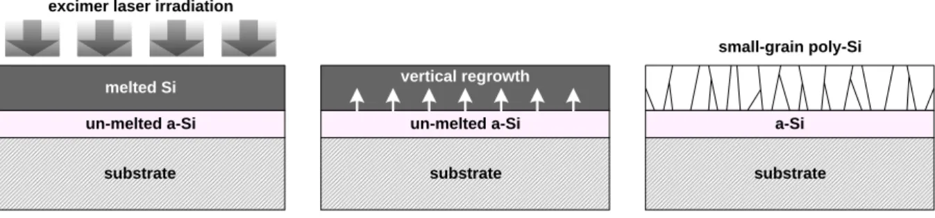
In order to prepare LTPS thin films, several ways have been reported to date, including solid phase crystallization (SPC), metal induced lateral crystallization (MILC), and laser annealing [2.10]-[2.13]. Among these methods, the excimer laser annealing (ELA) may be the most promising one. The excimer laser emits in UV light region with short pulse duration (10-30ns) by the laser source of ArF, KrF, or XeCl (output wavelengths 193, 248, and 308nm, respectively) gas source. The strong optical absorption of UV light and small diffusion length during the laser pulse in silicon imply that high temperature can be produced and cause melting of silicon without significant damage of glass substrate [2.14]. In addition, ELA poly-Si films possess good crystallinity and few intra-grain defects due to the melt-regrowth process. During ELA process, the mechanism of grain growth is quite sensitive to the laser energy density. Fig. 2-1 schematically illustrates the grain growth corresponding to the different laser energy densities. As shown in Fig. 2-1 (a), if the laser energy density is too small to melt the whole a-Si thin film, vertical solidification occurs and the un-melted solid layer remains to be a-Si, while the melted Si layer transform into poly-Si with small grain size [2.15]. Refer to Fig. 2-1 (b), if the laser energy density is
large enough to completely melt the a-Si thin film, homogeneous nucleation occurs for deep supercooling, resulting in small grain size [2.16]. Only when the laser energy density is controlled around a certain threshold value will we obtain large grains whose size are as large as 1μm in diameter, as shown in Fig. 2-1 (c). This is so called
Super Lateral Growth (SLG) regime [2.17], which vividly illustrates the behavior of
melted a-Si to recrystallize from very few un-melted Si residues to each other. For the very few residues as seeds, the lateral growth phenomenon causes large grain size.
However, there are some limits for the ELA process even though we control the laser energy density in SLG regime. First, the seeds of SLG regime appear randomly; that is, the location of grain and grain boundary cannot be controlled and thereafter the large variation of grain size. Fig. 2-2 reveals the non-uniformity of grain size. Second, a lot of process fluctuation factors exist, i.e., the pulse-to-pulse variation of excimer laser energy, the variation of a-Si film thickness, and the narrow process window of ELA process. Therefore, a novel method called Elevated Channel Process is proposed to enhance the uniformity of grain crystallinity and the location of grain and grain boundary. Moreover, with elevated channel process, we obtained much larger process window rather than that of conventional ELA process.
In this chapter, the experimental procedures of elevated channel process would be introduced. We studied the mechanism of lateral growth of elevated channel process by material analysis equipments. The material properties of elevated channel thin films were investigated by scanning electron microscope (SEM) and transmission electron microscope (TEM).
2.1.2 Introduction to Single Grain Boundary and Double
Gate Polycrystalline Silicon Thin-Film Transistors
Fabricated by Elevated Channel Method
High current-driving capability and good uniformity of TFT characteristics over a large area of glass substrate were imperative for devices aiming at AMLCD and AMOLED drivers and matrix [2.18]-[2.22]. Furthermore, they should be produced with low cost and high throughput. It was desired that the growth of high-quality large grain could be controlled in the device channel region from the viewpoint of device performance and uniformity. A novel process for high quality LTPS thin films for producing high-mobility polycrystalline silicon TFTs was described in the section above. We call this novel method, elevated channel method. With this method, single grain boundary (SGB) low-temperature polycrystalline silicon (LTPS) thin-film transistors (TFTs) with double gate (DG) structure were formed. There was only one longitudinal grain boundary in the center of the channel. Besides, it has been reported for integrated circuit (IC) application, a double gate device is expected to obtain ultimate high-performance ideal metal oxide semiconductor field-effect transistors (MOSFETs) [2.23]. Therefore, we can produce silicon-on-insulator-liked (SOI-liked) LTPS TFTs by means of introducing the double gate structure. Furthermore, another advantage of double gate structure is the enhancement of gate controlling ability. With enhanced gate controlling ability, the devices will exhibit high driving current, steeper subthreshold swing, and superior short-channel effect immunity [2.24]-[2.26]. In this section, the detail process flows of SGB-DG- TFTs were introduced. Then the electrical characteristics were measured by electrical parameter analyzer, Agilent 4156. Both the N-type and P-type SGB-DG-TFTs were fabricated in comparison to conventional ones. Moreover, the dependence of laser shots number and electrical
characteristics was investigated. Finally, statistics and uniformity of electrical characteristics exhibited the superiority of SGB-DG-TFTs rather than conventional top gate TFTs.
2.2 Material Analyses of Single Grain Boundary
Polycrystalline Silicon Thin Films
Fabricated by Elevated Channel Methods
2.2.1 Process Flow of Material Analyses of SGB Poly-Si Thin
Films Fabricated by Elevated Channel Method
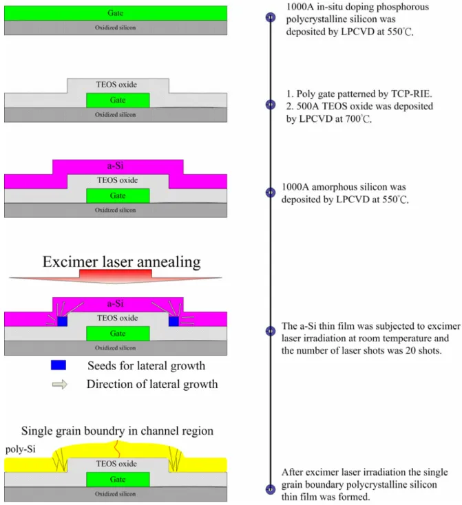
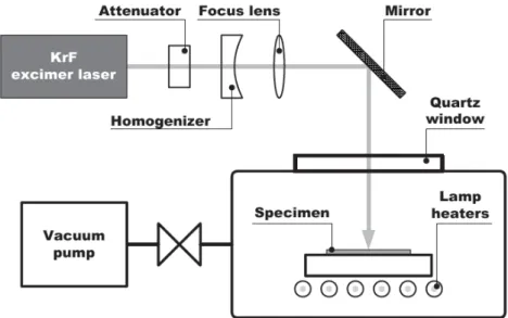
Detailed process flows of prepared samples were shown in Fig. 2-3. At first, in-situ doping phosphorus polycrystalline silicon thin films with thickness of 1000Å were deposited by pyrolysis of pure SiH4 and PH3 by low-pressure chemical vapor deposition (LPCVD) at 550℃ on oxidized silicon substrates with oxide thickness of 1 μm. Then, the doped polycrystalline silicon layer was defined to form polycrystalline silicon gate by transverse coupled plasma reactive ion etch (TCP-RIE). Next, a 500Å TEOS oxide layer was deposited as gate insulator by LPCVD at 700°C. After the deposition of bottom gate insulator, the 1000Å amorphous silicon layer was deposited as the active layer by LPCVD at 550℃ with SiH4 as gas source. The elevated channel was named after the channel region which is elevated for bottom gate structure. Laser crystallization was performed by KrF excimer laser (λ=248nm). The excimer laser system was shown in Fig. 2-4. During the laser irradiation, the samples were located on a substrate in a vacuum chamber pumped down to 10-3Torr
area was 20 (i.e., 95% overlapping) and laser energy density was varied. The grain structure of the crystallized polycrystalline silicon thin film was analyzed using scanning electron microscope (SEM) and transmission electron microscope (TEM). In order to facilitate the SEM observation, all the samples were processed by secco-etch before SEM analysis.
2.2.2 Material Analysis of SGB Poly-Si Thin Film Fabricated
by Elevated Channel Method
2.2.2.1 Scanning Electron Microscope (SEM) Analyses
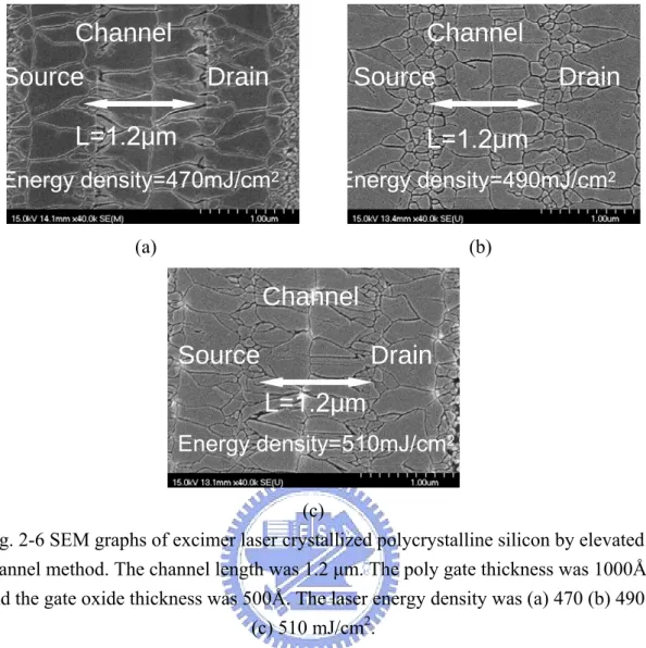
Fig. 2-5 shows SEM graphs of excimer laser crystallized polycrystalline silicon with elevated channel method. The channel length was (a) 1 μm (b) 1.2 μm and (c) 1.5 μm, respectively. The laser energy was 510 mJ/cm2and the poly gate thickness was 1000 Å. The longitudinal grains with 0.6 μm in length were formed in the channel region. It has been reported that lateral thermal gradient could arise as a result of the heat generated at moving solid-melting interface [2.27]. When a proper laser energy density irradiated the silicon thin film containing different thicknesses, the thin region in the channel region was completely melted while the thick region in the corner due to the step structures of bottom gate was only partially melted, leaving behind islands of solid material. As a result, grains would grow laterally towards the complete melting region from the retained solid seeds. The lateral growth would start from the still solid amorphous silicon spacer seeds and stretch toward the completely melted region until the solid-melt interface from opposite direction collided. Due to the in-situ design of thin channel region, the grain boundaries perpendicular to the current flow in the channel region could be reduced. Thus the field-effect mobility of
polycrystalline silicon TFTs could be greatly improved with this crystallization technique. When a longer channel length was adopted for crystallization, the laser fluence would have to be increased high enough to make the longitudinal grains collide with those grown from the other side; otherwise, small grains caused by spontaneous homogeneous nucleation would form in the center of the channel region as Fig.2-5 (c).
With a view to investigating the process window of elevated channel method, we altered the laser energy density irradiated on a-Si thin film. Fig.2-6 shows SEM graphs of poly-Si thin films with different laser energy densities while the channel length was kept at 1.2 μm. As the laser energy density was increased from 470 mJ/cm2 to 510 mJ/cm2, we obtained analogous gate structure in channel region. Therefore, we could conclude that the process window of elevated channel method is much larger than that of conventional excimer laser annealing on whole flat a-Si thin film.
It has been reported that thinner active layer can achieve the “fully depleted” device operation [2.28]. The electrical characteristics of fully depleted devices are much greater than partially depleted ones, such as alleviated kink effect, low threshold voltage, and more ideal subthreshold swing. In our experiment, thinner a-Si thin film (500Å) was also adopted to the elevated channel method. As shown in Fig.2-7, the laser energy density was controlled at 310 mJ/cm2 to completely melt thinner region but partially melted thicker region. However, the a-Si thin film was too thin to keep thermal energy retained in the molten Si channel region and the severe supercooling phenomenon occurred which led to homogenous nucleation. In consequence, small grains were observed in the channel region instead of the lateral grain growth. Therefore, we must use a-Si thin film thickness of 1000 Å to prevent the homogenous
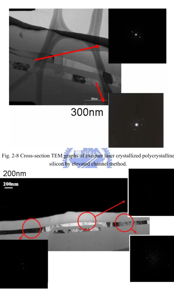
2.2.2.2 Transmission Electron Microscope (TEM) Analysis
Fig. 2-8 shows the cross-section TEM graphs of polycrystalline silicon thin film fabricated by elevated channel method in the channel region. From the Fig. 2-8, it could be found that single grain boundary was controlled artificially at the center of the channel region, and two large grains with very few intra-grain defects were observed. For polycrystalline silicon thin film used as active layer in thin-film transistor, fewer defects were desired. Meanwhile, the cross-section TEM graph of polycrystalline silicon thin film in the corner region the bottom gate shows that the thickness of the corner region became thinner than that in the channel region. From the correlated electron diffraction pattern of polycrystalline silicon thin film, the crystallinity of the polycrystalline silicon was analyzed. It could be found that as the channel region was selected, the diffraction spots become more obvious, which means that the crystallinity was good. When the corner region was selected, the ring was observed, which revealed that the vertical growth in the corner region of the grains exhibit poor crystallinity. But the corner regions would be heavily doped and act as the source/drain region of TFTs. Therefore, the poor crystallinity may not degrade the performance of LTPS-TFTs.
It is notable to keep an eye on the fact that the good crystallinity appeared not only in the channel region but also the regions at both sides away from the corner of bottom gate as shown in Fig. 2-9. This was analogous to the channel region that the thinner a-Si thin films at these sides were completely melted during laser irradiation, resulting in lateral growth of poly-Si grains. That is, we could obtain similar poly-Si grains with fewer defects except the channel. Therefore, elevated channel method has the potential of produce periodic poly-Si grains if the mask is well designed.
2.3 Fabrication and Electrical Characteristics
Analyses of Single Grain Boundary (SGB)
and Double Gate (DG) Polycrystalline
Silicon (Poly-Si) Thin-Film Transistors (TFT)
Fabricated by Elevated Channel Method
2.3.1 Process Flow of SGB-DG-TFTs by Elevated Channel
Method
Detailed process flows of device fabrication were shown in Fig. 2-10. At first, in-situ doping phosphorus polycrystalline silicon thin films with thickness of 1000Å were deposited by pyrolysis of pure SiH4 and PH3 by low-pressure chemical vapor deposition (LPCVD) at 550°C on oxidized silicon substrates with oxide thickness of 1μm. Then, the doped polycrystalline silicon layer was defined to form bottom gate by TCP-RIE. Next, a 1000 Å TEOS oxide layer was deposited as bottom gate insulator by LPCVD at 700°C. After the deposition of bottom gate insulator, the 1000Å amorphous silicon layer was deposition as the active layer by LPCVD at 550
℃ with SiH4 as gas source. Laser crystallization was performed by KrF excimer
laser (λ=248nm). During the laser irradiation, the samples were located on a substrate in a vacuum chamber pumped down to 10-3Torr and the substrate was maintained at room temperature. The number of laser shots per area was 10 or 20 (i.e., 90 or 95% overlapping) and laser energy density was varied. Next, the active region was defined by TCP-RIE. Then, a 1000 Å TEOS oxide layer was deposited as top gate insulator by LPCVD at 700°C followed by in-situ doping phosphorus polycrystalline silicon
layer as top gate electrode. After the deposition of top polycrystalline silicon gate, the contact hole was defined and etched by TCP-RIE and 1:10 dilute Buffer Oxide Etch (BOE) solvent to interconnect top gate and bottom gate electrode. Next, a
phosphorus/BF2 ion implantation with a dosage of 5×1015 cm-2 and energy of
40keV/70keV was performed to form source and drain regions. A 5500Å TEOS oxide layer was then deposited as passivation layer by LPCVD at 700℃ and the implanted dopants were activated by thermal annealing in furnace at 600°C for 9 hours. Then, contact hole opening by TEL5000-RIE and and metallization with Aluminum were carried out. Finally, Aluminum sintering was carried out at 400 ℃ to reduce the series resistance. No hydrogenation plasma treatment was performed during the device fabrication process. For comparison, conventional top-gate ELC polycrystalline silicon TFTs were also fabricated.
2.3.2 Electrical Characteristics of SGB-DG-TFTs by
Elevated Channel Method
2.3.2.1 Electrical Characteristics of SGB-DG-TFTs
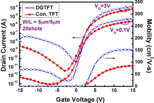
It has been demonstrated that large and longitudinal grains could be formed in the channel region by elevated channel method in section 2.1. The grain structure would have a significant influence on the electrical characteristics of the fabricated TFTs. Fig. 2-11~Fig. 2-16 show the typical transfer characteristics of n-channel SGB-DG-TFTs with channel lengths of 0.8 μm ~5 μm, in which the thickness of gate oxide was 1000Å and the number of laser shots per area was 10(i.e., 90% overlapping). Fig. 2-17 ~Fig. 2-22 show the typical transfer characteristics of n-channel SGB-DG-TFTs with channel lengths of 0.8 μm ~5 μm, in which the
thickness of gate oxide was 1000Å and the number of laser shots per area was 20(i.e., 95% overlapping). Fig. 2-23 ~Fig. 2-28 show the typical transfer characteristics of p-channel SGB-DG-TFTs with channel lengths of 0.8 μm ~5 μm, in which the thickness of gate oxide was 1000Å and the number of laser shots per area was 10. The laser process conditions were optimized and the conventional top gate TFTs were included for comparison. The threshold voltage was defined as the gate voltage required to achieve a normalized drain current of Id = (W/L)×10-8 A at |Vds| =0.1V. The equivalent field-effect mobility was extracted from the maximum transconductance in the linear region of Id-Vg characteristics at |Vd| = 0.1V (i.e., the formula of μ=gm/[(W/L)VdsCox] ). The on/off current ratio was defined as the ratio of maximum drain current over minimum drain current at |Vd| =3V. Several important electrical characteristics of the TFTs were summarized in Table 2-1, Table 2-2 and Table 2-3 for laser shots and channel type of 10/N-type, 20/N-type and 10/P-type, respectively.
It is notable that the definition of field-effect mobility of double gate TFTs was analogous to HARA et al. [2.29] in this thesis. The definition of field-effect mobility could be approached by two aspects. One was the physical meaning of carrier transport capability of poly-Si layer, which was defined by the following equation:
DS ox m V C L W g ⋅ ⋅ ⎟ ⎠ ⎞ ⎜ ⎝ ⎛ = 2 μ ……….(1),
while the channel width was 2W because of the number of field induced channel was two.
The other definition was corresponding to the carrier transport capability in the occupied area of active region, which was defined by the following equation:
DS ox m V C L W g ⋅ ⋅ ⎟ ⎠ ⎞ ⎜ ⎝ ⎛ = * μ ………(2),
while the channel width was W because of the occupied width of active region was only W.
In this thesis, the latter definition was adopted; the name of “equivalent field-effective mobility” and the symbol of “μ*” was used to avoid the confusion with the first definition.
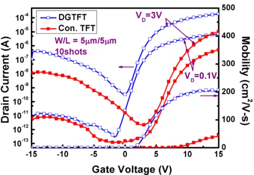
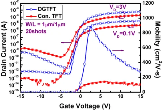
According to Fig. 2-11~Fig. 2-28, the SGB-DG-TFTs exhibit superior electrical characteristics to those of conventional top-gate ones, especially in short channel devices. This could be attributed to the longitudinal grain and single grain boundary in the device channel region. Take the dimension of W = L = 1 μm and laser shots of 10 for example, SGB-DG-TFTs with equivalent field-effect mobility of about 720
cm2/V-s could be achieved by using elevated channel method and double gate
structure while the mobility of the conventional counterpart was about 79 cm2/V-s. Aside from the enhancement of equivalent field-effect mobility, the gate controlling ability of double gate structure could be emphasized by the electrical characteristics of subthreshold swing and drain-induced-barrier-lowering (DIBL, which was defined as the difference of threshold voltage between |Vd| =0.1V and |Vd| =3V). In W = L = 1μm device, we obtained subthreshold swing of SGB-DG-LTPS-TFTs about 0.23V/decade, while that of conventional top gate TFTs was about 0.66V/decade. Similarly, the DIBL of SGB-DG-TFTs was lowered about 200mV rather than that of conventional top gate TFTs. In addition, although the maximum achievable length of lateral grain growth was limited between 0.6 μm as described in the previous section, the electrical characteristics of the TFTs with device dimension up to W = L = 5 μm were still superior to those of conventional ones. This could also ascribed to the long longitudinal grain growth at the channel edge even though many small grains resulted
from spontaneous nucleation exist in the channel center, forming a high series resistance in the middle of channel region as well.
Fig. 2-29 ~Fig. 2-46 display the output characteristics of SGB-DG-TFTs with laser shots and dopant type of 10shots/N-type, 20shots/N-type and 10shots/P-type, respectively. It was demonstrated that SGB-DG-TFTs provide about 8 times higher driving current than conventional ELC polycrystalline silicon TFTs under the same bias condition, especially in short channel devices.
It was reported that the trap center due to grain boundaries enhance kink effect [2.30]-[2.32]. The good crystallinity at the drain edge due to the artificial controlled grain also reduced the kink effect, especially in short channel devices. Fig. 2-47 elaborated more serious kink effect in conventional top gate TFTs than SGB-DG-TFTs.
2.3.2.2 Uniformity Investigation on SGB-DG-TFTs
In the previous section the superior performance of SGB-DG-TFTs than conventional top gate TFTs was highlighted. The uniformity issue of SGB-DG-TFTs would be discussed in this section.
Take the dimension of W = L = 1 and laser shots of for example, Fig. 2-48 ~Fig. 2-50 and Fig. 2-51~Fig. 2-53 show the comparison of equivalent field-effect mobility, threshold voltage, and subthreshold swing for the N-type and P-type devices respectively. Twenty-two TFTs were measured to investigate the device-to-device variation for each dimension, then twenty of which were chosen for the exclusion of unexpected extreme value under statistics. Table 2-4 and Table 2-5 list the average and standard deviation of electrical characteristics. For the accuracy to investigate the precise variation from the mean value, we introduced a parameter from statistics
deviation over mean value in percentage.
Referring to Fig. 2-48~ Fig. 2-53, the values of standard deviation of threshold voltage and subthreshold swing of SGB-DG-TFTs were smaller than those of conventional top gate TFTs, whether N-type devices or P-type devices. However, the value standard deviation of equivalent field-effect mobility seemed to reveal the worse uniformity of SGB-DG-TFTs rather than conventional ones. This illusion might have been reversed with the C.V. When it came to the C.V, we obtained about 7% mobility variation for SGB-DG-TFTs and about 17% mobility variation for conventional top gate devices. Therefore, we concluded that high performance SGB-DG-TFTs with good uniformity could be fabricated easily using elevated channel method with the number of laser shots 10. Therefore, the number of laser shots was reduced and the throughput and the yield could be increased.
2.3.2.3 Dependence of Equivalent Field-Effect Mobility on
Applied Laser Energy Density
Fig. 2-54 displays the dependence of equivalent field effect mobility on laser energy densities for SGB-DG-TFTs and conventional ones. Compared to the conventional top gate TFTs, the SGB-DG-TFTs possessed wide process window by the investigation of mobility. We obtained high equivalent field effect mobility of
SGB-DG-TFTs with laser energy densities varying from 470 to 530 mJ/cm2, while
high mobility of conventional ones was obtained only at 490 mJ/cm2 in contrast. This result corresponded to the material analysis in this chapter that the seed at the corner of step remained partially melted if the laser energy ranged from 470 to 530 mJ/cm2. Besides, the conventional TFTs exhibited good electrical characteristics only at 490mJ/cm2 corresponding to the SLG regime.
![[102-2] WNFA lab4 - A Tiny Wireless Sensor Network](data:image/gif;base64,R0lGODlhAQABAIAAAP///wAAACH5BAEAAAAALAAAAAABAAEAAAICRAEAOw==)