Wavelength Tuning by Bending a
Flexible Photonic Crystal Laser
Kung-Shu Hsu, Tzu-Ting Chiu, Po-Tsung Lee, Member, IEEE, and Min-Hsiung Shih, Member, IEEE, OSA
Abstract—This study demonstrated mechanical wavelength fine-tuning of a flexible photonic crystal (PhC) laser. A triangular PhC structure was fabricated in an InGaAsP layer on top of a poly-dimethylsiloxane substrate. Experiments showed two lasing modes at symmetry points K and M in the first PhC band. The laser struc-ture was bent along the direction and the lasing wavelength was fine-tuned by varying the bending radius. The lasing wave-length shift is attributed to PhC lattice distortion and its tuning behavior corresponds with the simulation results. This ultra-small, wavelength-tunable laser could function as a unique light source for integrated optoelectronic circuits.
Index Terms—Photonic crystals, polymer active devices, semi-conductor lasers.
I. INTRODUCTION
T
WO-DIMENSIONAL photonic crystal (PhC) lasers have attracted attention because of their promising applica-tions as novel light sources in dense chip-scale optical systems [1]. These lasers exhibit excellent optical properties including a small mode volume [2]–[4], high quality factor (Q) [5]–[12], and ultra-low lasing thresholds [13], [14]. Electrically pumped PhC lasers have also been developed recently [15]–[17]. To increase functionality and applications in integrated circuits, on-demand wavelength tuning of PhC lasers is required. Studies have manipulated PhC laser wavelength by varying the envi-ronmental index [18]–[20] or tuning the geometric parameters of the device [21]. Because most PhC lasers are fabricated on hard substrates, it is difficult to control lasing wavelength on-demand by modifying laser geometry once structures are fabricated. Therefore, polymer or organic photonic devices are commonly used because of their flexible applications and low cost. Recent studies have reported on III–V materials-based light emitting diodes [22], [23] and compact lasers [24]–[26] on flexible and stretchable polymer/organic substrates. BecauseManuscript received December 14, 2012; revised March 10, 2013 and April 25, 2013; accepted April 29, 2013. Date of publication May 14, 2013; date of current version May 27, 2013. This study is supported by the National Science Council (NSC) of Taiwan under Grant NSC-99-2112-M-001-033-MY3 and in part by the Grant of the Academic Sinica, Taiwan.
K.-S. Hsu, T.-T. Chiu, and M.-H. Shih are with the Department of Photonics and Institute of Electro-Optical Engineering, National Chiao Tung University, Hsinchu 30010, Taiwan. They are also with the Research Center for Applied Sciences, Academia Sinica, Taipei 115, Taiwan (e-mail: [email protected]. edu.tw).
P.-T. Lee is with the Department of Photonics and Institute of Electro-Optical Engineering, National Chiao Tung University, Hsinchu 30010, Taiwan.
Color versions of one or more of the figures in this paper are available online at http://ieeexplore.ieee.org.
Digital Object Identifier 10.1109/JLT.2013.2262922
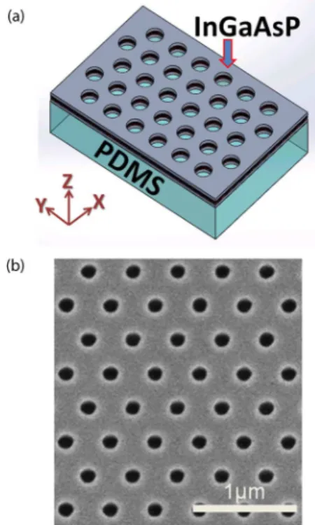
Fig. 1. (a) Illustration of the triangular-lattice PhC band-edge laser on a PDMS substrate. (b) SEM image of the fabrication structure.
the optical properties of compact lasers are sensitive to its ge-ometry, this organic or polymer-semiconductor hybrid platform allows fine-tuning of optical properties for small devices.
In this study, we demonstrate lasing wavelength fine-tuning by manipulating the curvature of flexible PhC lasers. Flexible PhC band-edge lasers are demonstrated by integrating a thin InGaAsP quantum-well (QW) membrane with a flexible poly-dimethylsiloxane (PDMS) substrate, as shown in Fig. 1(a). The low-index PDMS substrate serves as a flexible plat-form to deplat-form the laser structure and supports good optical confinement in a vertical direction. Band-edge lasers exhibit single mode emission characteristics over large areas and high output powers [27]–[30].
II. EXPERIMENT
PhC patterns were fabricated in a 240-nm-thick InGaAsP layer on the InP substrate. The InGaAsP layer consisted of four strained InGaAsP QWs with an emission peak at 1550 nm. A 240-nm-thick silicon-nitride (SiNx) layer and a 300-nm-thick polymethylmethacrylate (PMMA) resist were deposited on the epitaxial wafer for dry etching and electron-beam lithography. Triangular-lattice air holes were defined on PMMA using electron-beam lithography. After the RIE and ICP dry etching
processes, the patterns were transferred to the SiNx layer with a mixture of and gas at 20 and to the QW layer with a mixture of , , and gas at 150 . The QW layer was then bonded to a 500- - PDMS substrate. The structure was formed by removing the InP substrate with a solution of HCl. Fig. 1(b) shows scanning electron microscope (SEM) images of fabricated PhCs. The size of a fabricated photonic crystal structure is approximately .
III. RESULT ANDDISCUSSION
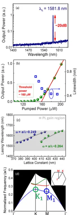
The devices were optically pumped at room temperature using an 850 nm wavelength diode laser at normal incidence with a 1.5% duty cycle and a 30 ns pulse width. The pump beam was focused on the devices using a 100 objective lens. The pumping spot size is fixed to 15 in diameter which covered most area of photonic crystal lattices. Output power from the lasers was measured from the top of the structures with a multi-mode fiber connected to an optical spectrum analyzer. The structure achieved lasing at a low threshold power. Fig. 2(a) shows the lasing spectrum from the PhC band-edge laser with a lattice constant of 395 nm. The lasing wavelength is approx-imately 1581 nm. Fig. 2(b) shows the light-in light-out (L-L) curve for the laser with a threshold power of 160 , which is estimated by the thickness and absorption of the InGaAsP QWs. The measured linewidth (blue dots) at different pumping powers was also plotted in Fig. 2(b) and the quality factor (Q) is approximately 3000 by estimating the ratio of wavelength to linewidth at transparence. To confirm the operating lasing modes of the band-edge laser, structures with different lattice constants were optically-pumped and their lasing wavelengths were recorded. Fig. 2(c) shows the lasing wavelengths from the PhC lattices with different lattice constants. Two groups of these data were identified as operation lasing modes with normalized frequencies of 0.249 and 0.264. These lasing wave-lengths can cover most of the InGaAsP QWs gain region (the gray area). To understand the lasing modes, the corresponding band structure for the TE-like modes was calculated using the three dimensional (3D) plane-wave expansion (PWE) method. Fig. 2(d) shows the photonic crystal band structure below the light-line. Band-edge lasing modes are likely to occur near highly symmetrical band structure points. The flat dispersion curve near the band-edge indicates a low group velocity of light and strong localization. Compared to the simulation and measurements, the 0.249 normalized frequency lasing mode corresponds to the first M band-edge point and the 0.264 mode corresponds to the first K band-edge point. Other band-edge modes were not observed because they fell outside the gain spectrum. The observed lasing modes are all below the light-line of the photonic crystal bandstructure which are guided modes in the photonic crystal slab.
To verify a compact flexible laser can operate on the curved or rough surfaces, we have to characterize the lasing properties by bending the photonic crystal device. The PhC device was bent along the direction of the lattices. Fig. 3(a) shows the illustration of bent PhC lattices with bending radius R along
direction and Fig. 3(b) shows the illustration of and direction of the PhC lattices. Fig. 3(c) shows the
Fig. 2. (a) Lasing spectrum of the triangular-lattice PhC band-edge laser on a PDMS substrate. (b) The L-L curve of the flexible photonic crystal lasers and the linewidth of lasing peak at different pumping powers. (c) The lasing wavelength versus the lattice constant of the band-edge laser and the InGaAsP QW PL gain region. The normalized frequencies of the lasing modes are approximately 0.249 and 0.264. (d) Band structure of the triangular-lattice PhC with a 0.25 r/a ratio.
real devices with the bending. In the experiment, the devices were placed on a bent metal surface at the bending stage, and the bending radius R was controlled by the micrometer. The stage is shown in the Fig. 3(d). The maximal bending curvature reached an approximate bending radius of 20 mm. This is sufficiently large for most applications. At the same pumping conditions and pumping position, the fabricated structure achieved lasing at various bending curvatures.
Fig. 3. (a) Illustration of the bent PhC laser. (b) The propagation directions of the photonic crystal lattices. (c) Bent PhC device. (d) Curved sample on a bent mental surface at bending stage.
Since the PDMS substrate is much thinker than photonic crystal slab and can support the uniform extension. Therefore we can characterize the photonic crystal was photonic lattice expanded uniformly along direction during bending, which is shown in Fig. 4(a). Fig. 4(b) shows the PhC lattices extended percentage varied with the bending curvature. The PhC lattices were extended to 0.15% when the bending radius reached 20 mm. The lasing wavelength bending property was measured several rounds to ensure that mechanical wavelength tuning of PhC band-edge lasers on flexible substrates is repeat-able and relirepeat-able. Fig. 4(c) and 4(d) show lasing wavelengths of the and modes as the bending radius decreased from the flat . The solid lines in the Fig. 4(c) and 4(d) are the calculated wavelengths of the lasing modes from the 3D PWE simulation. The lasing wavelength was red-shift as the bending radius decreased. The Band band-edge modes had different red-shift responses to the bending radius change. In Fig. 4(d), the and modes split from the mode when the laser was bent.
The solid lines in Fig. 4(c) and 4(d) show the simulated wave-length of the band-edge modes by using the 3D PWE method. The resonant frequencies of the and modes decreased with two distinct peak shifts and the mode split into two modes: and . Fig. 4(e) shows the simulated field mode profile corresponding to modes , , and . The lasing oscillation of the band-edge mode exists in three M directions of the triangular lattices [29]. When the lattice was
Fig. 4. (a) Diagram of PhC lattice distortion. (b)The PhC lattices extended percentage varied with the bending curvature. (c) and (d) Comparison between measured lasing frequency (dots) and lattice distortion frequency (lines). (e) Calculated mode profiles of the , , and band-edge modes. (f) The quality factor of the laser with different bending curvatures.
extended in the direction, band-edge mode degen-eracy was broken and split into two modes. The lasing oscilla-tion of the band-edge mode occurs along the bending di-rection and the mode is composed of lasing oscillations in two other directions. By contrast, the band-edge mode did not split significantly when the lattice is extended in the direction. Because the band-edge mode consists of three nonparallel wave vectors which form a closed loop [29], the mode has less impact due to the lattice deformation in the direction. A good agreement is obtained between the simulation and measurement. The small difference between the measurement and simulation results is attributed to an in-accuracy in the PDMS index variation [31]. The wavelength tunability by bending of the , and modes are 16.5
, 9.6 and 28.9 , respectively.
Since the propagation directions of the mode are more par-allel to the direction, and it has the stronger dependence to the lattice extension. Therefore the mode has a higher tun-ability, as expected. To ensure photonic crystal extension during bending, we also fabricated the photonic crystal with lattice ex-tension along direction as the reference devices. The ref-erence devices showed the same tuning behavior to the flexible photonic crystal laser during bending. The results indicate that the flexible PhC laser can serve as a wavelength-tunable light source by mechanically deforming the laser structure. It could also be used as a novel, highly sensitive, ultra-compact optical sensor for local geometry deformation.
Fig. 4(f) shows the quality factor of the flexible PhC laser at different bending radii. The quality factor (Q) decreased only 15% when the laser was bent from flat to 50 mm bending radius, and the threshold of the photonic crystal laser also shows a small increase of 18%. The small variations during the bending indicate it is capable to be a reliable semiconductor laser working on the curved surfaces. We should note that the photonic crystal is embedded inside the low index
PDMS layer which is benefit to optical confinement of the laser. Compare to the suspended membrane type photonic crystal lasers [5]–[9].[10]–[12], this flexible photonic crystal doesn’t have an ultra-high quality factor because of its lower index
con-trast . However the
current photonic crystal laser still has a high Q value of 3000, which is high enough to be a low threshold semiconductor laser. The high-Q photonic crystal structures can be expected with the further studies.
IV. CONCLUSIONS
This study produces a flexible triangular-lattice PhC band-edge laser on a PDMS substrate with a wavelength of approxi-mately 1550 nm and low threshold power. The observed lasing mode occurs about symmetry points K and M of the first PhC band. The bent structure achieves lasing at different bending curvatures and lasing mode red-shifts are observed, which are attributed to lattice distortion and PDMS index variation. From the 3D PWE simulation result, the lattice deformation is domi-nated in wavelength variation when the structure is bent along directions. These observations indicate that this flex-ible PhC laser senses geometry variation instantaneously and
can serve as an ultra-compact, wavelength-tunable light source for photonic integrated circuits.
ACKNOWLEDGMENT
The authors thank the Center for Nano Science and Tech-nology in the National Chiao Tung University for the fabrication facilities.
REFERENCES
[1] O. Painter, R. K. Lee, A. Scherer, A. Yariv, J. D. O’Brien, P. D. Dapkus, and I. Kim, “Two-dimensional photonic band-gap defect mode laser,” Science, vol. 284, p. 1819, 1999.
[2] K. Nozaki and T. Baba, “Laser characteristics with ultimate-small modal volume in photonic crystal slab point-shift nanolasers,” Appl. Phys. Lett., vol. 88, p. 211101, 2006.
[3] H.-S. Ee, K.-Y. Jeong, M.-K. Seo, Y.-H. Lee, and H.-G. Park, “Ultra-small square-lattice zero-cell photonic crystal laser,” Appl. Phys. Lett., vol. 93, p. 011104, 2008.
[4] A. Tandaechanurat, S. Iwamoto, M. Nomura, N. Kumagai, and Y. Arakawa, “Increase of Q-factor in photonic crystal H1-defect nanocav-ities after closing of photonic bandgap with optimal slab thickness,” Opt. Exp., vol. 16, p. 448, 2008.
[5] Y. Akahane, T. Asano, B.-S. Song, and S. Noda, “High-Q photonic nanocavity in a two-dimensional photonic crystal,” Nature, vol. 425, p. 944, 2003.
[6] B.-S. Song, S. Noda, T. Asano, and Y. Akahane, “Ultra-high-Q pho-tonic double-heterostructure nanocavity,” Nature Mater., vol. 4, p. 207, 2005.
[7] E. Kuramochi, M. Notomi, S. Mitsugi, A. Shinya, and T. Tanabe, “Ultrahigh-Q photonic crystal nanocavities realized by the local width modulation of a line defect,” Appl. Phys. Lett., vol. 88, p. 041112, 2006.
[8] M. H. Shih, W. Kuang, A. Mock, M. Bagheri, E. H. Hwang, J. D. O’Brien, and P. D. Dapkus, “High-quality-factor photonic crystal het-erostructure laser,” Appl. Phys. Lett., vol. 89, p. 101104, 2006. [9] Y. Zhang, M. Khan, Y. Huang, J. Ryou, P. Deotare, R. Dupuis, and M.
Lončar, “Photonic crystal nanobeam lasers,” Appl. Phys. Lett., vol. 97, p. 051104, 2010.
[10] B.-H. Ahn, J.-H. Kang, M.-K. Kim, J.-H. Song, B. Min, K.-S. Kim, and Y.-H. Lee, “One-dimensional parabolic-beam photonic crystal laser,” Opt. Exp., vol. 18, p. 5654, 2010.
[11] K. Rivoire, S. Buckley, and J. Vuckovic, “Multiply resonant photonic crystal nanocavities for nonlinear frequency conversion,” Opt. Exp., vol. 19, p. 22198, 2011.
[12] T.-W. Lu, P.-T. Lin, and P.-T. Lee, “Photonic crystal horizontally slotted nanobeam cavity for silicon-based nanolasers,” Opt. Lett., vol. 37, p. 569, 2012.
[13] S. Strauf, K. Hennessy, M. T. Rakher, Y.-S. Choi, A. Badolato, L. C. Andreani, E. L. Hu, P. M. Petroff, and D. Bouwmeester, “Self-tuned quantum dot gain in photonic crystal lasers,” Phys. Rev. Lett., vol. 96, p. 127404, 2006.
[14] M. Nomura, S. Iwamoto, N. Kumagai, and Y. Arakawa, “Ultra-low threshold photonic crystal nanocavity laser,” Phys. E, vol. 40, p. 1800, 2008.
[15] H.-G. Park, S.-H. Kim, M.-K. Seo, Y.-G. Ju, S.-B. Kim, and Y.-H. Lee, “Characteristics of electrically driven two-dimensional photonic crystal lasers,” IEEE J. Quantum Electron., vol. 41, no. 9, p. 1131, Sep. 2005.
[16] B. Ellis, M. A. Mayer, G. Shambat, T. Sarmiento, J. Harris, E. E. Haller, and J. Vučkovic, “Ultralow threshold electrically pumped quantum-dot photonic-crystal nanocavity laser,” Nature Photon., vol. 5, p. 297, 2011.
[17] K. Takeda, T. Sato, A. Shinya, K. Nozaki, H. Taniyama, M. Notomi, K. Hasebe, T. Kakitsuka, and S. Matsuo, “Continuous wave operation of electrically driven wavelength-scale embedded active-region photonic-crystal lasers at room temperature,” in Proc. CLEO 2012, pp. 1–2. [18] M. Lončar, A. Scherer, and Y. M. Qiu, “Photonic crystal laser sources
for chemical detection,” Appl. Phys. Lett., vol. 82, pp. 4648–4650, 2003.
[19] F. B. Arango, M. B. Christiansen, M. Gersborg-Hansen, and A. Kris-tensen, “Optofluidic tuning of photonic crystal band edge lasers,” Appl. Phys. Lett., vol. 91, p. 223503, 2007.
[20] S. Kita, K. Nozaki, and T. Baba, “Refractive index sensing utilizing a cw photonic crystal nanolaser and its array configuration,” Opt. Exp., vol. 16, p. 8174, 2008.
[21] K. Hennessy, A. Badolato, A. Tamboli, P. M. Petroff, and E. Hu, “Tuning photonic crystal nanocavity modes by wet chemical digital etching,” Appl. Phys. Lett., vol. 87, p. 021108, 2005.
[22] S. Park, Y. Xiong, R.-H. Kim, P. Elvikis, M. Meitl, D.-H. Kim, J. Wu, J. Yoon, C.-J. Yu, Z. Liu, Y. Huang, K. Hwang, P. Ferreira, X. Li, K. Choquette, and J. A. Rogers, “Printed assemblies of inorganic light-emitting diodes for deformable and semitransparent displays,” Science, vol. 325, p. 977, 2009.
[23] R.-H. Kim, D.-H. Kim, J. Xiao, B. H. Kim, S. Park, B. Panilaitis, R. Ghaffari, L. Yao, M. Li, Z. Liu, V. Malyarchuk, D. G. Kim, A.-P. Le, R. G. Nuzzo, D. L. Kaplan, F. G. Omenetto, Y. Haung, Z. Kang, and J. A. Rogers, “Waterproof AlInGaP optoelectronics on stretchable substrates with applications in biomedicine and robotics,” Nature Mater., vol. 9, p. 929, 2010.
[24] M. H. Shih, K. S. Hsu, Y. C. Wang, Y. C. Yang, S. K. Tsai, Y. C. Liu, Z. C. Chang, and M. C. Wu, “Flexible compact microdisk lasers on a polydimethylsiloxane (PDMS) substrate,” Opt. Exp., vol. 17, p. 991, 2009.
[25] M. H. Shih, K. S. Hsu, W. Kuang, Y. C. Yang, Y. C. Wang, S. K. Tsai, Y. C. Liu, Z. C. Chang, and M. C. Wu, “Compact optical curvature sensor with a flexible microdisk laser on a polymer substrate,” Opt. Lett., vol. 34, p. 2733, 2009.
[26] S. Riechel, C. Kallinger, U. Lemmer, J. Feldmann, A. Gombert, V. Wittwer, and U. Scherf, “A nearly diffraction limited surface emitting conjugated polymer laser utilizing a two-dimensional photonic band structure,” Appl. Phys. Lett., vol. 77, p. 2310, 2000.
[27] M. Imada, S. Noda, A. Chutinan, T. Tokuda, M. Murata, and G. Sasaki, “Coherent two-dimensional lasing action in surface-emitting laser with triangular-lattice photonic crystal structure,” Appl. Phys. Lett., vol. 75, pp. 316–318, 1999.
[28] S. Noda, M. Yokoyama, M. Imada, A. Chutianan, and M. Mochizuki, “Polarization mode control of two dimensional photonic crystal laser by unit cell structure design,” Science, vol. 293, pp. 1123–1125, 2001. [29] M. Notomi, H. Suzuki, and T. Tamamura, “Directional lasing oscilla-tion of two-dimensional organic photonic crystal lasers at several pho-tonic band gaps,” Appl. Phys. Lett., vol. 78, p. 1325, 2001.
[30] D. Ohnishi, T. Okano, M. Imada, and S. Noda, “Room temperature continuous wave operation of a surface emitting two-dimensional pho-tonic crystal diode laser,” Opt. Exp., vol. 12, pp. 1562–1568, 2004. [31] K. Hoshino and I. Shimoyama, “An elastic thin-film micolens array
with a pneumatic actuator,” in Proc. IEEE Conf. Micro Electro Me-chanical Systems (Institute of Electrical and Electronics Engineers, In-terlaken, Switzerland), 2001, pp. 321–324.
Kung-Shu Hsu was born in Miaoli, Taiwan, R.O.C. He received M.S. degree
from National Chiao Tung University (NCTU), in 2009. He is currently Ph.D. candidate in Institute of Electro-Optical Engineering at the National Chiao Tung University, Hsinchu, Taiwan.
His study is focus on flexible semiconductor laser and flexible photonic de-vices which have high lasing efficiency and high flexibility. He used the com-pact microdisk laser to combine PDMS flexible polymer substrate for his master thesis. His Ph.D. research includes fabrication, simulation, and characterization for flexible photonic devices.
Tzu-Ting Chiu received the M.S. degrees in Department of Photonics from the
National Chiao-Tung University, Hsinchu, Taiwan, in 2011. His research inter-ests include fabrication, simulation, and characterization for flexible photonic devices.
Po-Tsung Lee (M’06) received the B. S. degree from the Department of Physics,
National Taiwan University (NTU), Taipei, Taiwan, in 1997 and the M. S. and Ph.D. degrees from the Department of Electrical Engineering-Electrophysics, University of Southern California (USC), Los Angeles, USA, in 1998 and 2003, respectively. During the Ph.D. study, she was engaged in photonic crystal mi-crocavity lasers. Prof. Lee was the recipient of the University of Southern Cal-ifornia Women in Science and Engineering (WISE) Award in 2000–2001.
In 2003, she joined the Institute of Electro-Optical Engineering, National Chiao Tung University (NCTU), Hsinchu, Taiwan, as an Assistant Professor. In 2007, she became an Associate Professor in the Department of Photonics, NCTU. Her recent research interests are III–V semiconductor photonic crystal active and passive devices and their applications, metallic nanostructures with localized surface plasmon resonances, and silicon-based solar cell technologies. She received the “Excellent Young Electrical Engineer Award” of the Chinese Institute of Electrical Engineering in 2011.
Min-Hsiung Shih received B.S degree in physics from the National Cheng
Kung University, Tainan, Taiwan, in 1995, the M.S. degree in physics from the National Tsing Hua University (NTHU), Taiwan in 1997, and the Ph.D. degree in electrical engineering/electrophysics from the University of Southern Cali-fornia (USC), Los Angeles, USA in 2006.
He is current an Associate Research Fellow in the Research Center for Ap-plied Sciences (RCAS), Academia Sinica and an Adjunct Associate Professor in department of Photonics, National Chiao Tung University (NCTU), Taiwan. His research interests include integrated photonic circuits, photonic crystals, GaN based lasers, surface plasmonics, and cavity quantum electrodynamics. Dr. Shih had authored more than 70 journal and conference publications and is a member of the Institute of Electrical and Electronics Engineers (IEEE) and the Optical Society of America (OSA).